Questions as text
Q1 · Printed circuit board (PCB) manufacture can involve the use of hazardous chemicals 0445/42 May/June 2017
5 Printed circuit board (PCB) manufacture can involve the use of hazardous chemicals. Give two ways of controlling these hazards in a school workshop. 1 … 2 … [2]
2 marks
Mark scheme: 5 Chemical hazards can be controlled by: • Storing in locked cupboards • Clear labelling on containers • Only having small amounts available at one time • Reading COSHH notes or other safety notes • Having precautions nearby when using them 2 mark Allow use of a ventilation system Allow ‘use supervision / technician’ Allow reference to correct disposal
This question in 0445/42 May/June 2017
Q2 · Two input transducers with their circuit symbols 0445/42 May/June 2017
6 Fig. 2 shows two input transducers with their circuit symbols. A B Fig. 2 (a) State the physical property that will change in value in both transducers when they are in use. … [1] (b) Explain why transducer A will react to changing conditions faster than transducer B. … … … [2]
3 marks
Mark scheme: 6(a) Resistance will change 1 6(b) Light can be absorbed and reacted to faster than heat Heat takes longer to be conducted through the body of the thermistor Reference to light [1], Reference to heat [1] 2
This question in 0445/42 May/June 2017
Q3 · A 12-way rotary switch 0445/42 May/June 2017
7 Fig. 3 shows a 12-way rotary switch. common terminal flat Fig. 3 (a) Describe the operation of a 12-way rotary switch. … … … [2] (b) State the purpose of the flat on the spindle of the rotary switch. … [1]
3 marks
Mark scheme: 7(a) In a rotary switch a number of terminals [1] are joined in turn to a common terminal [1] as the switch shaft is rotated 2 7(b) The flat is to allow a control knob to be attached without rotating on the spindle 1 Total: 25
This question in 0445/42 May/June 2017
Q4 · A steel strip in a test rig 0445/42 May/June 2017
8 (a) Fig. 4 shows a steel strip in a test rig. C steel strip load weights Fig. 4 (i) Give the name of electronic component C. … [1] (ii) State the physical property that will change in component C when the load is increased. … [1] (iii) Component C could be attached to either the top or bottom face of the steel strip. State the force being measured according to which face of the steel strip is used. top face … … bottom face … … [2] (iv) Use sketches and notes to show how a non-electronic method could be used to test the amount of movement in the steel strip when a load is applied. [3] (b) Fig. 5 shows packaging for a delicate electronic device. The moulded inner packaging fits inside the assembled outer. When the box is assembled no glue is used. outer packaging - flat corrugated card moulded inner packaging Fig. 5 (i) Give two reasons why the assembled packaging provides protection to the contents when it is being transported. 1 … 2 … [2] (ii) The card used in the construction of the outer packaging is corrugated, a shape that can also be applied to plastic or metal sheet. Use sketches and notes to show what is meant by the term ‘corrugated’. [2] (iii) Fig. 6 shows a frame for a carport. The roof is to be covered using six uncut corrugated plastic sheets 2600 mm × 800 mm. m 2.5 wall 80° 4 m driveway Fig. 6 Draw on Fig. 6 to show two of the corrugated plastic sheets correctly positioned on the roof frame. [2] (c) (i) Fig. 7a and Fig. 7b show two views of a beam used to support a pulley for raising loads on a building site. Fig. 7a Fig. 7b Draw the following methods of reinforcement: • a gusset plate on Fig. 7a • a brace on Fig. 7b [3] (ii) Fig. 7c shows an alternative method of supporting the beam. 800 30° 200N Fig. 7c Draw a scaled force triangle in the space below to calculate the magnitude of the force acting on the chain in Fig. 7c. The diagram has been started for you. 30° Force acting on the chain … N [3] (d) Tall garden plants will often need supporting. Use sketches and notes to show a structure supporting a plant that has reached a height of 1.5 m. Give details of suitable materials for the structure and for any joints used. [4] (e) Explain, using an example, what is meant by torsion in a structure. … … … … [2]
25 marks
Mark scheme: 8(a)(i) Strain gauge 1 8(a)(ii) Very small changes in resistance will be registered by the gauge when it is stretched 1 Allow mark for Resistance without reference to the level of change 8(a)(iii) The steel strip will register tension on the top face and compression on the bottom face 2 Both points must be mentioned in the explanation for 2 marks 8(a)(iv) The non-electronic method must use a dial gauge to register movement when the steel strip is loaded Dial gauge [1] in a suitable position [1] fastening method to the test rig indicated [1] 3 8(b)(i) Reasons for strength of packaging will include: • Folds on long edges, double triple thickness • Locking tabs used with cut outs for edges to fit • Flat sides are supported by strengthened edges • One piece of card used, no extra joints • Folded edges on lids • Inner package is moulded, curves giving strength to the shape • Ribs used on the moulded inner packaging • Absorb shock / impact 2 Allow other valid reasons 1 mark for each valid reason 2 × 1 marks 8(b)(ii) Regular shape / uniform pitch [1] and height [1] of corrugation Accept either with outer sheets or without, corrugations can be square 2 Accept triangular corrugations 8(b)(iii) Corrugations running from wall to edge [1] overlap visible [1] 2 Question Answer Marks Guidance 8(c)(i) Gusset plate principle [1] Brace principle [1] Functional proportions on both methods [1] 3 8(c)(ii) Scaled line to represent 200 N [1] Triangle completed [1] Force in chain taken from drawing – 400 N [1] 3 Allow 1 mark for force calculated rather than using diagram 8(d) Structure stable in three dimensions [1] Height of structure 1.5 m or greater [1] Materials noted [1] Joints described or clearly drawn [1] 4 8(e) Explanation to include the term ’twisting’ or similar term [1] Valid example given [1] 2 Total: 25 R S
This question in 0445/42 May/June 2017
Q5 · Four different types of switch 0445/42 May/June 2017
10 (a) Fig. 12 shows four different types of switch. A C B D … switch … switch … switch … switch Fig. 12 (i) Complete the labels on Fig. 12 to identify the types of switch. [4] (ii) Name the component that is used to operate switch A. … [1] (iii) Fig. 13 shows a DPDT slide switch with information about the contacts. 6 position 1 position 2 5 2 3 terminals 1&2 2&3 4 2 connected 4&5 5&6 1 position connecting wires 1 position Fig. 13 Draw on Fig. 13 to show the connections that will allow the switch to operate as a single pole single throw (SPST) switch. [2] (iv) State the numbers of the two common terminals. … [2] (b) Fig. 14 shows a touch pad sensor circuit used to operate a motor. +6 V Y +12 V touch pads D1 RLA1 R1 X M VR1 TR1 0 V Fig. 14 (i) Give two reasons for using a relay to switch the motor on and off. 1 … … 2 … … [2] (ii) Fig. 15 shows component D1. Fig. 15 Explain why component D1 is included in the circuit. … … … … [2] (iii) To operate the motor the voltage at point X must be at least +0.6 V. Explain how the transistor TR1 will use that voltage to power the relay. … … … … [3] (iv) The power rating of the motor is 100 W. Calculate the maximum current in the motor circuit. Use the formula P = V × I. … … … [2] (v) Choose a suitable relay for the motor circuit from the table below. SPDT 6 A DPDT 6 A DPDT 6 A SPDT 10 A DPDT 16 A 6 V coil 6 V coil 12 V coil 6 V coil 12 V coil … [1] (vi) Give the name of component Y in Fig. 14. … [1] (c) (i) Fig. 16 shows a circuit diagram and the start of a PCB layout for an LED lamp that uses two LEDs in series. view from top of PCB + + – – Fig. 16 Add the following to the PCB layout: • Tracks for the LEDs and resistor • Track for the on/off switch [3]
23 marks
Mark scheme: 10(a)(i) A reed switch, B is a microswitch, C rocker switch, D push switch (PTM or PTB) 1 mark each 4 10(a)(ii) A magnet is used to operate a reed switch 1 10(a)(iii) Connections made to either 1 and 2, 2 and 3, 4 and 5 or 5 and 6. 2 × 1 marks 2 Allow marks if connections go through terminals 1–4, 2–5 etc. No marks for joining all contacts together or for both contacts to one terminal One terminal connected correctly e.g. 1 and 3, 1 mark 10(a)(iv) Common terminals are 2 and 5, 2 × 1 marks 2 10(b)(i) Reasons for a relay could be: • To allow different voltages on motor and control circuit • To allow higher current in motor circuit • To isolate control and motor circuit 2 × 1 marks for valid reasons 2 10(b)(ii) Explanation to include, prevention of back emf, to protect the transistor 2 Both points required for 2 marks 10(b)(iii) Explanation to include: Voltage in base / emitter circuit is used to switch the transistor on [1] The collector / emitter circuit will then start to conduct [1] Current in collector / emitter circuit is depends on the gain of the transistor [1] 3 All three points to be included for 3 marks. Two points – 2 marks One point – 1 mark 10(b)(iv) Current = 100/12 [1] = 8.3A [1]. 2 × 1 marks 2 10(b)(v) Suitable relay is SPDT 10A 6V coil [1] 1 10(b)(vi) Component Y is a fuse [1] 1 co Question Answer Marks Guidance 10(c)(i) 1 mark for each correct 3 Allow different arrangement of tracks if correct and functional 10(c)(ii) Reasons for using a terminal block will include: • Ease of connecting / disconnecting • Less strain on the battery wires, no breaks at soldered joint • Larger wired can be used • No heat involved in changing wires / switch 2 Explanation with two clear points made, 2 marks, allow 2 marks for one well explained point One point made, 1 mark Total: 25 + - [1] [1] [1]
This question in 0445/42 May/June 2017
Q6 · Printed circuit board (PCB) manufacture can involve the use of hazardous chemicals 0445/43 May/June 2017
5 Printed circuit board (PCB) manufacture can involve the use of hazardous chemicals. Give two ways of controlling these hazards in a school workshop. 1 … 2 … [2]
2 marks
Mark scheme: 5 Chemical hazards can be controlled by: • Storing in locked cupboards • Clear labelling on containers • Only having small amounts available at one time • Reading COSHH notes or other safety notes • Having precautions nearby when using them 2 mark Allow use of a ventilation system Allow ‘use supervision / technician’ Allow reference to correct disposal
This question in 0445/43 May/June 2017
Q7 · Two input transducers with their circuit symbols 0445/43 May/June 2017
6 Fig. 2 shows two input transducers with their circuit symbols. A B Fig. 2 (a) State the physical property that will change in value in both transducers when they are in use. … [1] (b) Explain why transducer A will react to changing conditions faster than transducer B. … … … [2]
3 marks
Mark scheme: 6(a) Resistance will change 1 6(b) Light can be absorbed and reacted to faster than heat Heat takes longer to be conducted through the body of the thermistor Reference to light [1], Reference to heat [1] 2
This question in 0445/43 May/June 2017
Q8 · A 12-way rotary switch 0445/43 May/June 2017
7 Fig. 3 shows a 12-way rotary switch. common terminal flat Fig. 3 (a) Describe the operation of a 12-way rotary switch. … … … [2] (b) State the purpose of the flat on the spindle of the rotary switch. … [1]
3 marks
Mark scheme: 7(a) In a rotary switch a number of terminals [1] are joined in turn to a common terminal [1] as the switch shaft is rotated 2 7(b) The flat is to allow a control knob to be attached without rotating on the spindle 1 Total: 25
This question in 0445/43 May/June 2017
Q9 · A steel strip in a test rig 0445/43 May/June 2017
8 (a) Fig. 4 shows a steel strip in a test rig. C steel strip load weights Fig. 4 (i) Give the name of electronic component C. … [1] (ii) State the physical property that will change in component C when the load is increased. … [1] (iii) Component C could be attached to either the top or bottom face of the steel strip. State the force being measured according to which face of the steel strip is used. top face … … bottom face … … [2] (iv) Use sketches and notes to show how a non-electronic method could be used to test the amount of movement in the steel strip when a load is applied. [3] (b) Fig. 5 shows packaging for a delicate electronic device. The moulded inner packaging fits inside the assembled outer. When the box is assembled no glue is used. outer packaging - flat corrugated card moulded inner packaging Fig. 5 (i) Give two reasons why the assembled packaging provides protection to the contents when it is being transported. 1 … 2 … [2] (ii) The card used in the construction of the outer packaging is corrugated, a shape that can also be applied to plastic or metal sheet. Use sketches and notes to show what is meant by the term ‘corrugated’. [2] (iii) Fig. 6 shows a frame for a carport. The roof is to be covered using six uncut corrugated plastic sheets 2600 mm × 800 mm. m 2.5 wall 80° 4 m driveway Fig. 6 Draw on Fig. 6 to show two of the corrugated plastic sheets correctly positioned on the roof frame. [2] (c) (i) Fig. 7a and Fig. 7b show two views of a beam used to support a pulley for raising loads on a building site. Fig. 7a Fig. 7b Draw the following methods of reinforcement: • a gusset plate on Fig. 7a • a brace on Fig. 7b [3] (ii) Fig. 7c shows an alternative method of supporting the beam. 800 30° 200N Fig. 7c Draw a scaled force triangle in the space below to calculate the magnitude of the force acting on the chain in Fig. 7c. The diagram has been started for you. 30° Force acting on the chain … N [3] (d) Tall garden plants will often need supporting. Use sketches and notes to show a structure supporting a plant that has reached a height of 1.5 m. Give details of suitable materials for the structure and for any joints used. [4] (e) Explain, using an example, what is meant by torsion in a structure. … … … … [2]
25 marks
Mark scheme: 8(a)(i) Strain gauge 1 8(a)(ii) Very small changes in resistance will be registered by the gauge when it is stretched 1 Allow mark for Resistance without reference to the level of change 8(a)(iii) The steel strip will register tension on the top face and compression on the bottom face 2 Both points must be mentioned in the explanation for 2 marks 8(a)(iv) The non-electronic method must use a dial gauge to register movement when the steel strip is loaded Dial gauge [1] in a suitable position [1] fastening method to the test rig indicated [1] 3 8(b)(i) Reasons for strength of packaging will include: • Folds on long edges, double triple thickness • Locking tabs used with cut outs for edges to fit • Flat sides are supported by strengthened edges • One piece of card used, no extra joints • Folded edges on lids • Inner package is moulded, curves giving strength to the shape • Ribs used on the moulded inner packaging • Absorb shock / impact 2 Allow other valid reasons 1 mark for each valid reason 2 × 1 marks 8(b)(ii) Regular shape / uniform pitch [1] and height [1] of corrugation Accept either with outer sheets or without, corrugations can be square 2 Accept triangular corrugations 8(b)(iii) Corrugations running from wall to edge [1] overlap visible [1] 2 Question Answer Marks Guidance 8(c)(i) Gusset plate principle [1] Brace principle [1] Functional proportions on both methods [1] 3 8(c)(ii) Scaled line to represent 200 N [1] Triangle completed [1] Force in chain taken from drawing – 400 N [1] 3 Allow 1 mark for force calculated rather than using diagram 8(d) Structure stable in three dimensions [1] Height of structure 1.5 m or greater [1] Materials noted [1] Joints described or clearly drawn [1] 4 8(e) Explanation to include the term ’twisting’ or similar term [1] Valid example given [1] 2 Total: 25 R S
This question in 0445/43 May/June 2017
Q10 · Four different types of switch 0445/43 May/June 2017
10 (a) Fig. 12 shows four different types of switch. A C B D … switch … switch … switch … switch Fig. 12 (i) Complete the labels on Fig. 12 to identify the types of switch. [4] (ii) Name the component that is used to operate switch A. … [1] (iii) Fig. 13 shows a DPDT slide switch with information about the contacts. 6 position 1 position 2 5 2 3 terminals 1&2 2&3 4 2 connected 4&5 5&6 1 position connecting wires 1 position Fig. 13 Draw on Fig. 13 to show the connections that will allow the switch to operate as a single pole single throw (SPST) switch. [2] (iv) State the numbers of the two common terminals. … [2] (b) Fig. 14 shows a touch pad sensor circuit used to operate a motor. +6 V Y +12 V touch pads D1 RLA1 R1 X M VR1 TR1 0 V Fig. 14 (i) Give two reasons for using a relay to switch the motor on and off. 1 … … 2 … … [2] (ii) Fig. 15 shows component D1. Fig. 15 Explain why component D1 is included in the circuit. … … … … [2] (iii) To operate the motor the voltage at point X must be at least +0.6 V. Explain how the transistor TR1 will use that voltage to power the relay. … … … … [3] (iv) The power rating of the motor is 100 W. Calculate the maximum current in the motor circuit. Use the formula P = V × I. … … … [2] (v) Choose a suitable relay for the motor circuit from the table below. SPDT 6 A DPDT 6 A DPDT 6 A SPDT 10 A DPDT 16 A 6 V coil 6 V coil 12 V coil 6 V coil 12 V coil … [1] (vi) Give the name of component Y in Fig. 14. … [1] (c) (i) Fig. 16 shows a circuit diagram and the start of a PCB layout for an LED lamp that uses two LEDs in series. view from top of PCB + + – – Fig. 16 Add the following to the PCB layout: • Tracks for the LEDs and resistor • Track for the on/off switch [3]
23 marks
Mark scheme: 10(a)(i) A reed switch, B is a microswitch, C rocker switch, D push switch (PTM or PTB) 1 mark each 4 10(a)(ii) A magnet is used to operate a reed switch 1 10(a)(iii) Connections made to either 1 and 2, 2 and 3, 4 and 5 or 5 and 6. 2 × 1 marks 2 Allow marks if connections go through terminals 1–4, 2–5 etc. No marks for joining all contacts together or for both contacts to one terminal One terminal connected correctly e.g. 1 and 3, 1 mark 10(a)(iv) Common terminals are 2 and 5, 2 × 1 marks 2 10(b)(i) Reasons for a relay could be: • To allow different voltages on motor and control circuit • To allow higher current in motor circuit • To isolate control and motor circuit 2 × 1 marks for valid reasons 2 10(b)(ii) Explanation to include, prevention of back emf, to protect the transistor 2 Both points required for 2 marks 10(b)(iii) Explanation to include: Voltage in base / emitter circuit is used to switch the transistor on [1] The collector / emitter circuit will then start to conduct [1] Current in collector / emitter circuit is depends on the gain of the transistor [1] 3 All three points to be included for 3 marks. Two points – 2 marks One point – 1 mark 10(b)(iv) Current = 100/12 [1] = 8.3A [1]. 2 × 1 marks 2 10(b)(v) Suitable relay is SPDT 10A 6V coil [1] 1 10(b)(vi) Component Y is a fuse [1] 1 co Question Answer Marks Guidance 10(c)(i) 1 mark for each correct 3 Allow different arrangement of tracks if correct and functional 10(c)(ii) Reasons for using a terminal block will include: • Ease of connecting / disconnecting • Less strain on the battery wires, no breaks at soldered joint • Larger wired can be used • No heat involved in changing wires / switch 2 Explanation with two clear points made, 2 marks, allow 2 marks for one well explained point One point made, 1 mark Total: 25 + - [1] [1] [1]
This question in 0445/43 May/June 2017
Q11 · Three switches and their circuit symbols 0445/41 Oct/Nov 2017
1 (a) Fig. 1 shows three switches and their circuit symbols. A B C Fig. 1 Use the information in Fig. 1 to complete the table below. Contact Type Action arrangement Switch A on / off / on SPDT Switch B push switch SPST Switch C push switch PTM [3] (b) Circle the number of connections that a double pole double throw (DPDT) switch will have. 1 3 4 6 8 [1]
4 marks
Mark scheme: 1(a) 1 mark for each correct. 3 1(b) Circle should be around 6. 1 Type Action Contact arrangement push switch SPST SPDT push switch on / off Switch A Switch B Switch C PTM toggle switch PTB SPST
This question in 0445/41 Oct/Nov 2017
Q12 · An LED, a resistor and an ammeter in a circuit 0445/41 Oct/Nov 2017
2 Fig. 2 shows an LED, a resistor and an ammeter in a circuit. +6 V A 0 V Fig. 2 Complete the circuit to show the ammeter connected to measure the current flow when the LED is lit. [3]
3 marks
Mark scheme: A +6V 0V [1] [1] [1] 2 LED Anode to +6 V, 1 mark Ammeter connected in series (could be above LED or below resistor), 1 mark Resistor connected to 0 V, 1 mark. 3 of connection are possible but LED anode has to be connected to +6V either directly or below ammeter.
This question in 0445/41 Oct/Nov 2017
Q13 · A transistor can be used as an electronic switch 0445/41 Oct/Nov 2017
3 A transistor can be used as an electronic switch. Give two advantages of a transistor switch over a mechanical switch such as a push switch. 1 … 2 … [2]
2 marks
Mark scheme: 3 Advantages of transistor switch could be: • Fast switching • No contact bounce / no moving parts • Low cost • Not manually operated • Low failure rate • Smaller than a mechanical switch 1 mark for each valid advantage 2 Allow other valid advantages. E.g. low current used to switch a higher current.
This question in 0445/41 Oct/Nov 2017
Q14 · A voltmeter ready to be connected to a partly completed circuit 0445/41 Oct/Nov 2017
12 (a) Fig. 13 shows a voltmeter ready to be connected to a partly completed circuit. from power supply V Fig. 13 (i) Complete the connections to the voltmeter. [1] (ii) The reading on the voltmeter is +9.5 V. The resistance of the signal lamp is 60 Ω. Calculate the current in the circuit. Use the formula I = V/R … … [2] (iii) Calculate the power of the signal lamp. Use the formula P = VI … … [2] (b) A printed circuit board (PCB) and an IC holder are shown in Fig. 14. Fig. 14 (i) Give two reasons for tinning the pads on a PCB. 1 … … 2 … … [2] (ii) Describe three stages in fitting and soldering an IC holder into a PCB. 1 … 2 … 3 … [3] (iii) Fig. 15 shows a resistor that has slipped out of position while being soldered into a PCB. correct position Fig. 15 Use sketches and notes to describe how the resistor can be moved to the correct position against the PCB. [3] (c) Fig. 16 show symbols for two, 2 input OR gates. Fig. 16 (i) Connect the 2 input OR gates to make a 3 input OR gate. [1] (ii) Label the 3 inputs. [1] (d) Fig. 17 shows the outputs of a programmable IC (PIC) used to control a simple traffic light sequence on two sets of traffic lights at a road works. Each set of lights has only red and green lights for stop and go. +5 V set B red Sequence of Logic level of outputs out 0 lights on set B green out 1 set A set B out 0 out 1 out 2 out 3 red green 0 1 1 0 set A red out 2 set A green red red out 3 green red red red PIC 0 V Fig. 17 (i) Complete the table to show the logic level of the lights. The first row has been completed for you. [3] (ii) Complete Fig. 18 to show a circuit connected to output 2 that uses an NPN transistor to provide a higher current suitable for a high power LED. +5 V out 0 out 1 out 2 out 3 PIC 0 V Fig. 18 [4]
22 marks
Mark scheme: 12(a)(i) 1 mark for both voltmeter connections correct. 1 12(a)(ii) Current calculation 1 mark for 9.5 / 60 = 0.16 A or 158 mA, 1 mark 2 . V from power supply Question Answer Marks Guidance 12(a)(iii) Power calculation P = 9.5 × 0.158, 1 mark =1.5 W, 1 mark. 2 Allow ecf on value of current 12(b)(i) Reasons for tinning will include: • Prevent oxide formation on the copper track / pads • Make soldering easier / solder adheres better to a tinned surface • Better chance of a successful joint. 2 × 1 marks 2 12(b)(ii) Stages could include: • Putting notch next to pin 1 on board • Aligning all pins with holes • Checking that no pins are folded under the holder • Bending pins on track side to keep IC holder in place • Application of soldering iron to both pin and pad 3 × 1 marks for valid stages 3 12(b)(iii) • Notes and sketches to show board inverted and supported under resistor [1] • Joint heated with soldering iron[1] • Pressure applied to push resistor down[1]. 3 Allow use of desoldering tool rather than soldering iron. 12(c)(i) Output of one gate to an input of the other, 1 mark 1 Other arrangements are possible but all must have an output connected to an input. 12(c)(ii) Labels correct for 3 inputs, 1 mark. 1 [1] input 1 input 2 input 3 Question Answer Marks Guidance 12(d)(i) 1 mark for each correct row, 3 × 1 marks. 3 12(d)(ii) 4 Connections must be all correct for 4 marks. Allow marks for using a relay, 4 marks from • Current limiting resistor • Relay coil connected correctly • diode connected in reverse bias • Transistor connections correct • LED connected correctly through relay contacts. set 1 set 2 red green green red red red red red 0 out 0 out 1 out 2 out 3 1 1 0 Sequence of lights on Logic level of outputs 1 1 1 1 1 1 0 0 0 0 0 0 out 0 out 1 out 2 out 3 PIC +5V 0V [1] [1] [1] [1] out 0 out 1 out 2 out 3 PIC +5V 0V out 0 out 1 out 2 out 3 PIC +5V 0V [1] [1] [1] [1] Question Answer Marks Guidance 12(d)(iii) Explanation could include: • Ease of changing delays • Ease of changing sequence during development • Higher number of usable inputs and outputs • Sequence can easily be changed after manufacture • Low cost of PIC compared to discrete components • Circuit will be less complicated / fewer components • Additional features can be built in. 3 × 1 marks for each point used. Allow 2 marks for one point well explained. 3 Allow other valid points in explanation
This question in 0445/41 Oct/Nov 2017
Q15 · Three switches and their circuit symbols 0445/42 Oct/Nov 2017
1 (a) Fig. 1 shows three switches and their circuit symbols. A B C Fig. 1 Use the information in Fig. 1 to complete the table below. Contact Type Action arrangement Switch A on / off / on SPDT Switch B push switch SPST Switch C push switch PTM [3] (b) Circle the number of connections that a double pole double throw (DPDT) switch will have. 1 3 4 6 8 [1]
4 marks
Mark scheme: 1(a) 1 mark for each correct. 3 1(b) Circle should be around 6. 1 Type Action Contact arrangement push switch SPST SPDT push switch on / off Switch A Switch B Switch C PTM toggle switch PTB SPST
This question in 0445/42 Oct/Nov 2017
Q16 · An LED, a resistor and an ammeter in a circuit 0445/42 Oct/Nov 2017
2 Fig. 2 shows an LED, a resistor and an ammeter in a circuit. +6 V A 0 V Fig. 2 Complete the circuit to show the ammeter connected to measure the current flow when the LED is lit. [3]
3 marks
Mark scheme: A +6V 0V [1] [1] [1] 2 LED Anode to +6 V, 1 mark Ammeter connected in series (could be above LED or below resistor), 1 mark Resistor connected to 0 V, 1 mark. 3 of connection are possible but LED anode has to be connected to +6V either directly or below ammeter.
This question in 0445/42 Oct/Nov 2017
Q17 · A transistor can be used as an electronic switch 0445/42 Oct/Nov 2017
3 A transistor can be used as an electronic switch. Give two advantages of a transistor switch over a mechanical switch such as a push switch. 1 … 2 … [2]
2 marks
Mark scheme: 3 Advantages of transistor switch could be: • Fast switching • No contact bounce / no moving parts • Low cost • Not manually operated • Low failure rate • Smaller than a mechanical switch 1 mark for each valid advantage 2 Allow other valid advantages. E.g. low current used to switch a higher current.
This question in 0445/42 Oct/Nov 2017
Q18 · A voltmeter ready to be connected to a partly completed circuit 0445/42 Oct/Nov 2017
12 (a) Fig. 13 shows a voltmeter ready to be connected to a partly completed circuit. from power supply V Fig. 13 (i) Complete the connections to the voltmeter. [1] (ii) The reading on the voltmeter is +9.5 V. The resistance of the signal lamp is 60 Ω. Calculate the current in the circuit. Use the formula I = V/R … … [2] (iii) Calculate the power of the signal lamp. Use the formula P = VI … … [2] (b) A printed circuit board (PCB) and an IC holder are shown in Fig. 14. Fig. 14 (i) Give two reasons for tinning the pads on a PCB. 1 … … 2 … … [2] (ii) Describe three stages in fitting and soldering an IC holder into a PCB. 1 … 2 … 3 … [3] (iii) Fig. 15 shows a resistor that has slipped out of position while being soldered into a PCB. correct position Fig. 15 Use sketches and notes to describe how the resistor can be moved to the correct position against the PCB. [3] (c) Fig. 16 show symbols for two, 2 input OR gates. Fig. 16 (i) Connect the 2 input OR gates to make a 3 input OR gate. [1] (ii) Label the 3 inputs. [1] (d) Fig. 17 shows the outputs of a programmable IC (PIC) used to control a simple traffic light sequence on two sets of traffic lights at a road works. Each set of lights has only red and green lights for stop and go. +5 V set B red Sequence of Logic level of outputs out 0 lights on set B green out 1 set A set B out 0 out 1 out 2 out 3 red green 0 1 1 0 set A red out 2 set A green red red out 3 green red red red PIC 0 V Fig. 17 (i) Complete the table to show the logic level of the lights. The first row has been completed for you. [3] (ii) Complete Fig. 18 to show a circuit connected to output 2 that uses an NPN transistor to provide a higher current suitable for a high power LED. +5 V out 0 out 1 out 2 out 3 PIC 0 V Fig. 18 [4]
22 marks
Mark scheme: 12(a)(i) 1 mark for both voltmeter connections correct. 1 12(a)(ii) Current calculation 1 mark for 9.5 / 60 = 0.16 A or 158 mA, 1 mark 2 . V from power supply Question Answer Marks Guidance 12(a)(iii) Power calculation P = 9.5 × 0.158, 1 mark =1.5 W, 1 mark. 2 Allow ecf on value of current 12(b)(i) Reasons for tinning will include: • Prevent oxide formation on the copper track / pads • Make soldering easier / solder adheres better to a tinned surface • Better chance of a successful joint. 2 × 1 marks 2 12(b)(ii) Stages could include: • Putting notch next to pin 1 on board • Aligning all pins with holes • Checking that no pins are folded under the holder • Bending pins on track side to keep IC holder in place • Application of soldering iron to both pin and pad 3 × 1 marks for valid stages 3 12(b)(iii) • Notes and sketches to show board inverted and supported under resistor [1] • Joint heated with soldering iron[1] • Pressure applied to push resistor down[1]. 3 Allow use of desoldering tool rather than soldering iron. 12(c)(i) Output of one gate to an input of the other, 1 mark 1 Other arrangements are possible but all must have an output connected to an input. 12(c)(ii) Labels correct for 3 inputs, 1 mark. 1 [1] input 1 input 2 input 3 Question Answer Marks Guidance 12(d)(i) 1 mark for each correct row, 3 × 1 marks. 3 12(d)(ii) 4 Connections must be all correct for 4 marks. Allow marks for using a relay, 4 marks from • Current limiting resistor • Relay coil connected correctly • diode connected in reverse bias • Transistor connections correct • LED connected correctly through relay contacts. set 1 set 2 red green green red red red red red 0 out 0 out 1 out 2 out 3 1 1 0 Sequence of lights on Logic level of outputs 1 1 1 1 1 1 0 0 0 0 0 0 out 0 out 1 out 2 out 3 PIC +5V 0V [1] [1] [1] [1] out 0 out 1 out 2 out 3 PIC +5V 0V out 0 out 1 out 2 out 3 PIC +5V 0V [1] [1] [1] [1] Question Answer Marks Guidance 12(d)(iii) Explanation could include: • Ease of changing delays • Ease of changing sequence during development • Higher number of usable inputs and outputs • Sequence can easily be changed after manufacture • Low cost of PIC compared to discrete components • Circuit will be less complicated / fewer components • Additional features can be built in. 3 × 1 marks for each point used. Allow 2 marks for one point well explained. 3 Allow other valid points in explanation
This question in 0445/42 Oct/Nov 2017
Q19 · Two logic symbols with truth tables for each 0445/41 May/June 2018
7 Fig. 4 shows two logic symbols with truth tables for each. A B Q1 Q2 A Q1 B 0 0 Name … 0 1 A Q2 1 0 B 1 1 Name … Fig. 4 (a) Write the name under each symbol. [2] (b) Complete the truth table. [2]
4 marks
Mark scheme: 7(a) 1 mark for each correctly named 2 7(b) 1 mark for each correctly completed column 2 Q1 Q2 A B A B Name … Name … NOR NAND A B Q1 1 Q2 0 0 0 0 1 1 1 1 0 0 0 1 1 1 0
This question in 0445/41 May/June 2018
Q20 · A catalogue describes two capacitors in the following way: • electrolytic capacitor 3300… 0445/41 May/June 2018
8 A catalogue describes two capacitors in the following way: • electrolytic capacitor 3300 μF 30 Vdc ± 20% • ceramic capacitor 100 pF 50 Vdc ± 10%. (a) Explain what is meant by 30 Vdc and 50 Vdc in the description of the capacitors. … … … [2] (b) State why the electrolytic capacitor value is likely to vary more from its stated value than the ceramic capacitor. … … [1]
3 marks
Mark scheme: 8(a) The marking on the capacitors is the voltage (dc) [1] which should not be exceeded when connected to a circuit [1]. 2 Allow marks for understanding shown. 8(b) It will vary more because the tolerance is greater. 1 Allow marks for understanding shown.
This question in 0445/41 May/June 2018
Q21 · Name the discrete component used with a capacitor to produce a delay in a circuit 0445/41 May/June 2018
9 Name the discrete component used with a capacitor to produce a delay in a circuit. … [1]
1 marks
Mark scheme: 9 Resistor, 1 mark. 1 Accept VR or potentiometer
This question in 0445/41 May/June 2018
Q22 · A push switch that could be either a PTM switch or a PTB switch, the two types are… 0445/41 May/June 2018
12 (a) Fig. 16 shows a push switch that could be either a PTM switch or a PTB switch, the two types are identical in size and colour. Fig. 16 Use sketches and notes to explain how the switch action can be identified using a multimeter on a resistance setting. [3] (b) Fig. 17 shows three types of connecting wire that could be used to connect a switch to a circuit board. 7 / 0.2 equipment wire 1 / 0.6 equipment wire 1 / 0.6 non-insulated wire Fig. 17 (i) State which type of connecting wire is the most suitable. … [1] (ii) Give one reason for your choice of connecting wire. … … [1] (iii) Use sketches and notes to describe four stages in soldering a connecting wire to a switch terminal. [4] (c) Fig. 18 shows a method of connecting a number of wires on a ribbon cable to a circuit board. 10 way plug ribbon cable pins soldered to circuit board Fig. 18 Give two advantages of using this method rather than soldering individual wires to the circuit board. 1 … … 2 … … [2] (d) Fig. 19 shows a conveyor belt in a supermarket checkout area. The belt keeps going until an item of shopping blocks the path between the light source and an LDR on the other side of the conveyor belt. high intensity LED LDR conveyor belt Fig. 19 (i) Part of the operating circuit for the conveyor belt is shown in Fig. 20. +12 V VR2 Y – + X R1 VR1 0 V Fig. 20 Calculate the value of R1 that should be used to allow the high intensity LED to draw a current of 40 mA. The forward voltage of the LED is 3.4 V. … … … … [3]
14 marks
Mark scheme: 12(a) Leads from multimeter connected to terminals of switch [1] With switch not pressed [1] • Reading of close to zero will indicate a PTB switch • Reading of ‘1’ will indicate a PTM switch With switch pressed [1] • Reading of close to zero will indicate a PTM switch • Reading of ‘1’ will indicate a PTB switch 3 12(b)(i) The most suitable is 7 / 0.2 equipment wire 1 Question Answer Marks Guidance 12(b)(ii) This wire is insulated [1] and is flexible enough to allow some movement when the switch is positioned [1]. 1 Allow mark for another type if good reason given. 12(b)(iii) Stages in soldering could include: • Wire stripping • Twisting strands • Fitting to terminal • Cleaning tip / tinning soldering iron • Tinning the wire / switch terminal • Positioning soldering iron to touch both terminal and wire • Waiting for joint to heat. • Feed solder into joint • Allow to cool • Cut off surplus wire 4 4 marks for clear description of the process. Stages must be directly related to the soldering process. 12(c) Advantages will include: • Pins are easier to fit into circuit board than individual wires • Can be rapidly connected / disconnected • There is a notch on socket for correct orientation • No danger of individual wires breaking. 2 × 1 marks 2 12(d)(i) Use of forward voltage in calculation 12 – 3.4 = 8.6 V, 1 mark. Correct use of ohms law formula R = V / I = 8.6 / 0.04, 1 mark 215 Ω, 1 mark 3 Dividing voltage by current = 1 mark Allow 3 marks for correct answer with no working shown. 12(d)(ii) Explanation to include: • Resistors connected in series • Voltage is divided in proportion to the value of resistors 2 Both points must be included for 2 marks. Question Answer Marks Guidance 12(d)(iii) Description of voltage comparator to include the following: If non-inverting input > inverting input the output will be high (close to supply) [1] If inverting input > non-inverting input the output will be low (close to 0V) [1] One input is reference voltage and does not change the varying input comes from the LDR potential divider. [1] 3 Allow mark for understanding shown 12(d)(iv) Sensitivity of the circuit can be changed by: • Changing value of R1 • Altering the reference voltage at inverting input using VR2 • Altering the voltage at the LDR potential divider using VR1. 2 × 1 marks 2 12(d)(v) Transistor and resistor symbols correct, with connections correct 1 mark Emitter to 0V connection, 1 mark Collector to relay / diode, 1 mark 3 12(d)(vi) Reasons for relay use could include: • Different voltages for control circuit and relay output • Isolation of the two circuits • High current draw from the motor. 1 M +12V 0V +24V
This question in 0445/41 May/June 2018
Q23 · Two logic symbols with truth tables for each 0445/42 May/June 2018
7 Fig. 4 shows two logic symbols with truth tables for each. A B Q1 Q2 A Q1 B 0 0 Name … 0 1 A Q2 1 0 B 1 1 Name … Fig. 4 (a) Write the name under each symbol. [2] (b) Complete the truth table. [2]
4 marks
Mark scheme: 7(a) 1 mark for each correctly named 2 7(b) 1 mark for each correctly completed column 2 Q1 Q2 A B A B Name … Name … NOR NAND A B Q1 1 Q2 0 0 0 0 1 1 1 1 0 0 0 1 1 1 0
This question in 0445/42 May/June 2018
Q24 · A catalogue describes two capacitors in the following way: • electrolytic capacitor 3300… 0445/42 May/June 2018
8 A catalogue describes two capacitors in the following way: • electrolytic capacitor 3300 μF 30 Vdc ± 20% • ceramic capacitor 100 pF 50 Vdc ± 10%. (a) Explain what is meant by 30 Vdc and 50 Vdc in the description of the capacitors. … … … [2] (b) State why the electrolytic capacitor value is likely to vary more from its stated value than the ceramic capacitor. … … [1]
3 marks
Mark scheme: 8(a) The marking on the capacitors is the voltage (dc) [1] which should not be exceeded when connected to a circuit [1]. 2 Allow marks for understanding shown. 8(b) It will vary more because the tolerance is greater. 1 Allow marks for understanding shown.
This question in 0445/42 May/June 2018
Q25 · Name the discrete component used with a capacitor to produce a delay in a circuit 0445/42 May/June 2018
9 Name the discrete component used with a capacitor to produce a delay in a circuit. … [1]
1 marks
Mark scheme: 9 Resistor, 1 mark. 1 Accept VR or potentiometer
This question in 0445/42 May/June 2018
Q26 · A push switch that could be either a PTM switch or a PTB switch, the two types are… 0445/42 May/June 2018
12 (a) Fig. 16 shows a push switch that could be either a PTM switch or a PTB switch, the two types are identical in size and colour. Fig. 16 Use sketches and notes to explain how the switch action can be identified using a multimeter on a resistance setting. [3] (b) Fig. 17 shows three types of connecting wire that could be used to connect a switch to a circuit board. 7 / 0.2 equipment wire 1 / 0.6 equipment wire 1 / 0.6 non-insulated wire Fig. 17 (i) State which type of connecting wire is the most suitable. … [1] (ii) Give one reason for your choice of connecting wire. … … [1] (iii) Use sketches and notes to describe four stages in soldering a connecting wire to a switch terminal. [4] (c) Fig. 18 shows a method of connecting a number of wires on a ribbon cable to a circuit board. 10 way plug ribbon cable pins soldered to circuit board Fig. 18 Give two advantages of using this method rather than soldering individual wires to the circuit board. 1 … … 2 … … [2] (d) Fig. 19 shows a conveyor belt in a supermarket checkout area. The belt keeps going until an item of shopping blocks the path between the light source and an LDR on the other side of the conveyor belt. high intensity LED LDR conveyor belt Fig. 19 (i) Part of the operating circuit for the conveyor belt is shown in Fig. 20. +12 V VR2 Y – + X R1 VR1 0 V Fig. 20 Calculate the value of R1 that should be used to allow the high intensity LED to draw a current of 40 mA. The forward voltage of the LED is 3.4 V. … … … … [3]
14 marks
Mark scheme: 12(a) Leads from multimeter connected to terminals of switch [1] With switch not pressed [1] • Reading of close to zero will indicate a PTB switch • Reading of ‘1’ will indicate a PTM switch With switch pressed [1] • Reading of close to zero will indicate a PTM switch • Reading of ‘1’ will indicate a PTB switch 3 12(b)(i) The most suitable is 7 / 0.2 equipment wire 1 Question Answer Marks Guidance 12(b)(ii) This wire is insulated [1] and is flexible enough to allow some movement when the switch is positioned [1]. 1 Allow mark for another type if good reason given. 12(b)(iii) Stages in soldering could include: • Wire stripping • Twisting strands • Fitting to terminal • Cleaning tip / tinning soldering iron • Tinning the wire / switch terminal • Positioning soldering iron to touch both terminal and wire • Waiting for joint to heat. • Feed solder into joint • Allow to cool • Cut off surplus wire 4 4 marks for clear description of the process. Stages must be directly related to the soldering process. 12(c) Advantages will include: • Pins are easier to fit into circuit board than individual wires • Can be rapidly connected / disconnected • There is a notch on socket for correct orientation • No danger of individual wires breaking. 2 × 1 marks 2 12(d)(i) Use of forward voltage in calculation 12 – 3.4 = 8.6 V, 1 mark. Correct use of ohms law formula R = V / I = 8.6 / 0.04, 1 mark 215 Ω, 1 mark 3 Dividing voltage by current = 1 mark Allow 3 marks for correct answer with no working shown. 12(d)(ii) Explanation to include: • Resistors connected in series • Voltage is divided in proportion to the value of resistors 2 Both points must be included for 2 marks. Question Answer Marks Guidance 12(d)(iii) Description of voltage comparator to include the following: If non-inverting input > inverting input the output will be high (close to supply) [1] If inverting input > non-inverting input the output will be low (close to 0V) [1] One input is reference voltage and does not change the varying input comes from the LDR potential divider. [1] 3 Allow mark for understanding shown 12(d)(iv) Sensitivity of the circuit can be changed by: • Changing value of R1 • Altering the reference voltage at inverting input using VR2 • Altering the voltage at the LDR potential divider using VR1. 2 × 1 marks 2 12(d)(v) Transistor and resistor symbols correct, with connections correct 1 mark Emitter to 0V connection, 1 mark Collector to relay / diode, 1 mark 3 12(d)(vi) Reasons for relay use could include: • Different voltages for control circuit and relay output • Isolation of the two circuits • High current draw from the motor. 1 M +12V 0V +24V
This question in 0445/42 May/June 2018
Q27 · Two logic symbols with truth tables for each 0445/43 May/June 2018
7 Fig. 4 shows two logic symbols with truth tables for each. A B Q1 Q2 A Q1 B 0 0 Name … 0 1 A Q2 1 0 B 1 1 Name … Fig. 4 (a) Write the name under each symbol. [2] (b) Complete the truth table. [2]
4 marks
Mark scheme: 7(a) 1 mark for each correctly named 2 7(b) 1 mark for each correctly completed column 2 Q1 Q2 A B A B Name … Name … NOR NAND A B Q1 1 Q2 0 0 0 0 1 1 1 1 0 0 0 1 1 1 0
This question in 0445/43 May/June 2018
Q28 · A catalogue describes two capacitors in the following way: • electrolytic capacitor 3300… 0445/43 May/June 2018
8 A catalogue describes two capacitors in the following way: • electrolytic capacitor 3300 μF 30 Vdc ± 20% • ceramic capacitor 100 pF 50 Vdc ± 10%. (a) Explain what is meant by 30 Vdc and 50 Vdc in the description of the capacitors. … … … [2] (b) State why the electrolytic capacitor value is likely to vary more from its stated value than the ceramic capacitor. … … [1]
3 marks
Mark scheme: 8(a) The marking on the capacitors is the voltage (dc) [1] which should not be exceeded when connected to a circuit [1]. 2 Allow marks for understanding shown. 8(b) It will vary more because the tolerance is greater. 1 Allow marks for understanding shown.
This question in 0445/43 May/June 2018
Q29 · Name the discrete component used with a capacitor to produce a delay in a circuit 0445/43 May/June 2018
9 Name the discrete component used with a capacitor to produce a delay in a circuit. … [1]
1 marks
Mark scheme: 9 Resistor, 1 mark. 1 Accept VR or potentiometer
This question in 0445/43 May/June 2018
Q30 · A push switch that could be either a PTM switch or a PTB switch, the two types are… 0445/43 May/June 2018
12 (a) Fig. 16 shows a push switch that could be either a PTM switch or a PTB switch, the two types are identical in size and colour. Fig. 16 Use sketches and notes to explain how the switch action can be identified using a multimeter on a resistance setting. [3] (b) Fig. 17 shows three types of connecting wire that could be used to connect a switch to a circuit board. 7 / 0.2 equipment wire 1 / 0.6 equipment wire 1 / 0.6 non-insulated wire Fig. 17 (i) State which type of connecting wire is the most suitable. … [1] (ii) Give one reason for your choice of connecting wire. … … [1] (iii) Use sketches and notes to describe four stages in soldering a connecting wire to a switch terminal. [4] (c) Fig. 18 shows a method of connecting a number of wires on a ribbon cable to a circuit board. 10 way plug ribbon cable pins soldered to circuit board Fig. 18 Give two advantages of using this method rather than soldering individual wires to the circuit board. 1 … … 2 … … [2] (d) Fig. 19 shows a conveyor belt in a supermarket checkout area. The belt keeps going until an item of shopping blocks the path between the light source and an LDR on the other side of the conveyor belt. high intensity LED LDR conveyor belt Fig. 19 (i) Part of the operating circuit for the conveyor belt is shown in Fig. 20. +12 V VR2 Y – + X R1 VR1 0 V Fig. 20 Calculate the value of R1 that should be used to allow the high intensity LED to draw a current of 40 mA. The forward voltage of the LED is 3.4 V. … … … … [3]
14 marks
Mark scheme: 12(a) Leads from multimeter connected to terminals of switch [1] With switch not pressed [1] • Reading of close to zero will indicate a PTB switch • Reading of ‘1’ will indicate a PTM switch With switch pressed [1] • Reading of close to zero will indicate a PTM switch • Reading of ‘1’ will indicate a PTB switch 3 12(b)(i) The most suitable is 7 / 0.2 equipment wire 1 Question Answer Marks Guidance 12(b)(ii) This wire is insulated [1] and is flexible enough to allow some movement when the switch is positioned [1]. 1 Allow mark for another type if good reason given. 12(b)(iii) Stages in soldering could include: • Wire stripping • Twisting strands • Fitting to terminal • Cleaning tip / tinning soldering iron • Tinning the wire / switch terminal • Positioning soldering iron to touch both terminal and wire • Waiting for joint to heat. • Feed solder into joint • Allow to cool • Cut off surplus wire 4 4 marks for clear description of the process. Stages must be directly related to the soldering process. 12(c) Advantages will include: • Pins are easier to fit into circuit board than individual wires • Can be rapidly connected / disconnected • There is a notch on socket for correct orientation • No danger of individual wires breaking. 2 × 1 marks 2 12(d)(i) Use of forward voltage in calculation 12 – 3.4 = 8.6 V, 1 mark. Correct use of ohms law formula R = V / I = 8.6 / 0.04, 1 mark 215 Ω, 1 mark 3 Dividing voltage by current = 1 mark Allow 3 marks for correct answer with no working shown. 12(d)(ii) Explanation to include: • Resistors connected in series • Voltage is divided in proportion to the value of resistors 2 Both points must be included for 2 marks. Question Answer Marks Guidance 12(d)(iii) Description of voltage comparator to include the following: If non-inverting input > inverting input the output will be high (close to supply) [1] If inverting input > non-inverting input the output will be low (close to 0V) [1] One input is reference voltage and does not change the varying input comes from the LDR potential divider. [1] 3 Allow mark for understanding shown 12(d)(iv) Sensitivity of the circuit can be changed by: • Changing value of R1 • Altering the reference voltage at inverting input using VR2 • Altering the voltage at the LDR potential divider using VR1. 2 × 1 marks 2 12(d)(v) Transistor and resistor symbols correct, with connections correct 1 mark Emitter to 0V connection, 1 mark Collector to relay / diode, 1 mark 3 12(d)(vi) Reasons for relay use could include: • Different voltages for control circuit and relay output • Isolation of the two circuits • High current draw from the motor. 1 M +12V 0V +24V
This question in 0445/43 May/June 2018
Question 31 0445/41 Oct/Nov 2018
1 (a) Fig. 1 shows a computer keyboard. The keys marked X, Y and Z act as toggle switches. Y Z X Fig. 1 Describe the switching action of all of the other keys on the keyboard. … [1] (b) Give one different use of a toggle switch. … [1]
2 marks
Mark scheme: 1(a) All other keys are momentary action, push to make, or PTM 1 1(b) Accept any other valid use of a toggle switch in a situation where a PTM switch could not be used / would not perform function. 1 Examples include light switch, car dashboard switches, on/off switches. Must be an identified specific use
This question in 0445/41 Oct/Nov 2018
Q32 · Capacitors are available in a range of sub-multiple values 0445/41 Oct/Nov 2018
2 Capacitors are available in a range of sub-multiple values. Draw lines on Fig. 2 to connect the names and sub-multiple values. One has been done for you. Farad 10–6 Picofarad 10–9 Microfarad 100 Nanofarad 10–12 [3] Fig. 2
3 marks
Mark scheme: 2 3 No marks for more than three lines drawn. Picofarad Microfarad Nanofarad 10 0 10 -9 10 -12
This question in 0445/41 Oct/Nov 2018
Q33 · In the space below draw the following electronic symbols: Conductors crossing Conductors… 0445/41 Oct/Nov 2018
3 In the space below draw the following electronic symbols: Conductors crossing Conductors joined Alternating current [3]
3 marks
Mark scheme: 3 3 without terminals. Accept either conductor crossing symbol. Accept either conductor joined symbol. Alternating current Conductors joined Conductors crossing
This question in 0445/41 Oct/Nov 2018
Q34 · Electronic and pneumatic systems can be integrated by using reed switch cylinders to… 0445/41 Oct/Nov 2018
5 Electronic and pneumatic systems can be integrated by using reed switch cylinders to determine the position of a pneumatic piston. Describe how a reed switch cylinder works. … … … [2]
2 marks
Mark scheme: 5 A reed switch cylinder uses a magnet on the piston to operate the reed switch [1]. When the magnet is close enough to the reed switch it will close the switch [1] 2 Allow marks for understanding shown. Use of magnet must be mentioned for 2 marks.
This question in 0445/41 Oct/Nov 2018
Q35 · Electronic components can be either polarised or non polarised 0445/41 Oct/Nov 2018
12 Electronic components can be either polarised or non polarised. (a) Complete the table below by adding a tick (3) next to the polarised components. Component Polarised Polyester capacitor Diode NPN transistor Light dependent resistor Battery Electrolytic capacitor PTM switch Thermistor [4] (b) A very short signal is often all that is required to trigger an alarm circuit. When it has been triggered the alarm needs to stay on until reset; this is called a latch or memorised signal. Fig. 14 shows a circuit that uses a DPDT relay to latch a signal until the reset switch is pressed. +12 V RLA 1 SW1 SW2 0 V Fig. 14 (i) SW1 is used to set the latch and SW2 is the reset. State the types of switch used to set and reset the latch. SW1 … SW2 … [2] (ii) The resistance of the relay coil is 48 Ω. Calculate the current through the relay coil when the relay is activated. Use the formula V = I × R … … … [3] (iii) Fig. 15 shows the outline of the relay and the arrangement of the terminals. view from below Fig. 15a Fig. 15b Give the numbers of the coil contact pins on Fig. 15a. … [2] (c) Fig. 16 shows an alternative method of latching a signal using NAND gates. When SW1 is closed the output Q will go high and remain in that state until SW2 is closed, when the output Q will go low again. +V R1 R2 Q SW1 SW2 0 V Fig. 16 (i) Give one advantage of using logic gates compared to a relay for a latch. … … [1] (ii) Give one disadvantage of the logic circuit compared to the relay latch. … … [1] (iii) Fig. 17 shows a CMOS quad NAND IC. When used to make the latch circuit in Fig. 16 there will be two spare logic gates which must have the inputs connected to a logic level. +V Q R1 R2 SW1 SW2 0 V Fig. 17 Add the connections for the spare gates. [2] (iv) CMOS ICs are sensitive to static electricity. Describe how damage to the IC can be avoided. … … … [2]
17 marks
Mark scheme: 12(a) 4 12(b)(i) SW1 is a push to make (PTM) / momentary action switch SW2 is a push to break (PTB) 2 12(b)(ii) Rearrange formula to I = V / R [1] I = 12 / 48 [1] I = 0.25 A or 250 mA [1] 3 Award 3 marks for a correct answer with no working. 12(b)(iii) Coil contact pins are 2 and 5 2 12(c)(i) Advantages of using a logic latch could be: • Lower current draw from circuit • Likely to be smaller • Fast latching action • Lower cost than a relay. 1 mark for valid advantage 1 12(c)(ii) Disadvantages could be: • More connection to be made • An output stage will be required, relay has it already • Relay output is isolated from input. 1 mark for valid disadvantage • Very low output current. 1 Polyester capacitor Diode NPN transistor Light dependent resistor Battery Electrolytic capacitor PTM switch Component Polarised 9 9 9 9 Thermistor Question Answer Marks Guidance 12(c)(iii) 2 Spare inputs can be tied either high or low. No marks if either or both spare outputs are connected. 12(c)(iv) Damage can be avoided by: • Grounding / earthing before handling the ICs • Storing in protective sleeve / package, envelope before use • Using IC holders in a circuit • Not touching the device pins • Wearing antistatic wristband. 2 × 1 marks 2 Allow any other valid method of avoiding damage to component. Allow 2 marks for one point well explained. 12(c)(v) 3 Current limiting resistor [1] NPN Transistor [1] All connections correct [1] from Q 0V +V amplified signal SW1 SW2 R1 R2 0V +V Q Question Answer Marks Guidance 12(d)(i) Pins 1 and 5 are common [1] anodes [1] 2 12(d)(ii) The two pins allow for easier track routing when designing a PCB for the display. [1] Either or both can be used. [1] 2 12(d)(iii) Segments a, b, c, d, g must be lit. Pin numbers are 7, 6, 4, 3, 10 1 Pin numbers can be in any order, all must be correct for the mark.
This question in 0445/41 Oct/Nov 2018
Question 36 0445/42 Oct/Nov 2018
1 (a) Fig. 1 shows a computer keyboard. The keys marked X, Y and Z act as toggle switches. Y Z X Fig. 1 Describe the switching action of all of the other keys on the keyboard. … [1] (b) Give one different use of a toggle switch. … [1]
2 marks
Mark scheme: 1(a) All other keys are momentary action, push to make, or PTM 1 1(b) Accept any other valid use of a toggle switch in a situation where a PTM switch could not be used / would not perform function. 1 Examples include light switch, car dashboard switches, on/off switches. Must be an identified specific use
This question in 0445/42 Oct/Nov 2018
Q37 · Capacitors are available in a range of sub-multiple values 0445/42 Oct/Nov 2018
2 Capacitors are available in a range of sub-multiple values. Draw lines on Fig. 2 to connect the names and sub-multiple values. One has been done for you. Farad 10–6 Picofarad 10–9 Microfarad 100 Nanofarad 10–12 [3] Fig. 2
3 marks
Mark scheme: 2 3 No marks for more than three lines drawn. Picofarad Microfarad Nanofarad 10 0 10 -9 10 -12
This question in 0445/42 Oct/Nov 2018
Q38 · In the space below draw the following electronic symbols: Conductors crossing Conductors… 0445/42 Oct/Nov 2018
3 In the space below draw the following electronic symbols: Conductors crossing Conductors joined Alternating current [3]
3 marks
Mark scheme: 3 3 without terminals. Accept either conductor crossing symbol. Accept either conductor joined symbol. Alternating current Conductors joined Conductors crossing
This question in 0445/42 Oct/Nov 2018
Q39 · Electronic and pneumatic systems can be integrated by using reed switch cylinders to… 0445/42 Oct/Nov 2018
5 Electronic and pneumatic systems can be integrated by using reed switch cylinders to determine the position of a pneumatic piston. Describe how a reed switch cylinder works. … … … [2]
2 marks
Mark scheme: 5 A reed switch cylinder uses a magnet on the piston to operate the reed switch [1]. When the magnet is close enough to the reed switch it will close the switch [1] 2 Allow marks for understanding shown. Use of magnet must be mentioned for 2 marks.
This question in 0445/42 Oct/Nov 2018
Q40 · Electronic components can be either polarised or non polarised 0445/42 Oct/Nov 2018
12 Electronic components can be either polarised or non polarised. (a) Complete the table below by adding a tick (3) next to the polarised components. Component Polarised Polyester capacitor Diode NPN transistor Light dependent resistor Battery Electrolytic capacitor PTM switch Thermistor [4] (b) A very short signal is often all that is required to trigger an alarm circuit. When it has been triggered the alarm needs to stay on until reset; this is called a latch or memorised signal. Fig. 14 shows a circuit that uses a DPDT relay to latch a signal until the reset switch is pressed. +12 V RLA 1 SW1 SW2 0 V Fig. 14 (i) SW1 is used to set the latch and SW2 is the reset. State the types of switch used to set and reset the latch. SW1 … SW2 … [2] (ii) The resistance of the relay coil is 48 Ω. Calculate the current through the relay coil when the relay is activated. Use the formula V = I × R … … … [3] (iii) Fig. 15 shows the outline of the relay and the arrangement of the terminals. view from below Fig. 15a Fig. 15b Give the numbers of the coil contact pins on Fig. 15a. … [2] (c) Fig. 16 shows an alternative method of latching a signal using NAND gates. When SW1 is closed the output Q will go high and remain in that state until SW2 is closed, when the output Q will go low again. +V R1 R2 Q SW1 SW2 0 V Fig. 16 (i) Give one advantage of using logic gates compared to a relay for a latch. … … [1] (ii) Give one disadvantage of the logic circuit compared to the relay latch. … … [1] (iii) Fig. 17 shows a CMOS quad NAND IC. When used to make the latch circuit in Fig. 16 there will be two spare logic gates which must have the inputs connected to a logic level. +V Q R1 R2 SW1 SW2 0 V Fig. 17 Add the connections for the spare gates. [2] (iv) CMOS ICs are sensitive to static electricity. Describe how damage to the IC can be avoided. … … … [2]
17 marks
Mark scheme: 12(a) 4 12(b)(i) SW1 is a push to make (PTM) / momentary action switch SW2 is a push to break (PTB) 2 12(b)(ii) Rearrange formula to I = V / R [1] I = 12 / 48 [1] I = 0.25 A or 250 mA [1] 3 Award 3 marks for a correct answer with no working. 12(b)(iii) Coil contact pins are 2 and 5 2 12(c)(i) Advantages of using a logic latch could be: • Lower current draw from circuit • Likely to be smaller • Fast latching action • Lower cost than a relay. 1 mark for valid advantage 1 12(c)(ii) Disadvantages could be: • More connection to be made • An output stage will be required, relay has it already • Relay output is isolated from input. 1 mark for valid disadvantage • Very low output current. 1 Polyester capacitor Diode NPN transistor Light dependent resistor Battery Electrolytic capacitor PTM switch Component Polarised 9 9 9 9 Thermistor Question Answer Marks Guidance 12(c)(iii) 2 Spare inputs can be tied either high or low. No marks if either or both spare outputs are connected. 12(c)(iv) Damage can be avoided by: • Grounding / earthing before handling the ICs • Storing in protective sleeve / package, envelope before use • Using IC holders in a circuit • Not touching the device pins • Wearing antistatic wristband. 2 × 1 marks 2 Allow any other valid method of avoiding damage to component. Allow 2 marks for one point well explained. 12(c)(v) 3 Current limiting resistor [1] NPN Transistor [1] All connections correct [1] from Q 0V +V amplified signal SW1 SW2 R1 R2 0V +V Q Question Answer Marks Guidance 12(d)(i) Pins 1 and 5 are common [1] anodes [1] 2 12(d)(ii) The two pins allow for easier track routing when designing a PCB for the display. [1] Either or both can be used. [1] 2 12(d)(iii) Segments a, b, c, d, g must be lit. Pin numbers are 7, 6, 4, 3, 10 1 Pin numbers can be in any order, all must be correct for the mark.
This question in 0445/42 Oct/Nov 2018
Question 41 0445/43 Oct/Nov 2018
1 (a) Fig. 1 shows a computer keyboard. The keys marked X, Y and Z act as toggle switches. Y Z X Fig. 1 Describe the switching action of all of the other keys on the keyboard. … [1] (b) Give one different use of a toggle switch. … [1]
2 marks
Mark scheme: 1(a) All other keys are momentary action, push to make, or PTM 1 1(b) Accept any other valid use of a toggle switch in a situation where a PTM switch could not be used / would not perform function. 1 Examples include light switch, car dashboard switches, on/off switches. Must be an identified specific use
This question in 0445/43 Oct/Nov 2018
Q42 · Capacitors are available in a range of sub-multiple values 0445/43 Oct/Nov 2018
2 Capacitors are available in a range of sub-multiple values. Draw lines on Fig. 2 to connect the names and sub-multiple values. One has been done for you. Farad 10–6 Picofarad 10–9 Microfarad 100 Nanofarad 10–12 [3] Fig. 2
3 marks
Mark scheme: 2 3 No marks for more than three lines drawn. Picofarad Microfarad Nanofarad 10 0 10 -9 10 -12
This question in 0445/43 Oct/Nov 2018
Q43 · In the space below draw the following electronic symbols: Conductors crossing Conductors… 0445/43 Oct/Nov 2018
3 In the space below draw the following electronic symbols: Conductors crossing Conductors joined Alternating current [3]
3 marks
Mark scheme: 3 3 without terminals. Accept either conductor crossing symbol. Accept either conductor joined symbol. Alternating current Conductors joined Conductors crossing
This question in 0445/43 Oct/Nov 2018
Q44 · Electronic and pneumatic systems can be integrated by using reed switch cylinders to… 0445/43 Oct/Nov 2018
5 Electronic and pneumatic systems can be integrated by using reed switch cylinders to determine the position of a pneumatic piston. Describe how a reed switch cylinder works. … … … [2]
2 marks
Mark scheme: 5 A reed switch cylinder uses a magnet on the piston to operate the reed switch [1]. When the magnet is close enough to the reed switch it will close the switch [1] 2 Allow marks for understanding shown. Use of magnet must be mentioned for 2 marks.
This question in 0445/43 Oct/Nov 2018
Q45 · Electronic components can be either polarised or non polarised 0445/43 Oct/Nov 2018
12 Electronic components can be either polarised or non polarised. (a) Complete the table below by adding a tick (3) next to the polarised components. Component Polarised Polyester capacitor Diode NPN transistor Light dependent resistor Battery Electrolytic capacitor PTM switch Thermistor [4] (b) A very short signal is often all that is required to trigger an alarm circuit. When it has been triggered the alarm needs to stay on until reset; this is called a latch or memorised signal. Fig. 14 shows a circuit that uses a DPDT relay to latch a signal until the reset switch is pressed. +12 V RLA 1 SW1 SW2 0 V Fig. 14 (i) SW1 is used to set the latch and SW2 is the reset. State the types of switch used to set and reset the latch. SW1 … SW2 … [2] (ii) The resistance of the relay coil is 48 Ω. Calculate the current through the relay coil when the relay is activated. Use the formula V = I × R … … … [3] (iii) Fig. 15 shows the outline of the relay and the arrangement of the terminals. view from below Fig. 15a Fig. 15b Give the numbers of the coil contact pins on Fig. 15a. … [2] (c) Fig. 16 shows an alternative method of latching a signal using NAND gates. When SW1 is closed the output Q will go high and remain in that state until SW2 is closed, when the output Q will go low again. +V R1 R2 Q SW1 SW2 0 V Fig. 16 (i) Give one advantage of using logic gates compared to a relay for a latch. … … [1] (ii) Give one disadvantage of the logic circuit compared to the relay latch. … … [1] (iii) Fig. 17 shows a CMOS quad NAND IC. When used to make the latch circuit in Fig. 16 there will be two spare logic gates which must have the inputs connected to a logic level. +V Q R1 R2 SW1 SW2 0 V Fig. 17 Add the connections for the spare gates. [2] (iv) CMOS ICs are sensitive to static electricity. Describe how damage to the IC can be avoided. … … … [2]
17 marks
Mark scheme: 12(a) 4 12(b)(i) SW1 is a push to make (PTM) / momentary action switch SW2 is a push to break (PTB) 2 12(b)(ii) Rearrange formula to I = V / R [1] I = 12 / 48 [1] I = 0.25 A or 250 mA [1] 3 Award 3 marks for a correct answer with no working. 12(b)(iii) Coil contact pins are 2 and 5 2 12(c)(i) Advantages of using a logic latch could be: • Lower current draw from circuit • Likely to be smaller • Fast latching action • Lower cost than a relay. 1 mark for valid advantage 1 12(c)(ii) Disadvantages could be: • More connection to be made • An output stage will be required, relay has it already • Relay output is isolated from input. 1 mark for valid disadvantage • Very low output current. 1 Polyester capacitor Diode NPN transistor Light dependent resistor Battery Electrolytic capacitor PTM switch Component Polarised 9 9 9 9 Thermistor Question Answer Marks Guidance 12(c)(iii) 2 Spare inputs can be tied either high or low. No marks if either or both spare outputs are connected. 12(c)(iv) Damage can be avoided by: • Grounding / earthing before handling the ICs • Storing in protective sleeve / package, envelope before use • Using IC holders in a circuit • Not touching the device pins • Wearing antistatic wristband. 2 × 1 marks 2 Allow any other valid method of avoiding damage to component. Allow 2 marks for one point well explained. 12(c)(v) 3 Current limiting resistor [1] NPN Transistor [1] All connections correct [1] from Q 0V +V amplified signal SW1 SW2 R1 R2 0V +V Q Question Answer Marks Guidance 12(d)(i) Pins 1 and 5 are common [1] anodes [1] 2 12(d)(ii) The two pins allow for easier track routing when designing a PCB for the display. [1] Either or both can be used. [1] 2 12(d)(iii) Segments a, b, c, d, g must be lit. Pin numbers are 7, 6, 4, 3, 10 1 Pin numbers can be in any order, all must be correct for the mark.
This question in 0445/43 Oct/Nov 2018
Q46 · The outline of an IC 0445/41 May/June 2019
8 (a) Fig. 4 shows the outline of an IC. Fig. 4 Add pin numbers to the outline. [2] (b) Using the data in the table state the number of the IC shown in Fig. 4. IC description IC number Quad 2-input NAND gate 4011B Quad 2-input OR gate 4071B Quad 2-input NOR gate 4001B Quad 2-input XOR gate 4070B … [1] (c) Complete Fig. 5 to show how an LED could be connected to indicate the logic level of the logic gate output. +5 V 0 V Fig. 5 [3]
6 marks
Mark scheme: 8(a) 2 Pins 1 – 7 correct, 1 mark Pins 8 – 14 correct, 1 mark 8(b) 4001B 1 8(c) Connection to output of NOR gate, 1 mark Resistor used, 1 mark LED orientation correct and connection to either +5 V or 0 3 V, 1 mark 3 Allow either method of connection. Resistor can be either side of LED Accept LED output through a transistor driver. 1 2 3 4 5 6 7 8 9 10 11 12 13 14 +5V 0V
This question in 0445/41 May/June 2019
Q47 · Four components and their symbols 0445/41 May/June 2019
11 (a) Fig. 16 shows four components and their symbols. For each of these components it is important to know which way round the component should be inserted into a circuit. + e c b from below A B C D Fig. 16 (i) Put a tick (✓) in the circle connected to the cathode or negative leg of each component. Component A has been done for you. [3] (ii) State which of these components may be intentionally placed the ‘wrong way round’ in a circuit. … [1] (b) Fig. 17 shows a circuit for warning drivers when the outside temperature falls below 5 °C. +12 V °C Resistance kΩ –10 106 R2 –5 85 VR1 R1 0 63 5 51 –t° 10 39 15 32 0 V Fig. 17 (i) Explain why VR1 is used rather than a fixed resistor. … … … [2] (ii) The table in Fig. 17 shows details of the resistance of the thermistor at different temperatures. The tolerance of the thermistor is 15%. Give the range of resistance values that could be expected at 5 °C in a batch of thermistors. … … … … … [3] (iii) State what the effect on the resistance reading would be if the thermistor, at room temperature before the test, is held between warm fingers. … … [1] (iv) Fig. 18a shows the current flow through the thermistor being measured using a multimeter. Ω MΩ Ω MΩ μA μA AC V mA AC V mA DC V 10 A DC V 10 A OFF OFF OFF OFF Fig. 18a Fig. 18b Complete Fig. 18b to show the following: • the multimeter dial turned to milliamps • the reading in Fig. 18a converted to milliamps. [2] (c) A logic circuit gives a warning when car lights have been left on. The logic circuit has three inputs as shown in the table. input 1 lights input 2 engine input 3 driver’s door Fig. 19 shows the PCB layout and part of the circuit diagram. V +12 lights door output engine V 0 lights engine door Fig. 19 (i) Give the reason for the writing on the PCB layout being mirrored. … [1] (ii) Describe how the PCB layout could be improved to ensure that the IC is inserted correctly. … … … [2] (iii) Add connections to Fig. 19 to complete the circuit diagram for the logic gates. [4]
19 marks
Mark scheme: 11(a)(i) 3 1 mark for each correct. 11(a)(ii) Component D may be placed in reverse bias. 1 11(b)(i) VR1 will allow the voltage at the junction of the potential divider [1] to be set accurately [1] to adjust sensitivity of the circuit [1], any two points for marks. 2 Allow sensitivity / switching point of the circuit can be altered 11(b)(ii) Resistance at 5°C is 51 kΩ [1] Range using 15% tolerance is 43.35 kΩ [1] to 58.65 kΩ [1] 3 Award 3 marks if range is correct and nominal resistance not given. 11(b)(iii) The resistance reading would decrease, 1 mark. 1 11(b)(iv) Dial showing milliamps, 1 mark Reading would be 0.44 mA, 1 mark 2 11(c)(i) Writing is mirrored so that it will appear correct when PCB is manufactured. 1 11(c)(ii) A mark could be placed [1] next to pin 1 [1] on the PCB layout 2 Allow other methods of correct orientation 11(c)(iii) 4 11(d)(i) Double [1] Pole [1] Double Throw [1] 3 lights engine door [1] [1] [1] [1] Question Answer Marks Guidance 11(d)(ii) Using P = V I P = 12 × 5 [1] = 60W [1] 2 Allow maximum rating should be lower than this to avoid fuse blowing Range 50–55 W 11(d)(iii) Order code is 20–4310 1
This question in 0445/41 May/June 2019
Q48 · A block diagram for the system used in a tumble drier 0445/42 May/June 2019
2 (a) Fig. 1 shows a block diagram for the system used in a tumble drier. door microswitch drying control unit heater clothes complete power moisture sensor Fig. 1 On the list below draw lines from the item to the part it plays in the system. Item Part played in the system door microswitch process control unit output moisture sensor input drying complete feedback [3] (b) Fig. 2 shows a microswitch suitable for use as a sensor on the door of the tumble drier. door C NC NO Fig. 2 Draw lines on Fig. 2 from the wires to the switch terminals to allow an electrical connection between the two wires when the door is closed. [2] (c) Explain why the door microswitch is needed on the tumble drier. … … … [2]
7 marks
Mark scheme: 2(a) 3 marks. 2(b) Connection to C 1 mark. Connection to NO, 1 mark. 2 No marks if more than two connections are made. 2(c) To sense when the door is closed [1] ensuring that the machine cannot start with the door open. [1] 2 2 marks for a clear explanation of single point. door microswitch control unit moisture sensor drying completed process output input feedback C NO NC
This question in 0445/42 May/June 2019
Q49 · Two methods of fixing wires to a circuit board 0445/42 May/June 2019
7 (a) Fig. 3 shows two methods of fixing wires to a circuit board. Fig. 3 Give one benefit for each method. Soldering … … Terminal block … … [2] (b) Wires used for connecting to the circuit board will normally have a plastic covering. Give one purpose for the plastic covering. … … [1]
3 marks
Mark scheme: 7(a) Benefits of soldering include: • Fixed joint cannot work loose • No additional cost for other components • No extra space taken up on PCB. • Less chance of an incorrect connection. Benefits of terminal block include: • Easy fitting/removal of wires • No heat required when fitting wired • No chance of damage through heat. 2 × 1 marks for suitable reasons 2 7(b) Plastic covering on wires is for insulation or identification of the function of wire. 1
This question in 0445/42 May/June 2019
Q50 · A simple electronic circuit is shown in Fig 0445/42 May/June 2019
10 (a) A simple electronic circuit is shown in Fig. 15. +12 V X Y Z M 0 V Fig. 15 (i) State the names of components X, Y and Z. X … Y … Z … [3] (ii) Draw on Fig. 15 to show conventional current flow in the circuit. [1] (iii) State the unit used to measure current flow in a circuit. … [1] (b) Fig. 16 shows part of a sensing circuit. +9 V A B VR1 0 V Fig. 16 (i) State the physical property being sensed by component A. … [1] (ii) Component A forms one half of a potential divider with VR1. Describe what is meant by a potential divider. … … [2] (iii) Calculate the voltage at point B when the resistance of component A is 62 kΩ and VR1 is set to 78 kΩ. R2 Use the formula Vout = × Vin R1 + R2 … … … … [3] (iv) Draw a voltmeter on Fig. 16 connected to read the voltage at point B. [2] (v) State why the reading on the voltmeter may be different to the calculated voltage. … … [1] (vi) Fig. 17 shows the potential divider output connected to an operational amplifier (Op Amp), which will be used to compare two voltages. +9 V – + VR1 0 V Fig. 17 Add two resistors to the circuit to give 4.5 V at the inverting terminal of the Op Amp. State the values of the resistors. [3] (c) Fig. 18 shows a circuit that will cause a time delay before the LED starts to glow. 680 Ω +9 V 10 8 R1 1 kΩ V 6 4 + TR1 2 C1 SW1 0 0 V 10 20 30 40 50 seconds Fig. 18 (i) When SW1 is opened capacitor C1 is allowed to charge. Calculate the time constant for the capacitor. Use the formula t = C1 × R1 R1 is 22 kΩ C1 is 470 μF … … … … [2] (ii) Complete the graph on Fig. 18 to show how the voltage across C1 changes after SW1 is opened. [2] (iii) Describe the operation of transistor TR1 after switch SW1 is opened. … … … [2] (d) A programmable IC could be used instead of a resistor capacitor network to provide a time delay. Give two functional benefits of using a programmable IC to provide a time delay. 1 … … 2 … … [2]
25 marks
Mark scheme: 10(a)(i) X is a switch Y is a fuse Z is a motor 3 Accept ptm switch or normally open switch. 10(a)(ii) Indication of conventional current should include clockwise arrow(s) with flow from positive to negative. 1 10(a)(iii) Ampere 1 Accept ‘Amp’ 10(b)(i) Change in temperature is being sensed. 1 Accept ‘ heat’ , ‘cold’ or ‘temperature’. 10(b)(ii) Resistors in series connected across a voltage, 1 mark Dividing the voltage in the same ratio as resistor values, 1 mark. 2 Allow mark for understanding shown on second point Question Answer Marks Guidance 10(b)(iii) Substitution into formula, Vout = (78 / 140) × 9, 1 mark Vout = 0.5571 × 9, 1 mark Vout = 5.01 V, 1 mark 3 Award 3 marks for correct answer with no working. Allow ecf from substitution Accept 5.0V. 10(b)(iv) Voltmeter symbol [1] Both connections correct [1]. 2 10(b)(v) The following could cause reading to differ from calculated value. • When the voltage is checked the temperature may have changed causing resistance to differ. • Variable resistor may not have been set precisely • Voltage supply may not be exactly 9V • Voltmeter may be inaccurate • Tolerance in components • Loading effect of the voltmeter on the potential divider. 1 10(b)(vi) Resistors in correct position, 1 mark Both resistors the same value, 1 mark Centre of resistors connected to inverting terminal, 1 mark 3 Accept values 1K – 100K A VR1 B +9V 0V V - + VR1 +9V 0V Question Answer Marks Guidance 10(c)(i) Substituting into formula t = 22 000 ohms x 0.00047 [1] T = 10.34 seconds [1] 2 10(c)(ii) Voltage starts at 0V and rises over time [1] Curved shape, starting steep and flattening out [1] 2 10(c)(iii) The voltage into the base resistor will increase, 1 mark When voltage reaches 0.6V the base emitter circuit on the transistor will allow the collector emitter circuit current to flow, 1 mark 2 Allow marks for understanding shown. 10(d) Benefits of using a programmable IC will include: • Greater accuracy / reliability • Ease of changing the delay • Spare inputs and outputs on the IC can be used for other parts of a circuit. • Fewer components • Low current draw / power efficient • Low cost of IC • Long delays are possible. 2 Allow other valid benefits 2 4 6 8 10 0 50 seconds V 10 20 30 40
This question in 0445/42 May/June 2019
Q51 · The outline of an IC 0445/43 May/June 2019
8 (a) Fig. 4 shows the outline of an IC. Fig. 4 Add pin numbers to the outline. [2] (b) Using the data in the table state the number of the IC shown in Fig. 4. IC description IC number Quad 2-input NAND gate 4011B Quad 2-input OR gate 4071B Quad 2-input NOR gate 4001B Quad 2-input XOR gate 4070B … [1] (c) Complete Fig. 5 to show how an LED could be connected to indicate the logic level of the logic gate output. +5 V 0 V Fig. 5 [3]
6 marks
Mark scheme: 8(a) 2 Pins 1 – 7 correct, 1 mark Pins 8 – 14 correct, 1 mark 8(b) 4001B 1 8(c) Connection to output of NOR gate, 1 mark Resistor used, 1 mark LED orientation correct and connection to either +5 V or 0 3 V, 1 mark 3 Allow either method of connection. Resistor can be either side of LED Accept LED output through a transistor driver. 1 2 3 4 5 6 7 8 9 10 11 12 13 14 +5V 0V
This question in 0445/43 May/June 2019
Q52 · Four components and their symbols 0445/43 May/June 2019
11 (a) Fig. 16 shows four components and their symbols. For each of these components it is important to know which way round the component should be inserted into a circuit. + e c b from below A B C D Fig. 16 (i) Put a tick (✓) in the circle connected to the cathode or negative leg of each component. Component A has been done for you. [3] (ii) State which of these components may be intentionally placed the ‘wrong way round’ in a circuit. … [1] (b) Fig. 17 shows a circuit for warning drivers when the outside temperature falls below 5 °C. +12 V °C Resistance kΩ –10 106 R2 –5 85 VR1 R1 0 63 5 51 –t° 10 39 15 32 0 V Fig. 17 (i) Explain why VR1 is used rather than a fixed resistor. … … … [2] (ii) The table in Fig. 17 shows details of the resistance of the thermistor at different temperatures. The tolerance of the thermistor is 15%. Give the range of resistance values that could be expected at 5 °C in a batch of thermistors. … … … … … [3] (iii) State what the effect on the resistance reading would be if the thermistor, at room temperature before the test, is held between warm fingers. … … [1] (iv) Fig. 18a shows the current flow through the thermistor being measured using a multimeter. Ω MΩ Ω MΩ μA μA AC V mA AC V mA DC V 10 A DC V 10 A OFF OFF OFF OFF Fig. 18a Fig. 18b Complete Fig. 18b to show the following: • the multimeter dial turned to milliamps • the reading in Fig. 18a converted to milliamps. [2] (c) A logic circuit gives a warning when car lights have been left on. The logic circuit has three inputs as shown in the table. input 1 lights input 2 engine input 3 driver’s door Fig. 19 shows the PCB layout and part of the circuit diagram. V +12 lights door output engine V 0 lights engine door Fig. 19 (i) Give the reason for the writing on the PCB layout being mirrored. … [1] (ii) Describe how the PCB layout could be improved to ensure that the IC is inserted correctly. … … … [2] (iii) Add connections to Fig. 19 to complete the circuit diagram for the logic gates. [4]
19 marks
Mark scheme: 11(a)(i) 3 1 mark for each correct. 11(a)(ii) Component D may be placed in reverse bias. 1 11(b)(i) VR1 will allow the voltage at the junction of the potential divider [1] to be set accurately [1] to adjust sensitivity of the circuit [1], any two points for marks. 2 Allow sensitivity / switching point of the circuit can be altered 11(b)(ii) Resistance at 5°C is 51 kΩ [1] Range using 15% tolerance is 43.35 kΩ [1] to 58.65 kΩ [1] 3 Award 3 marks if range is correct and nominal resistance not given. 11(b)(iii) The resistance reading would decrease, 1 mark. 1 11(b)(iv) Dial showing milliamps, 1 mark Reading would be 0.44 mA, 1 mark 2 11(c)(i) Writing is mirrored so that it will appear correct when PCB is manufactured. 1 11(c)(ii) A mark could be placed [1] next to pin 1 [1] on the PCB layout 2 Allow other methods of correct orientation 11(c)(iii) 4 11(d)(i) Double [1] Pole [1] Double Throw [1] 3 lights engine door [1] [1] [1] [1] Question Answer Marks Guidance 11(d)(ii) Using P = V I P = 12 × 5 [1] = 60W [1] 2 Allow maximum rating should be lower than this to avoid fuse blowing Range 50–55 W 11(d)(iii) Order code is 20–4310 1
This question in 0445/43 May/June 2019
Q53 · A mechanism used to manually operate a railway signal 0445/41 Oct/Nov 2019
4 Fig. 1 shows a mechanism used to manually operate a railway signal. load cable to B signal cable operated A arms signals A B cable link to signal box Fig. 1 (a) The cable link is operated by a lever in a signal box. (i) State the order of lever used at A. … [1] (ii) Name the force acting in the cable when the signal is operated. … [1] (iii) Describe the purpose of counterbalance B. … … … [2] (b) Give two reasons why modern signalling systems are electronic rather than mechanical. 1 … 2 … [2]
6 marks
Mark scheme: 4(a)(i) Lever A is second order [1] 1 4(a)(ii) Tension 1 4(a)(iii) Counterweight B ensures that the lever arm returns to its resting position [1] when the tension in the cable is removed [1] 2 Allow marks for understanding shown. 4(b) Reasons could include: • More complex signals now required • Faster to change signal or modify function • No movement involved • Can be automated • Reduced maintenance 2 × 1 marks 2 Accept any other valid reason.
This question in 0445/41 Oct/Nov 2019
Q54 · Identify two health and safety risks that are present when soldering components to a… 0445/41 Oct/Nov 2019
6 (a) Identify two health and safety risks that are present when soldering components to a circuit board. 1 … 2 … [2] (b) For one of the risks identified, describe the precautions taken and how the risk is reduced. … … … … [2]
4 marks
Mark scheme: 6(a) Risks when soldering include: • Burns from soldering iron / solder • Electric shock from soldering iron • Fumes from flux • Fumes from lead • Splatter from solder / flux • Lead transferred to hands 2 × 1 marks 2 6(b) Precautions include: Use of PPE, goggles / facemask Checking soldering iron for loose connections damage cable Extractor to remove the fumes Washing hands to remove traces of lead Use of lead free solder 1 mark for precaution, 1 mark for how risk is reduced 2 The risk chosen must come from 6(a)
This question in 0445/41 Oct/Nov 2019
Q55 · Name one instrument used to measure electrical resistance 0445/41 Oct/Nov 2019
7 Name one instrument used to measure electrical resistance. … [1]
1 marks
Mark scheme: 7 Multimeter or Ohmmeter 1
This question in 0445/41 Oct/Nov 2019
Q56 · Explain what is meant by tolerance in a fixed resistor 0445/41 Oct/Nov 2019
8 (a) Explain what is meant by tolerance in a fixed resistor. … … … [2] (b) State how the tolerance is shown on a fixed resistor. … [1]
3 marks
Mark scheme: 8(a) Tolerance is the amount that the actual value of resistance can differ from the stated value, normally given as a percentage of the stated value Reference to stated value, 1 mark. Reference to actual value, 1 mark 2 Award mark for understanding shown. Accept percentage of error allowed. 8(b) On a fixed resistor the tolerance is shown by a coloured band 1 Allow ‘letter’. Section B
This question in 0445/41 Oct/Nov 2019
Q57 · Equipment used during the soldering process 0445/41 Oct/Nov 2019
11 (a) Fig. 11 shows equipment used during the soldering process. soldering iron and stand solder desoldering tool Fig. 11 (i) Describe how the soldering iron should be prepared before it is used. … … … [2] (ii) The desoldering tool is used when a component has to be removed from a circuit. Describe the process of removing a soldered wire from a circuit board. … … … [2] (iii) Fig. 12 shows a seven segment display that is made up of LEDs which can carry a maximum current of 15 mA. The voltage drop across each LED is 1.8 V. g a a f b f b common cathode common cathode g e c e DP d d DP c Fig. 12 Calculate the value for a protective resistor for each segment if the supply voltage is 9 V. … … … … [3] (iv) A list of available resistors is shown below. Circle the value of resistor that should be used. 390 Ω 470 Ω 560 Ω 680 Ω 820 Ω [1] (v) Complete the table with voltage levels for all of the connections to the display when the number ‘5’ is shown. Use ‘1’ to represent the supply voltage and ‘0’ to represent 0 V. segment voltage level a b c d e f g DP common cathode [3] (vi) Fig. 13 shows two methods of protecting the LEDs in the display segments. a a f b f b g g e c e c d d DP DP method A method B Fig. 13 Explain why method A is better than method B. … … … [2] (b) A burglar alarm system has two sensors, both using reed switches. (i) Describe how a reed switch works. … … … [2] (ii) Fig. 14 shows a logic circuit used to give a logic 1 signal when one or both reed switches are opened. A B Q X 0 0 A Q X 0 1 B gate 1 gate 2 1 0 1 1 Fig. 14 Complete the truth table for the logic circuit. [2] (iii) Draw the symbol for a single logic gate with the same function as gate 1 and gate 2 combined. [1] (c) The output from the circuit in Fig. 14 will go to a transistor connected to a relay coil. (i) Complete the connections for this on Fig. 15. +V D1 from logic RLA1 circuit R1 0 V Fig. 15
21 marks
Mark scheme: 11(a)(i) Description could include: • Checking cable • Connect to power and allow to heat up • Damp the sponge • Clean tip on sponge • Tin the tip with solder 2 One point, 1 mark Allow 2 marks for full description of a single point 11(a)(ii) Process should include: • Reheat joint with soldering iron • Remove excess solder with desoldering tool or braid • When all solder is removed pull wire from board 2 Two points in description gives 2 marks One point, 1 mark Allow 2 marks for full description of a single point 11(a)(iii) Use of voltage drop 9 -1.8 = 7.2V, 1 mark Substitution into formula 0.015 = 7.2 / R, 1 mark R = 7.2 / 0.015 = 480Ω, 1 mark 3 Award 3 marks for correct answer with no working 11(a)(iv) The closest higher value is 560 Ω 1 Allow ecf from (a)(iii) Question Answer Marks Guidance 11(a)(v) segment voltage level a 1 b 0 c 1 d 1 e 0 f 1 g 1 DP 0 common cathode 0 3 Segments a,c,d,f,g at logic 1, 1 mark Segments b,e,DP at logic 0, 1 mark Common cathode at logic 0, 1 mark 11(a)(vi) Method B would result in varying brightness for lit segments, 1 mark Because current from all lit segments would go through the single resistor, 1 mark 2 Allow marks for understanding shown 11(b)(i) A reed switch will be normally open, 1 mark and can be closed by a magnet, 1 mark, placed next to the switch, 1 mark. 2 × 1 marks 2 Allow marks for understanding shown Question Answer Marks Guidance 11(b)(ii) A B Q X 0 0 0 1 0 1 0 1 1 0 0 1 1 1 1 0 2 Column for Q correct, 1 mark Column for X correct, 1 mark 11(b)(iii) NAND gate symbol 1 mark 1 11(c)(i) 3 1 mark for each pair of correct connections No mark for extra connection to an individual pair 11(c)(ii) D1 is needed to prevent back EMF, 1 mark From damaging the transistor, 1 mark 2 11(c)(iii) Double pole means two separate switches, 1 mark Double throw means that each of the switches has three connections, NO, NC and C, 1 mark 2 Award marks for understanding shown
This question in 0445/41 Oct/Nov 2019
Q58 · A mechanism used to manually operate a railway signal 0445/42 Oct/Nov 2019
4 Fig. 1 shows a mechanism used to manually operate a railway signal. load cable to B signal cable operated A arms signals A B cable link to signal box Fig. 1 (a) The cable link is operated by a lever in a signal box. (i) State the order of lever used at A. … [1] (ii) Name the force acting in the cable when the signal is operated. … [1] (iii) Describe the purpose of counterbalance B. … … … [2] (b) Give two reasons why modern signalling systems are electronic rather than mechanical. 1 … 2 … [2]
6 marks
Mark scheme: 4(a)(i) Lever A is second order [1] 1 4(a)(ii) Tension 1 4(a)(iii) Counterweight B ensures that the lever arm returns to its resting position [1] when the tension in the cable is removed [1] 2 Allow marks for understanding shown. 4(b) Reasons could include: • More complex signals now required • Faster to change signal or modify function • No movement involved • Can be automated • Reduced maintenance 2 × 1 marks 2 Accept any other valid reason.
This question in 0445/42 Oct/Nov 2019
Q59 · Identify two health and safety risks that are present when soldering components to a… 0445/42 Oct/Nov 2019
6 (a) Identify two health and safety risks that are present when soldering components to a circuit board. 1 … 2 … [2] (b) For one of the risks identified, describe the precautions taken and how the risk is reduced. … … … … [2]
4 marks
Mark scheme: 6(a) Risks when soldering include: • Burns from soldering iron / solder • Electric shock from soldering iron • Fumes from flux • Fumes from lead • Splatter from solder / flux • Lead transferred to hands 2 × 1 marks 2 6(b) Precautions include: Use of PPE, goggles / facemask Checking soldering iron for loose connections damage cable Extractor to remove the fumes Washing hands to remove traces of lead Use of lead free solder 1 mark for precaution, 1 mark for how risk is reduced 2 The risk chosen must come from 6(a)
This question in 0445/42 Oct/Nov 2019
Q60 · Name one instrument used to measure electrical resistance 0445/42 Oct/Nov 2019
7 Name one instrument used to measure electrical resistance. … [1]
1 marks
Mark scheme: 7 Multimeter or Ohmmeter 1
This question in 0445/42 Oct/Nov 2019
Q61 · Explain what is meant by tolerance in a fixed resistor 0445/42 Oct/Nov 2019
8 (a) Explain what is meant by tolerance in a fixed resistor. … … … [2] (b) State how the tolerance is shown on a fixed resistor. … [1]
3 marks
Mark scheme: 8(a) Tolerance is the amount that the actual value of resistance can differ from the stated value, normally given as a percentage of the stated value Reference to stated value, 1 mark. Reference to actual value, 1 mark 2 Award mark for understanding shown. Accept percentage of error allowed. 8(b) On a fixed resistor the tolerance is shown by a coloured band 1 Allow ‘letter’. Section B
This question in 0445/42 Oct/Nov 2019
Q62 · Equipment used during the soldering process 0445/42 Oct/Nov 2019
11 (a) Fig. 11 shows equipment used during the soldering process. soldering iron and stand solder desoldering tool Fig. 11 (i) Describe how the soldering iron should be prepared before it is used. … … … [2] (ii) The desoldering tool is used when a component has to be removed from a circuit. Describe the process of removing a soldered wire from a circuit board. … … … [2] (iii) Fig. 12 shows a seven segment display that is made up of LEDs which can carry a maximum current of 15 mA. The voltage drop across each LED is 1.8 V. g a a f b f b common cathode common cathode g e c e DP d d DP c Fig. 12 Calculate the value for a protective resistor for each segment if the supply voltage is 9 V. … … … … [3] (iv) A list of available resistors is shown below. Circle the value of resistor that should be used. 390 Ω 470 Ω 560 Ω 680 Ω 820 Ω [1] (v) Complete the table with voltage levels for all of the connections to the display when the number ‘5’ is shown. Use ‘1’ to represent the supply voltage and ‘0’ to represent 0 V. segment voltage level a b c d e f g DP common cathode [3] (vi) Fig. 13 shows two methods of protecting the LEDs in the display segments. a a f b f b g g e c e c d d DP DP method A method B Fig. 13 Explain why method A is better than method B. … … … [2] (b) A burglar alarm system has two sensors, both using reed switches. (i) Describe how a reed switch works. … … … [2] (ii) Fig. 14 shows a logic circuit used to give a logic 1 signal when one or both reed switches are opened. A B Q X 0 0 A Q X 0 1 B gate 1 gate 2 1 0 1 1 Fig. 14 Complete the truth table for the logic circuit. [2] (iii) Draw the symbol for a single logic gate with the same function as gate 1 and gate 2 combined. [1] (c) The output from the circuit in Fig. 14 will go to a transistor connected to a relay coil. (i) Complete the connections for this on Fig. 15. +V D1 from logic RLA1 circuit R1 0 V Fig. 15
21 marks
Mark scheme: 11(a)(i) Description could include: • Checking cable • Connect to power and allow to heat up • Damp the sponge • Clean tip on sponge • Tin the tip with solder 2 One point, 1 mark Allow 2 marks for full description of a single point 11(a)(ii) Process should include: • Reheat joint with soldering iron • Remove excess solder with desoldering tool or braid • When all solder is removed pull wire from board 2 Two points in description gives 2 marks One point, 1 mark Allow 2 marks for full description of a single point 11(a)(iii) Use of voltage drop 9 -1.8 = 7.2V, 1 mark Substitution into formula 0.015 = 7.2 / R, 1 mark R = 7.2 / 0.015 = 480Ω, 1 mark 3 Award 3 marks for correct answer with no working 11(a)(iv) The closest higher value is 560 Ω 1 Allow ecf from (a)(iii) Question Answer Marks Guidance 11(a)(v) segment voltage level a 1 b 0 c 1 d 1 e 0 f 1 g 1 DP 0 common cathode 0 3 Segments a,c,d,f,g at logic 1, 1 mark Segments b,e,DP at logic 0, 1 mark Common cathode at logic 0, 1 mark 11(a)(vi) Method B would result in varying brightness for lit segments, 1 mark Because current from all lit segments would go through the single resistor, 1 mark 2 Allow marks for understanding shown 11(b)(i) A reed switch will be normally open, 1 mark and can be closed by a magnet, 1 mark, placed next to the switch, 1 mark. 2 × 1 marks 2 Allow marks for understanding shown Question Answer Marks Guidance 11(b)(ii) A B Q X 0 0 0 1 0 1 0 1 1 0 0 1 1 1 1 0 2 Column for Q correct, 1 mark Column for X correct, 1 mark 11(b)(iii) NAND gate symbol 1 mark 1 11(c)(i) 3 1 mark for each pair of correct connections No mark for extra connection to an individual pair 11(c)(ii) D1 is needed to prevent back EMF, 1 mark From damaging the transistor, 1 mark 2 11(c)(iii) Double pole means two separate switches, 1 mark Double throw means that each of the switches has three connections, NO, NC and C, 1 mark 2 Award marks for understanding shown
This question in 0445/42 Oct/Nov 2019
Q63 · A mechanism used to manually operate a railway signal 0445/43 Oct/Nov 2019
4 Fig. 1 shows a mechanism used to manually operate a railway signal. load cable to B signal cable operated A arms signals A B cable link to signal box Fig. 1 (a) The cable link is operated by a lever in a signal box. (i) State the order of lever used at A. … [1] (ii) Name the force acting in the cable when the signal is operated. … [1] (iii) Describe the purpose of counterbalance B. … … … [2] (b) Give two reasons why modern signalling systems are electronic rather than mechanical. 1 … 2 … [2]
6 marks
Mark scheme: 4(a)(i) Lever A is second order [1] 1 4(a)(ii) Tension 1 4(a)(iii) Counterweight B ensures that the lever arm returns to its resting position [1] when the tension in the cable is removed [1] 2 Allow marks for understanding shown. 4(b) Reasons could include: • More complex signals now required • Faster to change signal or modify function • No movement involved • Can be automated • Reduced maintenance 2 × 1 marks 2 Accept any other valid reason.
This question in 0445/43 Oct/Nov 2019
Q64 · Identify two health and safety risks that are present when soldering components to a… 0445/43 Oct/Nov 2019
6 (a) Identify two health and safety risks that are present when soldering components to a circuit board. 1 … 2 … [2] (b) For one of the risks identified, describe the precautions taken and how the risk is reduced. … … … … [2]
4 marks
Mark scheme: 6(a) Risks when soldering include: • Burns from soldering iron / solder • Electric shock from soldering iron • Fumes from flux • Fumes from lead • Splatter from solder / flux • Lead transferred to hands 2 × 1 marks 2 6(b) Precautions include: Use of PPE, goggles / facemask Checking soldering iron for loose connections damage cable Extractor to remove the fumes Washing hands to remove traces of lead Use of lead free solder 1 mark for precaution, 1 mark for how risk is reduced 2 The risk chosen must come from 6(a)
This question in 0445/43 Oct/Nov 2019
Q65 · Name one instrument used to measure electrical resistance 0445/43 Oct/Nov 2019
7 Name one instrument used to measure electrical resistance. … [1]
1 marks
Mark scheme: 7 Multimeter or Ohmmeter 1
This question in 0445/43 Oct/Nov 2019
Q66 · Explain what is meant by tolerance in a fixed resistor 0445/43 Oct/Nov 2019
8 (a) Explain what is meant by tolerance in a fixed resistor. … … … [2] (b) State how the tolerance is shown on a fixed resistor. … [1]
3 marks
Mark scheme: 8(a) Tolerance is the amount that the actual value of resistance can differ from the stated value, normally given as a percentage of the stated value Reference to stated value, 1 mark. Reference to actual value, 1 mark 2 Award mark for understanding shown. Accept percentage of error allowed. 8(b) On a fixed resistor the tolerance is shown by a coloured band 1 Allow ‘letter’. Section B
This question in 0445/43 Oct/Nov 2019
Q67 · Equipment used during the soldering process 0445/43 Oct/Nov 2019
11 (a) Fig. 11 shows equipment used during the soldering process. soldering iron and stand solder desoldering tool Fig. 11 (i) Describe how the soldering iron should be prepared before it is used. … … … [2] (ii) The desoldering tool is used when a component has to be removed from a circuit. Describe the process of removing a soldered wire from a circuit board. … … … [2] (iii) Fig. 12 shows a seven segment display that is made up of LEDs which can carry a maximum current of 15 mA. The voltage drop across each LED is 1.8 V. g a a f b f b common cathode common cathode g e c e DP d d DP c Fig. 12 Calculate the value for a protective resistor for each segment if the supply voltage is 9 V. … … … … [3] (iv) A list of available resistors is shown below. Circle the value of resistor that should be used. 390 Ω 470 Ω 560 Ω 680 Ω 820 Ω [1] (v) Complete the table with voltage levels for all of the connections to the display when the number ‘5’ is shown. Use ‘1’ to represent the supply voltage and ‘0’ to represent 0 V. segment voltage level a b c d e f g DP common cathode [3] (vi) Fig. 13 shows two methods of protecting the LEDs in the display segments. a a f b f b g g e c e c d d DP DP method A method B Fig. 13 Explain why method A is better than method B. … … … [2] (b) A burglar alarm system has two sensors, both using reed switches. (i) Describe how a reed switch works. … … … [2] (ii) Fig. 14 shows a logic circuit used to give a logic 1 signal when one or both reed switches are opened. A B Q X 0 0 A Q X 0 1 B gate 1 gate 2 1 0 1 1 Fig. 14 Complete the truth table for the logic circuit. [2] (iii) Draw the symbol for a single logic gate with the same function as gate 1 and gate 2 combined. [1] (c) The output from the circuit in Fig. 14 will go to a transistor connected to a relay coil. (i) Complete the connections for this on Fig. 15. +V D1 from logic RLA1 circuit R1 0 V Fig. 15
21 marks
Mark scheme: 11(a)(i) Description could include: • Checking cable • Connect to power and allow to heat up • Damp the sponge • Clean tip on sponge • Tin the tip with solder 2 One point, 1 mark Allow 2 marks for full description of a single point 11(a)(ii) Process should include: • Reheat joint with soldering iron • Remove excess solder with desoldering tool or braid • When all solder is removed pull wire from board 2 Two points in description gives 2 marks One point, 1 mark Allow 2 marks for full description of a single point 11(a)(iii) Use of voltage drop 9 -1.8 = 7.2V, 1 mark Substitution into formula 0.015 = 7.2 / R, 1 mark R = 7.2 / 0.015 = 480Ω, 1 mark 3 Award 3 marks for correct answer with no working 11(a)(iv) The closest higher value is 560 Ω 1 Allow ecf from (a)(iii) Question Answer Marks Guidance 11(a)(v) segment voltage level a 1 b 0 c 1 d 1 e 0 f 1 g 1 DP 0 common cathode 0 3 Segments a,c,d,f,g at logic 1, 1 mark Segments b,e,DP at logic 0, 1 mark Common cathode at logic 0, 1 mark 11(a)(vi) Method B would result in varying brightness for lit segments, 1 mark Because current from all lit segments would go through the single resistor, 1 mark 2 Allow marks for understanding shown 11(b)(i) A reed switch will be normally open, 1 mark and can be closed by a magnet, 1 mark, placed next to the switch, 1 mark. 2 × 1 marks 2 Allow marks for understanding shown Question Answer Marks Guidance 11(b)(ii) A B Q X 0 0 0 1 0 1 0 1 1 0 0 1 1 1 1 0 2 Column for Q correct, 1 mark Column for X correct, 1 mark 11(b)(iii) NAND gate symbol 1 mark 1 11(c)(i) 3 1 mark for each pair of correct connections No mark for extra connection to an individual pair 11(c)(ii) D1 is needed to prevent back EMF, 1 mark From damaging the transistor, 1 mark 2 11(c)(iii) Double pole means two separate switches, 1 mark Double throw means that each of the switches has three connections, NO, NC and C, 1 mark 2 Award marks for understanding shown
This question in 0445/43 Oct/Nov 2019
Q68 · The plastic casings of electric tools often include symbols on them 0445/41 May/June 2020
1 The plastic casings of electric tools often include symbols on them. State the meaning of the symbols shown in Fig. 1.1. A B Fig. 1.1 A … B … [2]
2 marks
Mark scheme: Question Answer Marks 1 A – Do not place electrical item in general waste. 2 B – Double insulated, no earth connection.
This question in 0445/41 May/June 2020
Q69 · Different values of voltage are shown below 0445/41 May/June 2020
8 Different values of voltage are shown below. 0.7 V 19 μV 800 mV 1.9 MV 120 kV Complete Table 8.1 by placing the voltage values in ascending order showing the lowest value on the left. Table 8.1 lowest value highest value [4]
4 marks
Mark scheme: 8 4 lowest value 19 µV 0.7 V 800 mV 120kV 1.9 MV highest value Lowest and highest correct, 1 mark each Any two in correct ascending order, 1 mark Four or five correct 4 marks.
This question in 0445/41 May/June 2020
Q70 · Three symbols used in electronic circuits 0445/41 May/June 2020
9 Fig. 9.1 shows three symbols used in electronic circuits. + D E F Fig. 9.1 State the meaning of each symbol. D … E … F … [3]
3 marks
Mark scheme: 9 D = electrolytic capacitor, 1 mark 3 E = fuse, 1 mark F = variable resistor, 1 mark Section B
This question in 0445/41 May/June 2020
Q71 · A design for a printed circuit board (PCB) layout 0445/41 May/June 2020
12 (a) Fig. 12.1 shows a design for a printed circuit board (PCB) layout. +12 V 0 V sig 1 Fig. 12.1 (i) Give one reason for making tracks in the layout as wide as possible. … … [1] (ii) Fig. 12.2 shows five components that can be soldered into a PCB. A Fig. 12.2 Circle two components that must have precise pad spacing on the layout. [2] (iii) Use sketches and notes to show how component A can be used as a potential divider. [2] (iv) Fig. 12.3 shows a screw terminal block that can be used to make connections to a circuit board. Fig. 12.3 Give two benefits of using a screw terminal block as a method of connection. 1 … … 2 … … [2] (b) Fig. 12.4 shows part of a relay circuit that uses a low voltage circuit to control a higher voltage. +6 V +24 V M SW1 0 V Fig. 12.4 (i) Complete the connections to show how the 24 V motor could be controlled by SW1. [4] (ii) The motor has a current draw of 1.75 A under normal load. Calculate the power rating of the motor. Use the formula: P = VI. … … … [3] (iii) State two features that should be considered when choosing a suitable relay from a supplier’s catalogue. 1 … … 2 … … [2]
16 marks
Mark scheme: 12(a)(i) Reasons for wide tracks could be: 1 Less chance of accidental damage / breakage Carry higher current Not easily damaged when drilling 12(a)(ii) 2 A 1 mark for each correct circle. 12(a)(iii) 2 V out Each end of potentiometer connected to power rails, 1 mark Centre contact / wiper providing the divided voltage, 1 mark. 12(a)(iv) Benefits will include 2 • Less strain on connecting wires • Connections are not permanent / can be easily replaced • No danger of heat damage from soldering, 2 × 1 mark. 12(b)(i) +6V +24V 4 [1] [1] [1] SW1 [1] 0V 1 mark for each connection as shown. 12(b)(ii) Voltage taken from Fig. 12.4, 24 V, 1 mark 3 24 × 1.75, 1 mark = 42 W, 1 mark 12(b)(iii) Features to be considered are: 2 • Coil voltage • Current rating of switched outputs • Number of poles / throws in switch • Physical size of relay • Price 2 × 1 mark 12(c) 2 b e Shape of symbol correct, 1 mark. labels correct, 1 mark 12(d) +10V 2 volts 0V 0.5 1 1.5 2 2.5 3 time (s) Frequency of 1Hz, 1 mark. Peak voltage +9 V, 1 mark 12(e)(i) • Explanation may include the following: 3 • NC terminals are joined, NO terminals are joined. • With switches in position shown the lamp is on, changing either switch will cause it to go off. • A further change to either switch will result in the lamp being on again. • The common terminal connected to SW1 provides the positive connection • The common terminal connected to SW2 is the return path through the lamp. 12(e)(ii) 2 X Y Q 0 0 0 X Q 0 1 1 Y 1 0 1 1 1 1 OR gate drawn correctly, 1 mark. Truth table correct, 1 mark.
This question in 0445/41 May/June 2020
Q72 · Complete Table 6.1 to identify the materials as conductors or insulators 0445/42 May/June 2020
6 Complete Table 6.1 to identify the materials as conductors or insulators. The first one has been completed. Table 6.1 Material Conductor Insulator Tin ✓ Mercury Polyvinyl Chloride (PVC) Epoxy resin Aluminium [4]
4 marks
Mark scheme: 6 Material Conductor Insulator 4 Tin Mercury Polyvinyl Chloride (PVC) Epoxy resin Aluminium
This question in 0445/42 May/June 2020
Question 73 0445/42 May/June 2020
7 Fig. 7.1 shows two switches. Microswitch PTM switch Fig. 7.1 (a) Give one practical use for each switch. Microswitch … PTM switch … [2] (b) State the difference between a PTM switch and a PTB switch. … … [1]
3 marks
Mark scheme: 7(a) Microswitch – safety / cut off switch on machine 2 PTM switch – any use requiring only momentary connection 7(b) PTM switch makes contact when pressed, PTB switch breaks contact 1 when pressed.
This question in 0445/42 May/June 2020
Q74 · Give two ways that aesthetics can play a part in the design of electronic devices 0445/42 May/June 2020
8 Give two ways that aesthetics can play a part in the design of electronic devices. 1 … … 2 … … [2]
2 marks
Mark scheme: 8 Use of aesthetics could be related to: 2 Use of space / colour / texture / form / proportion in the design of casings for electronic devices. 2 × 1 mark for any two valid factors.
This question in 0445/42 May/June 2020
Q75 · Part of the circuit for an LED night light 0445/42 May/June 2020
12 (a) Fig. 12.1 shows part of the circuit for an LED night light. +9 V VR1 X Y 0 V Fig. 12.1 (i) The LDR (light dependent resistor) is combined with component VR1 to provide a voltage at point X. Sketch a graph to show how the LDR resistance changes when the light level falls. [2] (ii) State how the voltage at X can be adjusted with no change in the light level. … … … [1] (iii) Calculate the voltage at point X in Fig. 12.1 when the resistance in VR1 is 110 kΩ and the LDR resistance is 243 kΩ. R2 Use the formula: Vout = × Vin R1 + R2 … … … … [3] (iv) The voltage at Y in Fig. 12.1 has been calculated to be 6.9 V. When the circuit is tested with real components in a breadboard the voltage Y is measured as 6.7 V. Give two possible reasons for the calculated and actual values being different. 1 … … 2 … … [2] (v) An operational amplifier (OP AMP) will be used to compare the voltages at X and Y and provide an output that will switch on the LED. Fig. 12.2 shows the complete circuit. +9 V VR1 Y – X + 0 V Fig. 12.2 Explain how the circuit works. … … … … … [3]
11 marks
Mark scheme: 12(a)(i) Axes correctly drawn and labelled, 1 mark. 2 Resistance increases as light level decreases, 1 mark. 12(a)(ii) The voltage at X can be changed by adjusting VR1. 1 12(a)(iii) V out = 243 / (110 + 243) × 9 [1] 3 V out = 0.688 × 9 [1] V out = 6.195 V [1] 12(a)(iv) Possible reasons could be: 2 Tolerance in the resistors Voltage used not exactly 9 V. 12(a)(v) • LDR / VR1 go to the non-inverting input, 1 mark 3 • 2 fixed resistors go to the inverting input, 1 mark • If the voltage at non-inverting input is greater than voltage at inverting input the output will be close to 9 V. • If the voltage at inverting input is greater than voltage at non-inverting input the output will be close to 0 V 1 mark for each correct statement either written or illustrated, 3 × 1 mark. 12(b)(i) When the door is closed the magnet A will hold the contacts of the switch 3 together, [1] output voltage will be 0 V, [1] When the door is open the switch contacts are open, [1] Output is 9 V through the 10 kΩ resistor, [1] 3 × 1 mark from any three points. 12(b)(ii) 2 OR gates used, 1 mark Correctly connected, 1 mark. 12(b)(iii) R1 is a current limiting resistor for the base of the transistor, 1 mark. 2 D1 is there to prevent back emf from damaging the transistor, 1 mark. 12(b)(iv) • When the relay operates both switches close. [1] 3 • One switch operates the bell / sounder [1] • The other switch provides a 0 V connection for the relay coil. [1] • When the sensor becomes inactive the 0 V connection is still provided for the relay coil through the switch. [1] 12(b)(v) +9V 1 SW1 D1 SW2 R1 from logic gate output 0V Circle anywhere on heavy lines, 1 mark. 12(b)(vi) Capacitor, 1 mark Resistor, 1 mark 2 12(b)(vii) PIC, 1 mark 1
This question in 0445/42 May/June 2020
Q76 · The plastic casings of electric tools often include symbols on them 0445/43 May/June 2020
1 The plastic casings of electric tools often include symbols on them. State the meaning of the symbols shown in Fig. 1.1. A B Fig. 1.1 A … B … [2]
2 marks
Mark scheme: Question Answer Marks 1 A – Do not place electrical item in general waste. 2 B – Double insulated, no earth connection.
This question in 0445/43 May/June 2020
Q77 · Different values of voltage are shown below 0445/43 May/June 2020
8 Different values of voltage are shown below. 0.7 V 19 μV 800 mV 1.9 MV 120 kV Complete Table 8.1 by placing the voltage values in ascending order showing the lowest value on the left. Table 8.1 lowest value highest value [4]
4 marks
Mark scheme: 8 4 lowest value 19 µV 0.7 V 800 mV 120kV 1.9 MV highest value Lowest and highest correct, 1 mark each Any two in correct ascending order, 1 mark Four or five correct 4 marks.
This question in 0445/43 May/June 2020
Q78 · Three symbols used in electronic circuits 0445/43 May/June 2020
9 Fig. 9.1 shows three symbols used in electronic circuits. + D E F Fig. 9.1 State the meaning of each symbol. D … E … F … [3]
3 marks
Mark scheme: 9 D = electrolytic capacitor, 1 mark 3 E = fuse, 1 mark F = variable resistor, 1 mark Section B
This question in 0445/43 May/June 2020
Q79 · A design for a printed circuit board (PCB) layout 0445/43 May/June 2020
12 (a) Fig. 12.1 shows a design for a printed circuit board (PCB) layout. +12 V 0 V sig 1 Fig. 12.1 (i) Give one reason for making tracks in the layout as wide as possible. … … [1] (ii) Fig. 12.2 shows five components that can be soldered into a PCB. A Fig. 12.2 Circle two components that must have precise pad spacing on the layout. [2] (iii) Use sketches and notes to show how component A can be used as a potential divider. [2] (iv) Fig. 12.3 shows a screw terminal block that can be used to make connections to a circuit board. Fig. 12.3 Give two benefits of using a screw terminal block as a method of connection. 1 … … 2 … … [2] (b) Fig. 12.4 shows part of a relay circuit that uses a low voltage circuit to control a higher voltage. +6 V +24 V M SW1 0 V Fig. 12.4 (i) Complete the connections to show how the 24 V motor could be controlled by SW1. [4] (ii) The motor has a current draw of 1.75 A under normal load. Calculate the power rating of the motor. Use the formula: P = VI. … … … [3] (iii) State two features that should be considered when choosing a suitable relay from a supplier’s catalogue. 1 … … 2 … … [2]
16 marks
Mark scheme: 12(a)(i) Reasons for wide tracks could be: 1 Less chance of accidental damage / breakage Carry higher current Not easily damaged when drilling 12(a)(ii) 2 A 1 mark for each correct circle. 12(a)(iii) 2 V out Each end of potentiometer connected to power rails, 1 mark Centre contact / wiper providing the divided voltage, 1 mark. 12(a)(iv) Benefits will include 2 • Less strain on connecting wires • Connections are not permanent / can be easily replaced • No danger of heat damage from soldering, 2 × 1 mark. 12(b)(i) +6V +24V 4 [1] [1] [1] SW1 [1] 0V 1 mark for each connection as shown. 12(b)(ii) Voltage taken from Fig. 12.4, 24 V, 1 mark 3 24 × 1.75, 1 mark = 42 W, 1 mark 12(b)(iii) Features to be considered are: 2 • Coil voltage • Current rating of switched outputs • Number of poles / throws in switch • Physical size of relay • Price 2 × 1 mark 12(c) 2 b e Shape of symbol correct, 1 mark. labels correct, 1 mark 12(d) +10V 2 volts 0V 0.5 1 1.5 2 2.5 3 time (s) Frequency of 1Hz, 1 mark. Peak voltage +9 V, 1 mark 12(e)(i) • Explanation may include the following: 3 • NC terminals are joined, NO terminals are joined. • With switches in position shown the lamp is on, changing either switch will cause it to go off. • A further change to either switch will result in the lamp being on again. • The common terminal connected to SW1 provides the positive connection • The common terminal connected to SW2 is the return path through the lamp. 12(e)(ii) 2 X Y Q 0 0 0 X Q 0 1 1 Y 1 0 1 1 1 1 OR gate drawn correctly, 1 mark. Truth table correct, 1 mark.
This question in 0445/43 May/June 2020
Q80 · A reed switch and the symbol for the switch 0445/42 Oct/Nov 2020
7 Fig. 7.1 shows a reed switch and the symbol for the switch. Fig. 7.1 Explain how the reed switch operates. … … … … [3]
3 marks
Mark scheme: 7 The contacts are normally open (apart), 1 mark A magnet is used to operate the switch, 1 mark When the magnet is close the terminals are connected, 1 mark. 3 3 separate points, 3 x 1 marks Allow 2 marks for a full explanation of a single point.
This question in 0445/42 Oct/Nov 2020
Q81 · Part of a circuit diagram 0445/42 Oct/Nov 2020
8 Fig. 8.1 shows part of a circuit diagram. A B C R1 R2 Fig. 8.1 (a) Identify the symbols A, B and C. A … B … C … [3] (b) Draw on Fig. 8.1 to show R1 and R2 connected in parallel to the supply voltage. [2]
5 marks
Mark scheme: 8(a) A = battery or cells. B = diode C = connecting wire / electrical connection 3 Do not allow LED for B. 8(b) Resistors correctly connected in parallel, 1 mark. Connections to supply shown, 1 mark. 2 Accept drawings with no connection ‘blobs’ shown. R2 R1
This question in 0445/42 Oct/Nov 2020
Q82 · Two methods of connection to a circuit board that do not require soldering 0445/42 Oct/Nov 2020
11 (a) Fig. 11.1 shows two methods of connection to a circuit board that do not require soldering. terminal block plug and socket Fig. 11.1 (i) Give one different benefit for each method. Terminal block … … Plug and socket … … [2] (ii) Use sketches and notes to describe how a stranded connecting wire should be prepared for fitting to a terminal block. [2] (b) Fig. 11.2 shows part of a resistor colour code chart showing the values for the tolerance band. Colour Tolerance Brown 1% Red 2% Blue 0.25% Gold 5% Fig. 11.2 (i) Calculate the range of resistance values that can be expected in a batch of 10 kΩ resistors with a red tolerance band. … … … … [3] (ii) Resistors with no resistance value (0 Ω) are often specified in PCB designs. Give two reasons for using a 0 Ω resistor on a PCB. 1 … … 2 … … [2] (iii) A 9 V circuit is designed to carry a maximum current of 29 mA. Calculate the power rating of a resistor that will be used in the circuit. Use the formula: P = VI … … … [2] (iv) Circle two 1 kΩ resistors from the list below that should not be used in the circuit. 1 kΩ 0.25 W 1 kΩ 0.3 W 1 kΩ 0.125 W 1 kΩ 3 W 1 kΩ 100 W [2] (c) Fig. 11.3 shows a monostable circuit that uses a 555 timer IC. +9 V 10 kΩ 15 kΩ 7 4 8 6 555 3 2 1 5 + SW1 1000μF 10nF 0 V Fig. 11.3 (i) Calculate the time delay that the circuit will produce. Use the formula: t = 1.1 RC … … … … … [2] (ii) Switch SW1 in Fig. 11.3 is closed 5 seconds after the circuit is switched on. It remains closed for a further 5 seconds before opening again. Draw on Fig. 11.4 to show the signals produced at the trigger (pin 2) and the output (pin 3) of the monostable. 9 9 volts volts 6 6 3 3 0 0 5 10 15 20 25 5 10 15 20 25 seconds seconds trigger signal (pin 2) output signal (pin 3) Fig. 11.4 [4]
19 marks
Mark scheme: 11(a)(i) Benefits for terminal block: • Can be disconnected easily • Wired so not have to be heated • More than one wire can be put into each connection. Benefits for plug and socket: • Suited to ribbon cable / multiple connections • Can only be placed in one way • Very quick to connect • No tools needed. 2 × 1 marks 2 Allow any other valid reasons. 11(a)(ii) Insulation stripped off, 1 mark. Wires twisted together, 1 mark. 2 Allow any other valid stages. 11(b)(i) 2% of 10 000 = 200, 1 mark Upper value in range 10 000 + 200 = 10.2 kΩ, 1 mark Lower value in range 10 000 – 200 = 9.8 kΩ 3 11(b)(ii) Reasons should include • Easier to work with than wire links • Can be used to jump over tracks • Easily manipulated by machines in commercial manufacture • Standard hole spacing (0.4”) can be used on PCB. 2 × 1 marks. 2 Allow any other valid reasons. 11(b)(iii) Substitution in to formula P = 9 × .029, 1 mark P = 0.261 W, 1 mark. 2 11(b)(iv) Circles should be around 0.25 W and 0.125 W. 2 Allow ecf from (b)(iii). 11(c)(i) t = 1.1 × 15 000 × 0.001, 1 mark t = 16.5 s, 1 mark. 2 Question Answer Marks Guidance 11(c)(ii) 4 Pin 2 low after 5 s, 1 mark Pin 2 returns to high after 5 s, 1 mark. Pin 3 high after 5 s. 1 mark Pin3 low after another 16.5 s, 1 mark. 11(c)(iii) 2 Pin 3 to buzzer correct, 1 mark Buzzer to +9 V correct, 1 mark. 11(c)(iv) The protective diode is to prevent back emf from damaging the IC. 1 11(d) 3 One input inverted, 1 mark NOR gate or AND gate used, 1 mark Connections correct, 1 mark. volts seconds 3 6 9 0 5 10 15 20 25 volts seconds 3 6 9 0 5 10 15 20 25 3 5 8 0V +9V moisture sensor temperature sensor water supply moisture sensor temperature sensor water supply
This question in 0445/42 Oct/Nov 2020
Q83 · A reed switch and the symbol for the switch 0445/43 Oct/Nov 2020
7 Fig. 7.1 shows a reed switch and the symbol for the switch. Fig. 7.1 Explain how the reed switch operates. … … … … [3]
3 marks
Mark scheme: 7 The contacts are normally open (apart), 1 mark A magnet is used to operate the switch, 1 mark When the magnet is close the terminals are connected, 1 mark. 3 3 separate points, 3 x 1 marks Allow 2 marks for a full explanation of a single point.
This question in 0445/43 Oct/Nov 2020
Q84 · Part of a circuit diagram 0445/43 Oct/Nov 2020
8 Fig. 8.1 shows part of a circuit diagram. A B C R1 R2 Fig. 8.1 (a) Identify the symbols A, B and C. A … B … C … [3] (b) Draw on Fig. 8.1 to show R1 and R2 connected in parallel to the supply voltage. [2]
5 marks
Mark scheme: 8(a) A = battery or cells. B = diode C = connecting wire / electrical connection 3 Do not allow LED for B. 8(b) Resistors correctly connected in parallel, 1 mark. Connections to supply shown, 1 mark. 2 Accept drawings with no connection ‘blobs’ shown. R2 R1
This question in 0445/43 Oct/Nov 2020
Q85 · Two methods of connection to a circuit board that do not require soldering 0445/43 Oct/Nov 2020
11 (a) Fig. 11.1 shows two methods of connection to a circuit board that do not require soldering. terminal block plug and socket Fig. 11.1 (i) Give one different benefit for each method. Terminal block … … Plug and socket … … [2] (ii) Use sketches and notes to describe how a stranded connecting wire should be prepared for fitting to a terminal block. [2] (b) Fig. 11.2 shows part of a resistor colour code chart showing the values for the tolerance band. Colour Tolerance Brown 1% Red 2% Blue 0.25% Gold 5% Fig. 11.2 (i) Calculate the range of resistance values that can be expected in a batch of 10 kΩ resistors with a red tolerance band. … … … … [3] (ii) Resistors with no resistance value (0 Ω) are often specified in PCB designs. Give two reasons for using a 0 Ω resistor on a PCB. 1 … … 2 … … [2] (iii) A 9 V circuit is designed to carry a maximum current of 29 mA. Calculate the power rating of a resistor that will be used in the circuit. Use the formula: P = VI … … … [2] (iv) Circle two 1 kΩ resistors from the list below that should not be used in the circuit. 1 kΩ 0.25 W 1 kΩ 0.3 W 1 kΩ 0.125 W 1 kΩ 3 W 1 kΩ 100 W [2] (c) Fig. 11.3 shows a monostable circuit that uses a 555 timer IC. +9 V 10 kΩ 15 kΩ 7 4 8 6 555 3 2 1 5 + SW1 1000μF 10nF 0 V Fig. 11.3 (i) Calculate the time delay that the circuit will produce. Use the formula: t = 1.1 RC … … … … … [2] (ii) Switch SW1 in Fig. 11.3 is closed 5 seconds after the circuit is switched on. It remains closed for a further 5 seconds before opening again. Draw on Fig. 11.4 to show the signals produced at the trigger (pin 2) and the output (pin 3) of the monostable. 9 9 volts volts 6 6 3 3 0 0 5 10 15 20 25 5 10 15 20 25 seconds seconds trigger signal (pin 2) output signal (pin 3) Fig. 11.4 [4]
19 marks
Mark scheme: 11(a)(i) Benefits for terminal block: • Can be disconnected easily • Wired so not have to be heated • More than one wire can be put into each connection. Benefits for plug and socket: • Suited to ribbon cable / multiple connections • Can only be placed in one way • Very quick to connect • No tools needed. 2 × 1 marks 2 Allow any other valid reasons. 11(a)(ii) Insulation stripped off, 1 mark. Wires twisted together, 1 mark. 2 Allow any other valid stages. 11(b)(i) 2% of 10 000 = 200, 1 mark Upper value in range 10 000 + 200 = 10.2 kΩ, 1 mark Lower value in range 10 000 – 200 = 9.8 kΩ 3 11(b)(ii) Reasons should include • Easier to work with than wire links • Can be used to jump over tracks • Easily manipulated by machines in commercial manufacture • Standard hole spacing (0.4”) can be used on PCB. 2 × 1 marks. 2 Allow any other valid reasons. 11(b)(iii) Substitution in to formula P = 9 × .029, 1 mark P = 0.261 W, 1 mark. 2 11(b)(iv) Circles should be around 0.25 W and 0.125 W. 2 Allow ecf from (b)(iii). 11(c)(i) t = 1.1 × 15 000 × 0.001, 1 mark t = 16.5 s, 1 mark. 2 Question Answer Marks Guidance 11(c)(ii) 4 Pin 2 low after 5 s, 1 mark Pin 2 returns to high after 5 s, 1 mark. Pin 3 high after 5 s. 1 mark Pin3 low after another 16.5 s, 1 mark. 11(c)(iii) 2 Pin 3 to buzzer correct, 1 mark Buzzer to +9 V correct, 1 mark. 11(c)(iv) The protective diode is to prevent back emf from damaging the IC. 1 11(d) 3 One input inverted, 1 mark NOR gate or AND gate used, 1 mark Connections correct, 1 mark. volts seconds 3 6 9 0 5 10 15 20 25 volts seconds 3 6 9 0 5 10 15 20 25 3 5 8 0V +9V moisture sensor temperature sensor water supply moisture sensor temperature sensor water supply
This question in 0445/43 Oct/Nov 2020
Q86 · Complete the following statements about units used in electronics 0445/42 May/June 2021
8 Complete the following statements about units used in electronics. Capacitance is measured in … Resistance is measured in … Current is measured in … [3]
3 marks
Mark scheme: 8 Capacitance is measured in Farads Resistance is measured in Ohms Current is measured in Amperes or Amps 3 × 1 marks.
This question in 0445/42 May/June 2021
Q87 · The list below shows abbreviations for multiple and sub‑multiple units of voltage 0445/42 May/June 2021
9 The list below shows abbreviations for multiple and sub‑multiple units of voltage. kV mV MV μV V List the units in order of size with the smallest unit on the left. smallest largest [4]
4 marks
Mark scheme: 9 kV mV MV μV V smallest μV mV V kV MV largest 4 1 unit correct, 1 mark 2 units correct 2 marks 3 units correct 3 marks 4 or 5 units correct 4 marks No mark for any box containing more than one unit.
This question in 0445/42 May/June 2021
Q88 · The list below shows different stages in the production of an electronic circuit 0445/42 May/June 2021
12 (a) The list below shows different stages in the production of an electronic circuit. (i) Place each stage in order. The last one has been done for you. solder components design PCB fit components to PCB design circuit drill holes in PCB make PCB Stage 1 … Stage 2 … Stage 3 … Stage 4 … Stage 5 … Stage 6 … Solder components [4] (ii) Fig. 12.1 shows two examples, A and B, of faulty soldering on a circuit board. B A Fig. 12.1 Describe how the faults can be corrected. A … … … B … … … [4] (b) Fig. 12.2 shows a potential divider circuit. +9 V C X D –t° 0 V Fig. 12.2 (i) State the name of components C and D. C … D … [2] (ii) Calculate the voltage at point X when the resistance of C is 95 kΩ and the resistance of D is 3 kΩ. R2 Use the formula: Vout = × Vin (R1 + R2) … … … … [3] (iii) Describe what will happen if component D is cooled. … … … [2] (iv) Point X is connected to a transistor as shown in Fig. 12.3. +9 V R2 R1 X –t° 0 V Fig. 12.3 State the purpose of resistors R1 and R2. … [1] (v) Name the type of transistor used in the circuit. … [1] (c) Fig. 12.4 shows two logic circuits made from switches. +V +V 0 V 0 V circuit 1 circuit 2 Fig. 12.4 (i) State the type of logic used in each circuit. Circuit 1 … Circuit 2 … [2]
19 marks
Mark scheme: 12(a)(i) Stage 1 ... design circuit Stage 2 ... design PCB Stage 3 ... make PCB Stage 4 ... drill holes in PCB Stage 5 ... fit components to PCB Stage 6 ... Solder components 4 1 mark for each correct stage. 4 marks for 4 or 5 stages correct. 1 mark for a pair of stages in sequence but in wrong position. 12(a)(ii) Fault A: Re-heating of solder to melt it, 1 mark. Use of desoldering tool, braid or other valid method of removing excess solder, 1 mark. Fault B: Clean track and reheat with soldering iron in contact with component and pad, 1 mark Feed in solder to the joint, 1 mark. 4 Allow other valid methods for correcting the faults. 12(b)(i) Component C is a variable resistor Component D is a thermistor 2 × 1 marks. 2 Accept potentiometer 12(b)(ii) Substitution into formula Vout = (3000 / (3000 + 95 000)) × 9, 1 mark (3000 / 98 000) × 9, 1 mark Vout = 0.2755 V, 1 mark. 3 Award 3 marks for correct answer with no working. 12(b)(iii) The resistance will increase, 1 mark The voltage at X will increase, 1 mark. 2 12(b)(iv) The resistors are protective / current limiting resistors, 1 mark. 1 12(b)(v) NPN bipolar junction transistor / NPN / NPN transistor, 1 mark. 1 12(c)(i) Circuit 1 is AND logic Circuit 2 is OR logic. 2 Question Answer Marks Guidance 12(c)(ii) Reasons for using a logic IC could include: • Fewer parts if multiple gates are being used • Less space used on circuit board • Faster action • More than one gate available on an IC • Can interface with other ICs directly • Lower cost of components. 2 × 1 marks. 2 Accept other valid reasons. 12(c)(iii) 1 mark for each column correct. 3 12(c)(iv) AND is the overall logic from the system. 1 Allow ecf from (c)(iii) A B Q1 Q2 Q3 0 0 1 1 0 1 0 1 1 1 0 0 1 0 1 0 0 0 0 1
This question in 0445/42 May/June 2021
Q89 · A simple electronic circuit 0445/43 May/June 2021
8 Fig. 8.1 shows a simple electronic circuit. B A M C Fig. 8.1 Give the names of the components, A, B and C used in the circuit. A … B … C … [3]
3 marks
Mark scheme: 8 A is a battery / cell / power source B is a switch C is a motor 3 × 1 mark
This question in 0445/43 May/June 2021
Question 90 0445/43 May/June 2021
9 Fig 9.1 shows a toggle switch. Fig. 9.1 Describe the action of the switch. … … … [2]
2 marks
Mark scheme: 9 • The switch will remain in new position after it has been actuated, 1 mark. • Toggle action either makes or breaks the circuit, 1 mark • Centre or common contact (C) is connected to either Normally open (NO) or Normally closed (NC) contact, 1 mark. 2 × 1 mark 2 Accept SPDT Accept inferred statement about switch not being momentary.
This question in 0445/43 May/June 2021
Q91 · A resistor colour code chart and a fixed resistor 0445/43 May/June 2021
12 (a) Fig. 12.1 shows a resistor colour code chart and a fixed resistor. Colour Band 1 Band 2 Multiplier Tolerance Black 0 0 × 1 Brown 1 1 × 10 ± 1% Red 2 2 × 100 ± 2% Orange 3 3 × 1K Yellow 4 4 × 10K Green 5 5 × 100K ± 0.5% Blue 6 6 × 1M Violet 7 7 × 10M Grey 8 8 White 9 9 Gold × .1 ± 5% Silver × .01 ±10% gold yellow red violet Fig. 12.1 (i) Describe the information given by the coloured bands on the resistor, including the tolerance band. … … … [2] (ii) State the value of the resistor. … [1] (iii) Give the range of resistance values that could be expected in a large batch of these resistors. Lowest value … Highest value … [2] (iv) Calculate the power rating of a 100 Ω resistor used in a 9 V circuit. Use the formulae: I = V/R and P = V × I Circle the most suitable resistor from the list below. 0.25 W 0.33 W 1 W 5 W 0.125 W 0.5 W [3] (b) Fig. 12.2 shows one method of forming an electrical connection in a circuit. screw terminal block Fig. 12.2 (i) Use sketches and notes to show two different methods of making electrical connections. Show one temporary method and one permanent method. Temporary method Permanent method [2] (ii) Fig. 12.3 shows a multimeter that will be used to test the connection between the terminal block screw and connected wire in Fig. 12.2. AC V Ω μ A DC V mA OFF 10A COM V Ω mA Fig. 12.3 State what is being measured by the multimeter on the Ω setting. … [1] (iii) State the meaning of the following readings on the multimeter screen. 0.00 … 1 … [2] (c) Many electronic signals are very brief and do not give enough time for an indicator LED to light when testing for the signal. To make the signal visible a 555 monostable circuit can be used to extend the length of the signal. (i) The brief electronic signal will be passed through a NOT gate to provide a high to low signal to trigger the 555 monostable circuit. Draw the symbol for a NOT gate. [1]
14 marks
Mark scheme: 12(a)(i) Description could include: • Number value • Multiplier value / number of zeros • Tolerance / amount of difference allowable to the stated value 2 × 1 marks 2 marks for a detailed description of a single point. 12(a)(ii) 4.7 kΩ 4K7 4700 Ω 1 Question Answer Marks Guidance 12(a)(iii) Lowest value = 4.4 kΩ, 4K4 or 4465 Ω, 1 mark Highest value = 4.9 kΩ, 4K9 or 4935 Ω, 1 mark 2 12(a)(iv) I = 9 / 100 = 0.09 A, 1 mark. P = V × 0.9 = 0.81 W, 1 mark. Circle around 1 W power rating, 1 mark. 3 Allow ecf on last part of answer. 12(b)(i) temporary method could be any type of plug and socket Permanent method soldering. 2 Allow spot welding for permanent method. 12(b)(ii) Resistance is being measured, 1 mark. 1 12(b)(iii) 0.00 = low or no resistance, 1 mark. 1 = very high or infinite resistance, 1 mark. 2 12(c)(i) 1 mark for recognisable NOT gate. 1 Award mark for NAND or NOR gate configured as a NOT gate Question Answer Marks Guidance 12(c)(ii) Signal inverted, 1 mark. 1 12(c)(iii) Resistance and capacitance converted to common units, 1 mark Substitution into formula, t = 1.1 × 22 000 × .0001, 1 mark t = 2.42 s, 1 mark. 3 Alternative conversions 1.1 × 22 × 100 = 2420 ms 1.1 × 0.022 × 100 = 2.42 s 12(c)(iv) Differences could include: • A polarised capacitor must be fitted the correct way around in circuit • Electrolytic / polarised capacitors can have much greater value. • Electrolytic / polarised capacitors are generally larger than non- polarised. 2 Allow any other valid difference. 1 mark for each point mentioned, allow 2 marks for a detailed description of a single point. 12(d)(i) Information could include: • Relay is DPDT. • Each pole in switch can carry 100 V AC or 24 V DC • Dimensions of the relay • Pinout diagram of the relay • Current rating • Cost 2 × 1 marks 2 12(d)(ii) A diode is used to protect the transistor from back emf caused by the relay coil. 1 mark. 1 0V +10V time (ms) volts 1 2 3 4 0 Question Answer Marks Guidance 12(d)(iii) Diode connected across coil, 1 mark Diode in reverse bias, 1 mark. 2 +6V 0V
This question in 0445/43 May/June 2021
Question 92 0445/42 Oct/Nov 2021
7 Fig. 7.1 shows an electronic circuit. +9 V V SW1 0 V A Fig. 7.1 Use the words below to complete the description of the circuit. Each word may be used once or not at all. capacitor series 0 V LED on parallel +9 V off resistor Ammeter A is connected in … in the circuit. Voltmeter V is connected in … . The reading on the voltmeter will be … . When switch SW1 is pressed the … will be turned … . [5]
5 marks
Mark scheme: 7 Ammeter A is connected in series in the circuit. Voltmeter V is connected in parallel. The reading on the voltmeter will be +9 V When switch SW1 is pressed the LED will be turned off. 5
This question in 0445/42 Oct/Nov 2021
Q93 · The following units are used to measure capacitance 0445/42 Oct/Nov 2021
8 The following units are used to measure capacitance. μF pF F nF Complete the table below by adding the units in the correct order. One has been done for you. smallest F largest [2]
2 marks
Mark scheme: 8 2 Any 2 in the correct order, 1, mark All correct, 2 marks. smallest largest F µF pF nF
This question in 0445/42 Oct/Nov 2021
Question 94 0445/42 Oct/Nov 2021
11 (a) (i) Fig. 11.1 shows three switch symbols. A B C Fig. 11.1 Give the meaning of each symbol. Switch A … Switch B … Switch C … [3] (ii) Switching is often carried out using a relay. Fig. 11.2 shows a 12 V DPDT relay. Fig. 11.2 Give one reason for using a relay in a circuit. … … [1] (iii) Describe what is meant by ‘12 V DPDT’. … … … [2] (iv) The relay has a switching capability of 10 A 240 V AC. State what this means. … … … [1] (b) Fig. 11.3 shows an incomplete circuit for a transistor switch. +9 V 10 kΩ 10 kΩ output input BC182 0 V Fig. 11.3 (i) Complete the circuit in Fig. 11.3 so that the output is at +9 V when no voltage is applied to the input but changes to 0 V when a small voltage is applied to the input. [3] (ii) Give two advantages of using a transistor switch instead of a mechanical switch. 1 … 2 … [2] (iii) Fig. 11.4 shows the transistor and pin diagram for the circuit in Fig. 11.3. 182 BC Pin configuration 1 Emitter 1 2 3 2 Base view from below 3 Collector Fig. 11.4 Label each leg of the transistor on Fig. 11.4. [2] (c) An air conditioning system requires two logic 1 inputs before it will switch on. One input from a thermostat and one from a clock. (i) State the type of logic gate that will give a logic 1 output for two logic 1 inputs. The gate will give a logic 0 output for all other combinations. … [1] (ii) The only logic IC available is a 4001B quad NOR gate. This can be used for the required gate. Fig. 11.5 shows the IC with input and output connections. 4001B 1 14 VDD 2 13 thermostat 3 12 air conditioning 4 11 system clock 5 10 6 9 VSS 7 8 Fig. 11.5 The NOR gates are connected as follows. • The thermostat and clock inputs are inverted, each using a single NOR gate • The inverted signal from the thermostat is connected to pin 12 • The inverted signal from the clock is connected to pin 13. Add the connections to Fig. 11.5. [3] (iii) When designing a PCB for the circuit any unused inputs to the IC must be connected to either Vdd or Vss. State the pin numbers of the unused inputs. … [2]
20 marks
Mark scheme: 11(a)(i) Switch A – Make contact, spring return Switch B – Break contact Switch C – Single pole double throw switch. 1 mark for each correct. Accept ptb or push to break for switch B Accept SPST for either switch A or switch B but not for both 11(a)(ii) Reasons for using a relay could include: • Different input and output voltage • High output current • To isolate input from output • To provide reversing on a motor • To provide latched switching. 1 mark for a valid reason. 1 11(a)(iii) The coil of the relay requires a 12 V supply, 1 mark. There are two double throw switches in the output, 1 mark. 2 Allow marks for understanding shown. 11(a)(iv) The maximum current and voltage for the output contacts, 1 mark. 1 Question Answer Marks Guidance 11(b)(i) 3 Emitter to 0 V, 1 mark. Pull up resistor to 9 V, 1 mark. Collector to output and pull up resistor, 1 mark. 11(b)(ii) Advantages of a transistor switch could include: • No mechanical parts to wear out • Fast switching • Low current requirement • Takes up less space • Can be operated directly / automatically by another part of the circuit • Low cost. 2 × 1 marks for valid reasons. 2 Accept ‘cheap’. 11(b)(iii) 1 mark for one leg identified. 1 mark for two / three legs identified. 2 Allow lines from the leg names in Fig. 11.4 to the correct leg. Allow use of either leg functions or numbers for identification. 11(c)(i) AND gate, 1 mark 1 +9V e b c 1 2 3 Question Answer Marks Guidance 11(c)(ii) 3 Pins 1&2 and 5&6 connected to invert signal, 1 mark. Inverted thermostat signal to pin 13, 1 mark. Allow pin 12 Inverted clock signal to pin 12, 1 mark. Allow pin 13 11(c)(iii) Unused inputs are 8 and 9, 1 mark for each. 2 11(d)(i) Astable 1 11(d)(ii) Conversion of resistance and capacitor values to suitable units, 1 mark Substitution to formula T = 0.7 × (10 000 + 20 000) × 0.000047, 1 mark T = 0.7 × 30 000 × 0.000047 T = 0.987s, 1 mark. 3 Award 3 marks for correct answer with no working. 11(d)(iii) Polarised means that the capacitor must be connected the right way around in the circuit, it has a negative connection and a positive connection. 1 Award mark for understanding shown. thermostat clock air conditioning system
This question in 0445/42 Oct/Nov 2021
Question 95 0445/41 May/June 2022
6 Fig. 6.1 shows three electronic symbols. M A A B C Fig. 6.1 State the component that is represented by each symbol. Symbol A … Symbol B … Symbol C … [3]
3 marks
Mark scheme: 6 Symbol A – motor Symbol B – NPN transistor Symbol C – ammeter 3 1 marks 3 Accept ‘transistor’ or ‘bipolar junction transistor (BJT)’.
This question in 0445/41 May/June 2022
Q96 · Push button switches can be bought as either PTM or PTB types 0445/41 May/June 2022
7 Push button switches can be bought as either PTM or PTB types. Explain what is meant by PTM and PTB. … … … … [2]
2 marks
Mark scheme: 7 PTM switches have contacts that close when the switch is pressed. PTB switches have contacts that open when the switch is pressed. 2 1 mark for each point in the explanation. Max 1 mark for expansion to full words.
This question in 0445/41 May/June 2022
Q97 · Name a material used as an electrical conductor 0445/41 May/June 2022
8 Name a material used as an electrical conductor. … [1]
1 marks
Mark scheme: 8 Accept any named metal. E.g. copper, gold, silver, aluminium. 1
This question in 0445/41 May/June 2022
Q98 · Two 1.5 V batteries 0445/41 May/June 2022
9 Fig. 9.1 shows two 1.5 V batteries. + + – – Fig. 9.1 Draw on Fig. 9.1 to show how the batteries can be connected so that the measured voltage remains at 1.5 V. [2]
2 marks
Mark scheme: 9 Batteries connected in parallel, 1 mark. Correct polarity, 1 mark. 2 No mark for any series connections. 1.5V
This question in 0445/41 May/June 2022
Q99 · An NPN transistor used as a switch 0445/41 May/June 2022
12 (a) Fig. 12.1 shows an NPN transistor used as a switch. +9 V R2 output signal input signal R1 0 V Fig. 12.1 (i) State the purpose of R2 in the circuit. … [1] (ii) Give two advantages of a transistor switch compared to a mechanical switch. 1 … … 2 … … [2] (iii) Give one disadvantage of a transistor switch compared to a mechanical switch. … … [1] (b) Fig. 12.2 shows a circuit that uses an NPN transistor to amplify current. SW1 6 V L2 18 kΩ VR1 48 mA +6 V R1 1 kΩ L1 TR1 Fig. 12.2 (i) Explain why lamp L2 lights but lamp L1 does not light when SW1 is closed. … … … … … [3] (ii) The amplification (gain) provided by the transistor can be calculated by dividing the collector current by the base current. Calculate the gain provided by TR1 in the circuit in Fig. 12.2. V IC Use the formulas: R IB … … … … [2] (iii) State the reason for including R1 in the circuit. … … [1] (c) LEDs have to be fitted in a circuit the correct way around. (i) Use sketches and notes to show how the legs of a standard LED can be identified so that it can be fitted correctly. [2] (ii) Describe how to identify the legs or connections on an integrated circuit (IC). … … … [2] (iii) Name three other electronic components that must be fitted in a circuit the correct way around. 1 … 2 … 3 … [3]
17 marks
Mark scheme: 12(a)(i) R2 is a ‘pull up’ resistor and is used to ensure that there is always a valid output signal, either +9 V or 0 V. 1 Award mark for understanding shown. 12(a)(ii) Advantages of a transistor switch are: Speed of switching, it is a lot faster than a mechanical switch No moving parts so will last longer Lower cost No contact bounce Operated automatically, no human intervention Smaller. 2 x 1 marks. 2 12(a)(iii) Disadvantages of a transistor switch include: Cannot carry as high a current as a mechanical switch Cannot be changed directly by hand Needs an indicator to show the state of the switch. 1 12(b)(i) VR1 and R1 in series will only allow a very small current to pass through L1, 1 mark. The transistor amplifies the small current, 1 mark. L2 is connected to 0 V through the collector / emitter which allows a larger current allowing L2 to light, 1 mark. 3 Award marks for understanding shown. 12(b)(ii) Base current = 6 / 19 k = 0.000316 A, 1 mark. 48 mA / 0.316 = 152, 1 mark. 2 Allow rounding errors. Award 2 marks for a correct answer with no working. 12(b)(iii) R1 is included to prevent damage to the transistor in the event of VR1 being set to 0 . 1 Allow ‘protective resistor’. 12(c)(i) Methods of identifying the cathode on a standard LED include: Flat on the case Shorter leg on the cathode Use of a multimeter. 2 Sketches / notes indicating one of the methods, 1 mark. Clear indication of which leg has been identified, 1 mark. Question Answer Marks Guidance 12(c)(ii) The legs on an integrated circuit (IC) can be identified by a notch at the pin 1 end or dot next to pin 1, 1 mark Pins are numbered anticlockwise from pin 1, 1 mark. 2 12(c)(iii) Polarised components include: Electrolytic or tantalum capacitor Diode Transistor Battery / power supply. 1 mark for each correct 3 Allow voltage regulator or buzzer. Allow ammeter, voltmeter. 12(d) Potential divider arrangement, 1 mark Variable resistor used to provide a set level of output, 1 mark LDR at the top of the divider, 1 mark. 3 +9V 0V VR1 Question Answer Marks Guidance 12(e)(i) 2 Switches 1 and 2 to top OR gate, 1 mark. Output of gate 1 and switch 3 to gate 2 input, 1 mark. 12(e)(ii) Explanation to include: Low current output from logic gate is amplified by TR1 TR1 provides signal to activate the coil of RLA1 and both of the DT switches are closed The top switch operates an alarm bell, the bottom switch provides an additional 0 V connection to the coil When logic gate signal is no longer there, the coil remains activated To reset the latch PTB switch SW1 is used. 3 3 marks for any three points 2 marks for 2 points 1 mark for a single valid point included. output signal 0V +6V
This question in 0445/41 May/June 2022
Q100 · State the function of an electrical switch 0445/42 May/June 2022
6 State the function of an electrical switch. … … [1]
1 marks
Mark scheme: 6 A switch is used to connect or disconnect components in an electrical circuit, [1]. 1
This question in 0445/42 May/June 2022
Q101 · Name the two types of switch shown in Fig 0445/42 May/June 2022
7 (a) Name the two types of switch shown in Fig. 7.1. A B Fig. 7.1 Switch A … Switch B … [2] (b) Describe how switch A is operated. … … … [2]
4 marks
Mark scheme: 7(a) 2 Allow SPDT or ‘flick’ for toggle switch 7(b) Switch A uses a magnet, [1] to open / close the contacts, [1]. 2 Only allow second mark if magnet is correct.
This question in 0445/42 May/June 2022
Q102 · Two methods of connecting switches in a circuit 0445/42 May/June 2022
8 Fig. 8.1 shows two methods of connecting switches in a circuit. C D Fig. 8.1 Name each of the methods used. Method C … Method D … [2]
2 marks
Mark scheme: 8 Method C is series connection, [1]. Method D is parallel connection, [1]. 2
This question in 0445/42 May/June 2022
Q103 · A temperature sensing transducer to be used in a controller for a cooling fan 0445/42 May/June 2022
11 Fig. 11.1 shows a temperature sensing transducer to be used in a controller for a cooling fan. Fig. 11.1 (a) (i) State the name of the temperature sensing transducer. … [1] (ii) Fig. 11.2 shows a potential divider circuit that could be used with the temperature sensing transducer. A table of resistance readings for the transducer is shown. +9V -t° VR1 V 0V temperature °C 0 5 10 15 20 25 30 resistance kΩ 17.0 13.2 10.1 8.0 6.3 5.0 4.0 Fig. 11.2 Calculate the voltage that would be displayed on the voltmeter when the temperature reaches 20 ºC and VR1 is set to 1 kΩ. R2 Use the formula Vout = Vin × R1 + R2 … … … … [3] (iii) Explain why the signal from the transducer should not be connected directly to a logic system. … … … [2] (iv) Use sketches and notes to show an additional circuit to that shown in Fig. 11.2 that would make the signal from the transducer suitable for connection to a logic system. [3] (b) Fig. 11.3 shows the logic system that is used in the controller. The controller has two inputs: • The temperature sensing circuit which outputs logic 0 when temperature is too high • A timing clock to set the ‘on’ period for the controller with a logic 1 signal. from temperature A C sensing circuit D E B from timing clock Fig. 11.3 Complete Table 11.1 for the logic system. Table 11.1 A B C D E 0 0 0 1 1 0 1 1 [3] (c) Fig. 11.4 shows the CMOS IC that will be used in the controller. 4011B 1 14 VDD input A 2 13 3 12 4 11 output E 5 10 input B 6 9 VSS 7 8 Fig. 11.4 (i) Give a full description of the 4011B IC. … … … [2] (ii) Complete Fig. 11.4 by adding the connections that would make the logic circuit in Fig. 11.3. [3] (iii) A 10nF capacitor is added to the circuit connected across the supply pins of the logic IC. Explain the reason for adding the capacitor. … … … [2]
19 marks
Mark scheme: 11(a)(i) Thermistor, [1]. 1 11(a)(ii) Thermistor reading is 6.3 k, [1]. Substituting into formula Vout = 9 1 k / 7.3 k, [1]. Vout = 1.23 V [1]. 3 Award 3 marks for correct answer with no working. 11(a)(iii) The signal will be fluctuating, 1 mark. It is less than the lower threshold on the logic system, meaning that logic level will not change, 1 mark. 2 Question Answer Marks Guidance 11(a)(iv) Functional method, [1]. Circuit diagram understandable, [1]. Output will be suitable to change logic level, [1]. 3 11(b) 1 mark each for columns C, D, E correct. 3 11(c)(i) The 4011B is a quad NAND gate IC 1 mark for quad / 4, 1 mark for NAND gate. 2 0 0 0 1 1 1 1 0 A B C D E 1 1 0 0 0 1 1 1 1 0 0 0 Question Answer Marks Guidance 11(c)(ii) 3 1 marks Input A – pins 1 and 2, Input B – pin 6 [1] Pins 3–5 joined, Pin 4 to 12 or 13, 8 or 9, Pins 12 and 13 or pins 8and9 joined [1] 1 mark for any 2 correct connections. Pin 11 to output [1] 3 Any three gates can be used, 4th gate not connected. 11(c)(iii) The capacitor will prevent spikes in voltage (by storing and releasing charge), [1]. This will not then 1affect the logic levels, [1]. 2 11(d)(i) Component X is a diode, [1]. Component Y is a SPDT relay, [1]. 2 Accept ‘relay’ or reference to ‘magnetic switch’. 11(d)(ii) The relay will: Allow isolation of the different voltages The motor requires 24 V to operate Allow a higher current device to be driven on the output Prevent any arcing on contacts 2 1 marks. 2 Allow any other valid reasons. 1 2 3 4 5 6 7 8 9 10 11 12 13 4011B 14 input A input B output E [1] [1] [1] Question Answer Marks Guidance 11(d)(iii) 2 1 marks. 2 M Y cooling fan +24V [1] [1]
This question in 0445/42 May/June 2022
Question 104 0445/43 May/June 2022
6 Fig. 6.1 shows three electronic symbols. M A A B C Fig. 6.1 State the component that is represented by each symbol. Symbol A … Symbol B … Symbol C … [3]
3 marks
Mark scheme: 6 Symbol A – motor Symbol B – NPN transistor Symbol C – ammeter 3 1 marks 3 Accept ‘transistor’ or ‘bipolar junction transistor (BJT)’.
This question in 0445/43 May/June 2022
Q105 · Push button switches can be bought as either PTM or PTB types 0445/43 May/June 2022
7 Push button switches can be bought as either PTM or PTB types. Explain what is meant by PTM and PTB. … … … … [2]
2 marks
Mark scheme: 7 PTM switches have contacts that close when the switch is pressed. PTB switches have contacts that open when the switch is pressed. 2 1 mark for each point in the explanation. Max 1 mark for expansion to full words.
This question in 0445/43 May/June 2022
Q106 · Name a material used as an electrical conductor 0445/43 May/June 2022
8 Name a material used as an electrical conductor. … [1]
1 marks
Mark scheme: 8 Accept any named metal. E.g. copper, gold, silver, aluminium. 1
This question in 0445/43 May/June 2022
Q107 · Two 1.5 V batteries 0445/43 May/June 2022
9 Fig. 9.1 shows two 1.5 V batteries. + + – – Fig. 9.1 Draw on Fig. 9.1 to show how the batteries can be connected so that the measured voltage remains at 1.5 V. [2]
2 marks
Mark scheme: 9 Batteries connected in parallel, 1 mark. Correct polarity, 1 mark. 2 No mark for any series connections. 1.5V
This question in 0445/43 May/June 2022
Q108 · An NPN transistor used as a switch 0445/43 May/June 2022
12 (a) Fig. 12.1 shows an NPN transistor used as a switch. +9 V R2 output signal input signal R1 0 V Fig. 12.1 (i) State the purpose of R2 in the circuit. … [1] (ii) Give two advantages of a transistor switch compared to a mechanical switch. 1 … … 2 … … [2] (iii) Give one disadvantage of a transistor switch compared to a mechanical switch. … … [1] (b) Fig. 12.2 shows a circuit that uses an NPN transistor to amplify current. SW1 6 V L2 18 kΩ VR1 48 mA +6 V R1 1 kΩ L1 TR1 Fig. 12.2 (i) Explain why lamp L2 lights but lamp L1 does not light when SW1 is closed. … … … … … [3] (ii) The amplification (gain) provided by the transistor can be calculated by dividing the collector current by the base current. Calculate the gain provided by TR1 in the circuit in Fig. 12.2. V IC Use the formulas: R IB … … … … [2] (iii) State the reason for including R1 in the circuit. … … [1] (c) LEDs have to be fitted in a circuit the correct way around. (i) Use sketches and notes to show how the legs of a standard LED can be identified so that it can be fitted correctly. [2] (ii) Describe how to identify the legs or connections on an integrated circuit (IC). … … … [2] (iii) Name three other electronic components that must be fitted in a circuit the correct way around. 1 … 2 … 3 … [3]
17 marks
Mark scheme: 12(a)(i) R2 is a ‘pull up’ resistor and is used to ensure that there is always a valid output signal, either +9 V or 0 V. 1 Award mark for understanding shown. 12(a)(ii) Advantages of a transistor switch are: Speed of switching, it is a lot faster than a mechanical switch No moving parts so will last longer Lower cost No contact bounce Operated automatically, no human intervention Smaller. 2 x 1 marks. 2 12(a)(iii) Disadvantages of a transistor switch include: Cannot carry as high a current as a mechanical switch Cannot be changed directly by hand Needs an indicator to show the state of the switch. 1 12(b)(i) VR1 and R1 in series will only allow a very small current to pass through L1, 1 mark. The transistor amplifies the small current, 1 mark. L2 is connected to 0 V through the collector / emitter which allows a larger current allowing L2 to light, 1 mark. 3 Award marks for understanding shown. 12(b)(ii) Base current = 6 / 19 k = 0.000316 A, 1 mark. 48 mA / 0.316 = 152, 1 mark. 2 Allow rounding errors. Award 2 marks for a correct answer with no working. 12(b)(iii) R1 is included to prevent damage to the transistor in the event of VR1 being set to 0 . 1 Allow ‘protective resistor’. 12(c)(i) Methods of identifying the cathode on a standard LED include: Flat on the case Shorter leg on the cathode Use of a multimeter. 2 Sketches / notes indicating one of the methods, 1 mark. Clear indication of which leg has been identified, 1 mark. Question Answer Marks Guidance 12(c)(ii) The legs on an integrated circuit (IC) can be identified by a notch at the pin 1 end or dot next to pin 1, 1 mark Pins are numbered anticlockwise from pin 1, 1 mark. 2 12(c)(iii) Polarised components include: Electrolytic or tantalum capacitor Diode Transistor Battery / power supply. 1 mark for each correct 3 Allow voltage regulator or buzzer. Allow ammeter, voltmeter. 12(d) Potential divider arrangement, 1 mark Variable resistor used to provide a set level of output, 1 mark LDR at the top of the divider, 1 mark. 3 +9V 0V VR1 Question Answer Marks Guidance 12(e)(i) 2 Switches 1 and 2 to top OR gate, 1 mark. Output of gate 1 and switch 3 to gate 2 input, 1 mark. 12(e)(ii) Explanation to include: Low current output from logic gate is amplified by TR1 TR1 provides signal to activate the coil of RLA1 and both of the DT switches are closed The top switch operates an alarm bell, the bottom switch provides an additional 0 V connection to the coil When logic gate signal is no longer there, the coil remains activated To reset the latch PTB switch SW1 is used. 3 3 marks for any three points 2 marks for 2 points 1 mark for a single valid point included. output signal 0V +6V
This question in 0445/43 May/June 2022
Q109 · Complete table 7.1 to give an alternative format for showing each electrical measurement 0445/42 Oct/Nov 2022
7 Complete table 7.1 to give an alternative format for showing each electrical measurement. Table 7.1 Electrical Alternative measurement format 0.097 V mV 1500 pF nF 0.001 A mA 36 000 000 Ω MΩ [4]
4 marks
Mark scheme: 7 4 Electrical Alternative format measurement 0.097 V 97 mV 1500 pF 1.5 nF 0.001 A 1 mA 36 000 000 36 M 4 1 marks.
This question in 0445/42 Oct/Nov 2022
Question 110 0445/42 Oct/Nov 2022
8 Fig. 8.1 shows a microswitch. NC C NO Fig. 8.1 (a) Draw the circuit symbol for the microswitch. [1] (b) Describe how the microswitch works. … … … … [2]
3 marks
Mark scheme: 8(a) 1 Accept any other recognisable version of a SPDT switch symbol. 8(b) • The microswitch is operated by pressure on the lever actuating switch 2 No mark for general statements • The pressure needed is very light e.g. allows electricity to flow. • The Common is connected to Normally Closed when not pressed • When pressed Common is connected to Normally Open. Description to include any 2 of the above points.
This question in 0445/42 Oct/Nov 2022
Q111 · Describe the difference between a PTM switch and a PTB switch 0445/42 Oct/Nov 2022
9 Describe the difference between a PTM switch and a PTB switch. … … … … [2]
2 marks
Mark scheme: 9 The contacts on a PTM switch will close when the switch is operated 2 The contacts on a PTB switch will open when the switch is operated. Section B
This question in 0445/42 Oct/Nov 2022
Q112 · Four logic gate symbols 0445/42 Oct/Nov 2022
12 (a) Fig. 12.1 shows four logic gate symbols. (i) Name each symbol on Fig. 12.1. … … … … Fig. 12.1 [4] (ii) Describe what a NOT gate is. … [1] (iii) Draw a NOT gate made from one of the gates in Fig. 12.1. [2] (iv) The output signal from a logic gate can only provide a very low current. Fig. 12.2 shows a method of amplifying the output current in the output signal from a logic circuit. 5 V R2 output signal from logic circuit R1 X Y 0 V Fig. 12.2 State the purpose of components R1, R2, X and Y in the circuit. R1 … R2 … X … Y … [4] (b) Fig. 12.3 shows part of a circuit for a light operated switch which will give a high output in the dark. The circuit uses an operational amplifier to compare voltages at X and Y. +9 V LDR 1 10 kΩ – X Y + VR1 VR2 V 4.6 V V 6.5 V 0 V Fig. 12.3 (i) On Fig. 12.3 make the following connections: • point X to the inverting input of the op-amp • point Y to the non-inverting input of the op-amp. [2] (ii) Describe what happens to LDR1 and the voltage at point X when the light level falls. … … … [3] (iii) Calculate the resistance setting of VR2 for the output voltage shown. R2 Use the formula Vout = Vin × R1 + R2 … … … … … [4] (c) Fig. 12.4 shows the outline of the comparator IC. Fig. 12.4 (i) Add the pin numbers to the outline of the IC. [2] (ii) Fig. 12.5 shows the solder side of a printed circuit board with an IC holder ready to be soldered in place. Fig. 12.5 Give the reason for two of the pins being bent over. … … [1] (iii) State two health and safety procedures that should be used when soldering components to a circuit board. 1 … … 2 … … [2]
25 marks
Mark scheme: 12(a)(i) AND, NAND, OR, NOR, 1 mark for each 4 12(a)(ii) A NOT gate or inverter will change a logic signal level to the opposite level, 1 Award mark for understanding shown. logic 1 becomes logic 0 and logic 0 becomes logic 1 12(a)(iii) 2 Accept either NAND or NOR gate as a NOT gate. Correct gate used, 1 mark Inputs connected, 1 mark 12(a)(iv) R1 is a current limiting resistor to protect the transistor. 4 Award marks for understanding shown. R2 is a pull up resistor to provide a logic 1 signal when 0 is input from the logic circuit. X is a NOT gate which inverts the input signal allowing the output signal to be at the same logic level as the input. Y is an NPN transistor to amplify the current from the input signal. 12(b)(i) 2 - X Y + 1 mark for each correct connection. 12(b)(ii) The resistance of LDR1 will change, 1 mark 3 The resistance increases 1 mark as light level decreases, 1 mark The voltage at X will decrease, 1 mark. 3 x 1 marks 12(b)(iii) 6.5 = 9 VR2 / (10 k + VR2) 6.5 / 9 = VR2 / (10 k + VR2), 1 mark 4 Award 4 marks for correct answer with no 0.722 (10 k + VR2) = VR2, 1 mark working. 7.22 + (0.722 VR2) = VR2, 1 mark 7.22 = 0 .278 VR2 VR2 = 7.22 / 0.278 = 25.97 kΩ, 1 mark Allow use of alternative formula or ohms law Vtotal = 9 V, V1 = 2.5 V, V2 = 6.5 V or V 1 R1 = x = R 2 6.5 = 9 VR2 / 10+VR2 1 mark V 2 x 6.5 (10+VR2) = 9 VR2 1 mark 65 + 6.5 VR2 = 9 VR2 1 mark 2.5 / 6.5 = 0.3846 65 = 9 VR2 – 6.5 VR2 = 2.5 VR2 VR2 = 65 / 2.5 = 26 kΩ 1 mark 10 k / 0.3846 = R2 = 26 k 12(c)(i) 1 8 2 2 7 [1] 3 6 [1] 4 5 Pins 1–4 correct, 1 mark. Pins 5–8 correct, 1 mark. 12(c)(ii) The pins are bent over to secure the IC / IC holder while it is being soldered. 1 12(c)(iii) Health and Safety procedures while soldering will include: 2 Allow any other valid procedures that should • Safety glasses be carried out. • Fume extraction • Checking the soldering iron cable for damage • Fixing circuit board so that it does not move about • Washing hands after handling lead based solder. 2 1 marks.
This question in 0445/42 Oct/Nov 2022
Q113 · Complete table 7.1 to give an alternative format for showing each electrical measurement 0445/43 Oct/Nov 2022
7 Complete table 7.1 to give an alternative format for showing each electrical measurement. Table 7.1 Electrical Alternative measurement format 0.097 V mV 1500 pF nF 0.001 A mA 36 000 000 Ω MΩ [4]
4 marks
Mark scheme: 7 4 Electrical Alternative format measurement 0.097 V 97 mV 1500 pF 1.5 nF 0.001 A 1 mA 36 000 000 36 M 4 1 marks.
This question in 0445/43 Oct/Nov 2022
Question 114 0445/43 Oct/Nov 2022
8 Fig. 8.1 shows a microswitch. NC C NO Fig. 8.1 (a) Draw the circuit symbol for the microswitch. [1] (b) Describe how the microswitch works. … … … … [2]
3 marks
Mark scheme: 8(a) 1 Accept any other recognisable version of a SPDT switch symbol. 8(b) • The microswitch is operated by pressure on the lever actuating switch 2 No mark for general statements • The pressure needed is very light e.g. allows electricity to flow. • The Common is connected to Normally Closed when not pressed • When pressed Common is connected to Normally Open. Description to include any 2 of the above points.
This question in 0445/43 Oct/Nov 2022
Q115 · Describe the difference between a PTM switch and a PTB switch 0445/43 Oct/Nov 2022
9 Describe the difference between a PTM switch and a PTB switch. … … … … [2]
2 marks
Mark scheme: 9 The contacts on a PTM switch will close when the switch is operated 2 The contacts on a PTB switch will open when the switch is operated. Section B
This question in 0445/43 Oct/Nov 2022
Q116 · Four logic gate symbols 0445/43 Oct/Nov 2022
12 (a) Fig. 12.1 shows four logic gate symbols. (i) Name each symbol on Fig. 12.1. … … … … Fig. 12.1 [4] (ii) Describe what a NOT gate is. … [1] (iii) Draw a NOT gate made from one of the gates in Fig. 12.1. [2] (iv) The output signal from a logic gate can only provide a very low current. Fig. 12.2 shows a method of amplifying the output current in the output signal from a logic circuit. 5 V R2 output signal from logic circuit R1 X Y 0 V Fig. 12.2 State the purpose of components R1, R2, X and Y in the circuit. R1 … R2 … X … Y … [4] (b) Fig. 12.3 shows part of a circuit for a light operated switch which will give a high output in the dark. The circuit uses an operational amplifier to compare voltages at X and Y. +9 V LDR 1 10 kΩ – X Y + VR1 VR2 V 4.6 V V 6.5 V 0 V Fig. 12.3 (i) On Fig. 12.3 make the following connections: • point X to the inverting input of the op-amp • point Y to the non-inverting input of the op-amp. [2] (ii) Describe what happens to LDR1 and the voltage at point X when the light level falls. … … … [3] (iii) Calculate the resistance setting of VR2 for the output voltage shown. R2 Use the formula Vout = Vin × R1 + R2 … … … … … [4] (c) Fig. 12.4 shows the outline of the comparator IC. Fig. 12.4 (i) Add the pin numbers to the outline of the IC. [2] (ii) Fig. 12.5 shows the solder side of a printed circuit board with an IC holder ready to be soldered in place. Fig. 12.5 Give the reason for two of the pins being bent over. … … [1] (iii) State two health and safety procedures that should be used when soldering components to a circuit board. 1 … … 2 … … [2]
25 marks
Mark scheme: 12(a)(i) AND, NAND, OR, NOR, 1 mark for each 4 12(a)(ii) A NOT gate or inverter will change a logic signal level to the opposite level, 1 Award mark for understanding shown. logic 1 becomes logic 0 and logic 0 becomes logic 1 12(a)(iii) 2 Accept either NAND or NOR gate as a NOT gate. Correct gate used, 1 mark Inputs connected, 1 mark 12(a)(iv) R1 is a current limiting resistor to protect the transistor. 4 Award marks for understanding shown. R2 is a pull up resistor to provide a logic 1 signal when 0 is input from the logic circuit. X is a NOT gate which inverts the input signal allowing the output signal to be at the same logic level as the input. Y is an NPN transistor to amplify the current from the input signal. 12(b)(i) 2 - X Y + 1 mark for each correct connection. 12(b)(ii) The resistance of LDR1 will change, 1 mark 3 The resistance increases 1 mark as light level decreases, 1 mark The voltage at X will decrease, 1 mark. 3 x 1 marks 12(b)(iii) 6.5 = 9 VR2 / (10 k + VR2) 6.5 / 9 = VR2 / (10 k + VR2), 1 mark 4 Award 4 marks for correct answer with no 0.722 (10 k + VR2) = VR2, 1 mark working. 7.22 + (0.722 VR2) = VR2, 1 mark 7.22 = 0 .278 VR2 VR2 = 7.22 / 0.278 = 25.97 kΩ, 1 mark Allow use of alternative formula or ohms law Vtotal = 9 V, V1 = 2.5 V, V2 = 6.5 V or V 1 R1 = x = R 2 6.5 = 9 VR2 / 10+VR2 1 mark V 2 x 6.5 (10+VR2) = 9 VR2 1 mark 65 + 6.5 VR2 = 9 VR2 1 mark 2.5 / 6.5 = 0.3846 65 = 9 VR2 – 6.5 VR2 = 2.5 VR2 VR2 = 65 / 2.5 = 26 kΩ 1 mark 10 k / 0.3846 = R2 = 26 k 12(c)(i) 1 8 2 2 7 [1] 3 6 [1] 4 5 Pins 1–4 correct, 1 mark. Pins 5–8 correct, 1 mark. 12(c)(ii) The pins are bent over to secure the IC / IC holder while it is being soldered. 1 12(c)(iii) Health and Safety procedures while soldering will include: 2 Allow any other valid procedures that should • Safety glasses be carried out. • Fume extraction • Checking the soldering iron cable for damage • Fixing circuit board so that it does not move about • Washing hands after handling lead based solder. 2 1 marks.
This question in 0445/43 Oct/Nov 2022
Q117 · A microswitch inside the casing of a bandsaw 0445/41 May/June 2023
7 Fig. 7.1 shows a microswitch inside the casing of a bandsaw. operating spring microswitch bandsaw blade Fig. 7.1 (a) Give one reason why a microswitch is placed in this position. … … [1] (b) The contact arrangement that will be needed on the microswitch is PTM. Describe what happens when a PTM switch is operated. … … … [2]
3 marks
Mark scheme: 7(a) The microswitch is positioned so that the closing door will activate the switch [1] OR Being close to the hinges on door any slackness in door or catch will not cause enough movement to change the state of the switch [1] 7(b) PTM = when the switch is pressed [1] the contacts will touch [1] 2
This question in 0445/41 May/June 2023
Q118 · Two methods of connecting lamps in a circuit 0445/41 May/June 2023
8 Fig. 8.1 shows two methods of connecting lamps in a circuit. method 1 method 2 Fig. 8.1 Name each method of connection. method 1 … method 2 … [2]
2 marks
Mark scheme: 8 Method 1 is series connection [1] Method 2 is parallel connection [1] 2
This question in 0445/41 May/June 2023
Q119 · Complete Table 9.1 by adding the name of each circuit symbol shown 0445/41 May/June 2023
9 Complete Table 9.1 by adding the name of each circuit symbol shown. Table 9.1 symbol name … … … [3]
3 marks
Mark scheme: 9 [3 1]
This question in 0445/41 May/June 2023
Q120 · Three methods of making connections to an electronic circuit 0445/41 May/June 2023
12 (a) Fig. 12.1 shows three methods of making connections to an electronic circuit. terminal block plug and socket spade connector Fig. 12.1 (i) Give one benefit for each method. terminal block … … plug and socket … … spade connector … … [3] (ii) State two health and safety precautions other than Personal Protective Equipment (PPE) that should be taken when constructing a printed circuit board (PCB). 1 … … 2 … … [2] (iii) Fig. 12.2 shows details of an IC holder. Add the IC holder pin numbers to the circles. IC is pushed into IC holder IC holder is soldered into PCB Fig. 12.2 [2] (iv) Explain why a commercial manufacturer would be likely to solder ICs directly into a circuit rather than using an IC holder. … … … … [2] (b) Fig. 12.3 shows details of a seven segment display taken from a catalogue. 1,8 a b c d e f g DP 10 6 a 7 6 4 3 2 9 10 5 f b common anode g 1,8 e c a b c d e f g DP d DP 1 5 7 6 4 3 2 9 10 5 common cathode Fig. 12.3 (i) Shade the segments on Fig. 12.3 that will be lit to display the number ‘2’. [1] (ii) The display is available in a common anode or a common cathode version. Explain how they are different and why there is a need for both versions. … … … … [3] (iii) Current limiting resistors are used on each segment of the display. The supply voltage to be used is +9 V and the forward voltage of each LED segment is 1.65 V. Calculate the value of resistor needed to limit the current through each LED segment to 30 mA. … … … … [3] (c) A frost monitor is required for a greenhouse to sound an alarm when the temperature falls below 3 ºC. Fig. 12.4 shows part of a simulated CAD circuit for the greenhouse frost monitor. 9 V 10 kΩ A X + –t° – CA3140E B 10 kΩ 0 V Fig. 12.4
16 marks
Mark scheme: 12(a)(i) Benefits of terminal block Easy to connect and disconnect No special tools needed (other two methods require crimp tools) Benefit of plug and socket Once connected can be easily disconnected in one movement No danger of fitting wire incorrectly Take up little space Benefit of spade connector Connection can be made in the most convenient position on PCB Positive fitting, will not come loose Can be used for high current applications. [3 x 1] 3 Allow other valid alternatives 12(a)(ii) Precautions could be against fumes / poisonous chemicals / dust irritation / UV light. E.g. Fumes from soldering, etching, tinning. Chemicals used in photoetch process, developing solutions ferric chloride, tinning slats, UV light used in photoresist process. 1 mark for each relevant precaution against an identified hazard. 2 No marks for generic PPE equipment 12(a)(iii) [2 x 1] 2 Question Answer Marks Guidance 12(a)(iv) Any 2 points of explanation such as: Cost of IC holder will increase cost of product. With a prototype the IC may need to be removed, with production model it will not need removing. Quicker production process without the extra part More compact on circuit board, (less height) 2 Allow other valid points Explanation with two points made [2] Allow 2 marks for a single fully justified point 12(b)(i) 1 12(b)(ii) If signal is positive / logic 1 / high then the connection at the other side of the LED segment will need to be 0V, this will require a common cathode. [1] If the signal is negative the anode of each segment will need to be +9 V [2] Connecting the internal legs of all segments results in a common connection. [1] 3 12(b)(iii) Use of forward voltage 9 - 1.65 = 7.35 V [1] Use of ohms law I = V/R, 0.03I = 7.35 /R [1] R = 245Ω [1] 3 Allow ECF from not using the forward voltage drop 12(c)(i) Any 2 benefits of using a simulation such as: Actual components are not needed [1] Testing the circuit [1] Connection is simple [1] Components / values can be edited quickly [1] Tested design can be immediately transferred into a PCB layout [1] 2 Allow other valid benefits 12(c)(ii) Component A is an NTC thermistor [1] Component B is a potentiometer [1] 2 Allow ‘thermistor’ Allow ‘variable resistor’ Question Answer Marks Guidance 12(c)(iii) Response to include: The operational amplifier is set up as a voltage comparator. Voltage at the inverting and non-inverting inputs is compared If non-inverting > inverting the output is high. If inverting > non-inverting the output is low. The output will confirm which of the inputs is greater. 3 Allow other valid responses 3 marks for three valid points Allow 2 marks for full description of a single point 12(c)(iv) When the operational amplifier output is low LED 1 is on [1] When the operational amplifier output is high LED 2 and the buzzer are both on [1] 2
This question in 0445/41 May/June 2023
Q121 · Name the electronic symbols shown in Fig 0445/42 May/June 2023
7 Name the electronic symbols shown in Fig. 7.1. … … … [3] Fig. 7.1
3 marks
Mark scheme: 7 The symbols are: Cell [1] Signal diode [1] Capacitor [1] Battery for the cell Diode Any named type of capacitor.
This question in 0445/42 May/June 2023
Question 122 0445/42 May/June 2023
8 Fig. 8.1 shows a toggle switch. Fig. 8.1 (a) Describe the function of a toggle switch used to control a light. … … … [2] (b) (i) Give one reason why a toggle switch would be unsuitable for use on a doorbell. … [1] (ii) Name a type of switch that would be suitable for use on a doorbell. … [1]
4 marks
Mark scheme: 8(a) A toggle switch will: Bring two conductors into contact with each other [1] Remain in the new position until the switch is operated again [1] 2 Award marks for understanding shown. 8(b)(i) On a doorbell, the switch must release when finger is removed from the switch 1 Award marks for understanding shown. 8(b)(ii) Press to make switch (PTM) 1
This question in 0445/42 May/June 2023
Q123 · The list below shows abbreviations for multiple and sub-multiple units of capacitance 0445/42 May/June 2023
9 The list below shows abbreviations for multiple and sub-multiple units of capacitance. F pF µF nF Arrange the units in Table 9.1 in order of size. Table 9.1 smallest largest [3]
3 marks
Mark scheme: 9 3 1 in correct position - 1 mark 2 in correct position - 2 marks 3 or 4 in correct position – 3 marks
This question in 0445/42 May/June 2023
Q124 · A rechargeable cycle light which uses high intensity LEDs 0445/42 May/June 2023
12 (a) Fig. 12.1 shows a rechargeable cycle light which uses high intensity LEDs. 3 LEDs Fig. 12.1 (i) Give two benefits of using LEDs for the cycle light. 1 … 2 … [2] (ii) The LEDs flash on and off at regular intervals when the cycle light is switched on. Name the type of circuit that will cause an output to flash on and off at regular intervals. … [1] (iii) Fig. 12.2 shows a graph of the output signal for the flashing light. volts 6 4 2 0 250 500 750 1000 ms Fig. 12.2 From the information in Fig. 12.2 state the number of times that the LEDs will be on every second. … [1] (iv) Name two integrated circuit devices that could be used to provide the flashing output signal. 1 … 2 … [2] (v) Fig. 12.3 shows the output circuit for the cycle light. +5 V R1 R2 R3 from driver circuit 0 V Fig. 12.3 State the method that has been used to connect the three LEDs to the circuit. … [1] (vi) Each LED has a maximum current of 60 mA and a forward voltage of 2.0 V. Calculate the value of resistor that should be used to limit the current through each LED to 60 mA. … … … … [3] (b) Circuits constructed using a printed circuit board (PCB) will need the components to be soldered in place. (i) Soldering can be a hazardous process. Identify two hazards and the precautions that can be taken to overcome them. hazard 1 … precaution … … hazard 2 … precaution … … [4] (ii) The stages in fitting and soldering a fixed resistor to a PCB are given below. allow joint to cool bend resistor legs to secure in PCB apply soldering iron tip to resistor leg and PCB pad apply solder and allow to flow into joint cut off spare wire from resistor leg fit resistor into PCB Table 12.1 stage description of stage 1 Fit resistor into PCB 2 3 4 5 6 Complete Table 12.1 by adding the stages in the correct order. The first one has been done for you. [4] (c) An alarm system has three inputs to it. Any one of the three inputs can trigger the alarm. Using only 2 input logic gates sketch an arrangement that can be used to provide a logic 1 output when any one of the inputs are at logic 1. [3]
21 marks
Mark scheme: 12(a)(i) Any 2 benefits of LEDs for the cycle rear light such as: Long life [1] Low current draw compared to filament lamp [1] Small size [1] Low cost [1] Very bright light emitted within a set angle rather than 360º [1] 12(a)(ii) An astable circuit will cause flashing at regular intervals. 1 12(a)(iii) The LEDs will be on 4 times per second. 1 Accept 4Hz flashing rate 12(a)(iv) NE555 IC or any others from that family [1] PIC IC [1] 2 Accept NAND / NOR / Schmitt inverter astable circuits. Allow programmable IC / microcontroller 12(a)(v) The LEDs are connected in parallel 1 12(a)(vi) Use of forward voltage drop 5 V – 2 V = 3 V [1] Rearrangement of formula I = V/R to R = V/I [1] 3 /.060 = 50 3 12(b)(i) Any 2 hazards such as: Burns – from iron or from solder splatter [1] Inhalation of flux fumes [1] Inhalation of lead fumes / lead on hands [1] Electric shock from damaged cables [1] Any 2 precautions for above hazards: Keeping hands / fingers away from the soldering iron [1] Wear goggles / visor [1] Use of extraction equipment [1] Use of extraction equipment / washing hands after handling leaded solder [1] Check cable and body of iron for damage [1] 4 Allow other valid hazards Allow other valid precautions Question Answer Marks Guidance 12(b)(ii) stage description of stage 1 fit resistor into PCB 2 bend resistor legs to secure in PCB 3 apply soldering iron tip to resistor leg and PCB pad 4 apply solder and allow to flow into joint 5 cut off spare wire from resistor leg 6 allow joint to cool 4 Any one stage in correct position in the table [1] Any two stages in correct order (not including the given stage) [2] Any three stages in correct order [3] Four or five stage in correct order [4] Allow marks for stages 5 & 6 reversed 12(c) Examples of possible logic gate arrangements: 3 3 inputs used [1] Suitable logic used [1] Functional solution [1] Question Answer Marks Guidance 12(d)(i) Any 2 differences from: Transistor switch: Is capable of high speed switching Inverts No human intervention needed for switching to occur Can be very small Low cost Can only handle limited current depending on the transistor used Mechanical switch: Slow switching rate Can cause contact bounce Limited number of guaranteed switching operations 1 Needs to be operated manually / is not automatic 2 1 mark for each difference clearly described 12(d)(ii) Explanation could include: When the holes for transistor pins are labelled, it is far quicker to fit the transistor into the correct hole Separate circuit diagram is not needed for correct assembly The information is always there for reference With a batch of circuits each needs to be identical so repetitive work will be completed faster. 2 Allow other valid points in explanation. 1 mark for each point made Full and clear explanation of a single point [2]
This question in 0445/42 May/June 2023
Q125 · A microswitch inside the casing of a bandsaw 0445/43 May/June 2023
7 Fig. 7.1 shows a microswitch inside the casing of a bandsaw. operating spring microswitch bandsaw blade Fig. 7.1 (a) Give one reason why a microswitch is placed in this position. … … [1] (b) The contact arrangement that will be needed on the microswitch is PTM. Describe what happens when a PTM switch is operated. … … … [2]
3 marks
Mark scheme: 7(a) The microswitch is positioned so that the closing door will activate the switch [1] OR Being close to the hinges on door any slackness in door or catch will not cause enough movement to change the state of the switch [1] 7(b) PTM = when the switch is pressed [1] the contacts will touch [1] 2
This question in 0445/43 May/June 2023
Q126 · Two methods of connecting lamps in a circuit 0445/43 May/June 2023
8 Fig. 8.1 shows two methods of connecting lamps in a circuit. method 1 method 2 Fig. 8.1 Name each method of connection. method 1 … method 2 … [2]
2 marks
Mark scheme: 8 Method 1 is series connection [1] Method 2 is parallel connection [1] 2
This question in 0445/43 May/June 2023
Q127 · Complete Table 9.1 by adding the name of each circuit symbol shown 0445/43 May/June 2023
9 Complete Table 9.1 by adding the name of each circuit symbol shown. Table 9.1 symbol name … … … [3]
3 marks
Mark scheme: 9 [3 1]
This question in 0445/43 May/June 2023
Q128 · Three methods of making connections to an electronic circuit 0445/43 May/June 2023
12 (a) Fig. 12.1 shows three methods of making connections to an electronic circuit. terminal block plug and socket spade connector Fig. 12.1 (i) Give one benefit for each method. terminal block … … plug and socket … … spade connector … … [3] (ii) State two health and safety precautions other than Personal Protective Equipment (PPE) that should be taken when constructing a printed circuit board (PCB). 1 … … 2 … … [2] (iii) Fig. 12.2 shows details of an IC holder. Add the IC holder pin numbers to the circles. IC is pushed into IC holder IC holder is soldered into PCB Fig. 12.2 [2] (iv) Explain why a commercial manufacturer would be likely to solder ICs directly into a circuit rather than using an IC holder. … … … … [2] (b) Fig. 12.3 shows details of a seven segment display taken from a catalogue. 1,8 a b c d e f g DP 10 6 a 7 6 4 3 2 9 10 5 f b common anode g 1,8 e c a b c d e f g DP d DP 1 5 7 6 4 3 2 9 10 5 common cathode Fig. 12.3 (i) Shade the segments on Fig. 12.3 that will be lit to display the number ‘2’. [1] (ii) The display is available in a common anode or a common cathode version. Explain how they are different and why there is a need for both versions. … … … … [3] (iii) Current limiting resistors are used on each segment of the display. The supply voltage to be used is +9 V and the forward voltage of each LED segment is 1.65 V. Calculate the value of resistor needed to limit the current through each LED segment to 30 mA. … … … … [3] (c) A frost monitor is required for a greenhouse to sound an alarm when the temperature falls below 3 ºC. Fig. 12.4 shows part of a simulated CAD circuit for the greenhouse frost monitor. 9 V 10 kΩ A X + –t° – CA3140E B 10 kΩ 0 V Fig. 12.4
16 marks
Mark scheme: 12(a)(i) Benefits of terminal block Easy to connect and disconnect No special tools needed (other two methods require crimp tools) Benefit of plug and socket Once connected can be easily disconnected in one movement No danger of fitting wire incorrectly Take up little space Benefit of spade connector Connection can be made in the most convenient position on PCB Positive fitting, will not come loose Can be used for high current applications. [3 x 1] 3 Allow other valid alternatives 12(a)(ii) Precautions could be against fumes / poisonous chemicals / dust irritation / UV light. E.g. Fumes from soldering, etching, tinning. Chemicals used in photoetch process, developing solutions ferric chloride, tinning slats, UV light used in photoresist process. 1 mark for each relevant precaution against an identified hazard. 2 No marks for generic PPE equipment 12(a)(iii) [2 x 1] 2 Question Answer Marks Guidance 12(a)(iv) Any 2 points of explanation such as: Cost of IC holder will increase cost of product. With a prototype the IC may need to be removed, with production model it will not need removing. Quicker production process without the extra part More compact on circuit board, (less height) 2 Allow other valid points Explanation with two points made [2] Allow 2 marks for a single fully justified point 12(b)(i) 1 12(b)(ii) If signal is positive / logic 1 / high then the connection at the other side of the LED segment will need to be 0V, this will require a common cathode. [1] If the signal is negative the anode of each segment will need to be +9 V [2] Connecting the internal legs of all segments results in a common connection. [1] 3 12(b)(iii) Use of forward voltage 9 - 1.65 = 7.35 V [1] Use of ohms law I = V/R, 0.03I = 7.35 /R [1] R = 245Ω [1] 3 Allow ECF from not using the forward voltage drop 12(c)(i) Any 2 benefits of using a simulation such as: Actual components are not needed [1] Testing the circuit [1] Connection is simple [1] Components / values can be edited quickly [1] Tested design can be immediately transferred into a PCB layout [1] 2 Allow other valid benefits 12(c)(ii) Component A is an NTC thermistor [1] Component B is a potentiometer [1] 2 Allow ‘thermistor’ Allow ‘variable resistor’ Question Answer Marks Guidance 12(c)(iii) Response to include: The operational amplifier is set up as a voltage comparator. Voltage at the inverting and non-inverting inputs is compared If non-inverting > inverting the output is high. If inverting > non-inverting the output is low. The output will confirm which of the inputs is greater. 3 Allow other valid responses 3 marks for three valid points Allow 2 marks for full description of a single point 12(c)(iv) When the operational amplifier output is low LED 1 is on [1] When the operational amplifier output is high LED 2 and the buzzer are both on [1] 2
This question in 0445/43 May/June 2023
Q129 · Part of an electronic circuit 0445/41 Oct/Nov 2023
7 Fig. 7.1 shows part of an electronic circuit. R1 9 V VR1 TR1 Fig. 7.1 (a) State the name of the components R1, VR1 and TR1 in the circuit. R1 … VR1 … TR1 … [3] (b) Multiple and sub-multiple units used in electronics contain letters to indicate their value. Give the meaning of the following letters used in unit values. M … n … μ … [3]
6 marks
Mark scheme: 7(a) R1 is a fixed resistor, 3 Allow NPN for transistor VR1 is a variable resistor Tr1 is a transistor Allow Rheostat for Variable [3 1] 7(b) M = Mega, 1 000 000 (106) larger than base unit. 3 Allow marks for either the full name given n = nano 1 / 1 000 000 000 (10−9) base unit or the multiple / sub-multiple value. = micro 1 / 1 000 000 (10−6) base unit [3 1]
This question in 0445/41 Oct/Nov 2023
Q130 · Use sketches and notes to describe how a reed switch is operated 0445/41 Oct/Nov 2023
8 Use sketches and notes to describe how a reed switch is operated. [2]
2 marks
Mark scheme: 8 Sketches to indicate use of a magnet to operate switch [1] 2 Notes giving indication of contacts opening / closing when magnet is near to switch. [1] Section B
This question in 0445/41 Oct/Nov 2023
Q131 · An incomplete circuit for a transistor amplifier 0445/41 Oct/Nov 2023
11 (a) Fig. 11.1 shows an incomplete circuit for a transistor amplifier. +9 V L1 1 kΩ 0 V Fig. 11.1 (i) Add the missing connection to Fig. 11.1. [1] (ii) Describe the purpose of the transistor amplifier in Fig. 11.1. … … … … [2] (iii) Fig. 11.2 shows a pin diagram for a transistor. Label the drawing of the transistor to identify each pin. e c b view from below Fig. 11.2 [2] (b) Fig. 11.3 shows a circuit for the brake lights on a car. The brake light circuit uses 21 W filament lamps. The lights come on when the brake pedal is pressed, operating a PTM switch. 12 V 21 W 21 W 21 W Fig. 11.3 (i) State one reason for using a parallel connection for the filament lamps rather than a series connection. … … [1] (ii) Calculate the resistance in a single 21 W lamp in the circuit. P V Use the formula = V R … … … … [3] (iii) A SPDT relay will be used to switch the lights on. State the meaning of SPDT. … [1] (iv) Give two benefits of using a relay to switch on electrical items. 1 … … 2 … … [2] (v) Fig. 11.4 shows the relay outline and a table of test results. The tests were carried out using a multimeter on a resistor setting, to identify each connection on the relay. When a 12 V supply is connected across pins 2 and 5 there is 0.001 Ω resistance between pins 1 and 3. pins multimeter measurement 2 3 1 – 2 OL or 1 1 – 3 OL or 1 1 1 – 4 0.001 Ω 1 – 5 OL or 1 5 4 2 – 5 400 Ω view from below OL or 1 = no connection Fig. 11.4 Add symbols to the relay outline to show the following connections: coil connections common (C) normally open (NO) normally closed (NC). [3] (vi) Give one reason why filament lamps are being replaced by LEDs in many cars. … … [1]
16 marks
Mark scheme: 11(a)(i) Emitter to 0 V connection added [1] 1 11(a)(ii) To amplify the current coming from the LDR and VR potential divider [1] 2 When the current is large enough the lamp L1 will switch on [1] The current increases with light level increase. [1] [2 1] 11(a)(iii) 2 1 leg correct, 1 mark 2 or 3 legs correct 2 marks 11(b)(i) Parallel connection is used to ensure that if one lamp fails they do not all go 1 out. 11(b)(ii) In a single lamp using P / V = V / R 3 If the answer is correct with no working 21 / 12 = 12 / R [1] award 3 marks. R = (12 12) / 21 [1] R = 6.86 [1] 11(b)(iii) Single Pole Double Throw 1 All words must be correct. 11(b)(iv) Benefits of a relay include: 2 AOVR • Isolation of two parts of a circuit • High current can flow in the output side • Can be used in latch circuits • Different voltages can be used for input and output of circuit • The switching circuit will draw much lower current. [2 1] 11(b)(v) 3 Both coil connections correct [1] Pin 1 to common [1] Pin 3 to NO Pin 4 to NC [1] 11(b)(vi) Filament lamps are being replaced by LEDs because: 1 AOVR • LEDs last longer • Lower cost • Smaller and lighter • Low energy consumption • More efficient 11(c)(i) • If the inverting input (−) is greater than the non-inverting input (+) the 3 output will be at 0 V [1] • If the non-inverting input (+) is greater than the inverting input (−) the output will be at supply voltage. [1] • Correct reference to ‘inverting’ and ‘non-inverting’. [1] 11(c)(ii) Pins 1, 5, 8 will not be used in a comparator circuit. 3 1 mark for each pin correctly identified [3 1] 11(d)(i) Any device which uses a coil can produce back emf, e.g. motor. 1 11(d)(ii) Sketch must include a diode [1] connected in reverse bias with cathode to 2 positive [1]
This question in 0445/41 Oct/Nov 2023
Q132 · Part of an electronic circuit 0445/42 Oct/Nov 2023
7 Fig. 7.1 shows part of an electronic circuit. R1 9 V VR1 TR1 Fig. 7.1 (a) State the name of the components R1, VR1 and TR1 in the circuit. R1 … VR1 … TR1 … [3] (b) Multiple and sub-multiple units used in electronics contain letters to indicate their value. Give the meaning of the following letters used in unit values. M … n … μ … [3]
6 marks
Mark scheme: 7(a) R1 is a fixed resistor, 3 Allow NPN for transistor VR1 is a variable resistor Tr1 is a transistor Allow Rheostat for Variable [3 1] 7(b) M = Mega, 1 000 000 (106) larger than base unit. 3 Allow marks for either the full name given n = nano 1 / 1 000 000 000 (10−9) base unit or the multiple / sub-multiple value. = micro 1 / 1 000 000 (10−6) base unit [3 1]
This question in 0445/42 Oct/Nov 2023
Q133 · Use sketches and notes to describe how a reed switch is operated 0445/42 Oct/Nov 2023
8 Use sketches and notes to describe how a reed switch is operated. [2]
2 marks
Mark scheme: 8 Sketches to indicate use of a magnet to operate switch [1] 2 Notes giving indication of contacts opening / closing when magnet is near to switch. [1] Section B
This question in 0445/42 Oct/Nov 2023
Q134 · An incomplete circuit for a transistor amplifier 0445/42 Oct/Nov 2023
11 (a) Fig. 11.1 shows an incomplete circuit for a transistor amplifier. +9 V L1 1 kΩ 0 V Fig. 11.1 (i) Add the missing connection to Fig. 11.1. [1] (ii) Describe the purpose of the transistor amplifier in Fig. 11.1. … … … … [2] (iii) Fig. 11.2 shows a pin diagram for a transistor. Label the drawing of the transistor to identify each pin. e c b view from below Fig. 11.2 [2] (b) Fig. 11.3 shows a circuit for the brake lights on a car. The brake light circuit uses 21 W filament lamps. The lights come on when the brake pedal is pressed, operating a PTM switch. 12 V 21 W 21 W 21 W Fig. 11.3 (i) State one reason for using a parallel connection for the filament lamps rather than a series connection. … … [1] (ii) Calculate the resistance in a single 21 W lamp in the circuit. P V Use the formula = V R … … … … [3] (iii) A SPDT relay will be used to switch the lights on. State the meaning of SPDT. … [1] (iv) Give two benefits of using a relay to switch on electrical items. 1 … … 2 … … [2] (v) Fig. 11.4 shows the relay outline and a table of test results. The tests were carried out using a multimeter on a resistor setting, to identify each connection on the relay. When a 12 V supply is connected across pins 2 and 5 there is 0.001 Ω resistance between pins 1 and 3. pins multimeter measurement 2 3 1 – 2 OL or 1 1 – 3 OL or 1 1 1 – 4 0.001 Ω 1 – 5 OL or 1 5 4 2 – 5 400 Ω view from below OL or 1 = no connection Fig. 11.4 Add symbols to the relay outline to show the following connections: coil connections common (C) normally open (NO) normally closed (NC). [3] (vi) Give one reason why filament lamps are being replaced by LEDs in many cars. … … [1]
16 marks
Mark scheme: 11(a)(i) Emitter to 0 V connection added [1] 1 11(a)(ii) To amplify the current coming from the LDR and VR potential divider [1] 2 When the current is large enough the lamp L1 will switch on [1] The current increases with light level increase. [1] [2 1] 11(a)(iii) 2 1 leg correct, 1 mark 2 or 3 legs correct 2 marks 11(b)(i) Parallel connection is used to ensure that if one lamp fails they do not all go 1 out. 11(b)(ii) In a single lamp using P / V = V / R 3 If the answer is correct with no working 21 / 12 = 12 / R [1] award 3 marks. R = (12 12) / 21 [1] R = 6.86 [1] 11(b)(iii) Single Pole Double Throw 1 All words must be correct. 11(b)(iv) Benefits of a relay include: 2 AOVR • Isolation of two parts of a circuit • High current can flow in the output side • Can be used in latch circuits • Different voltages can be used for input and output of circuit • The switching circuit will draw much lower current. [2 1] 11(b)(v) 3 Both coil connections correct [1] Pin 1 to common [1] Pin 3 to NO Pin 4 to NC [1] 11(b)(vi) Filament lamps are being replaced by LEDs because: 1 AOVR • LEDs last longer • Lower cost • Smaller and lighter • Low energy consumption • More efficient 11(c)(i) • If the inverting input (−) is greater than the non-inverting input (+) the 3 output will be at 0 V [1] • If the non-inverting input (+) is greater than the inverting input (−) the output will be at supply voltage. [1] • Correct reference to ‘inverting’ and ‘non-inverting’. [1] 11(c)(ii) Pins 1, 5, 8 will not be used in a comparator circuit. 3 1 mark for each pin correctly identified [3 1] 11(d)(i) Any device which uses a coil can produce back emf, e.g. motor. 1 11(d)(ii) Sketch must include a diode [1] connected in reverse bias with cathode to 2 positive [1]
This question in 0445/42 Oct/Nov 2023
Q135 · Part of an electronic circuit 0445/43 Oct/Nov 2023
7 Fig. 7.1 shows part of an electronic circuit. R1 9 V VR1 TR1 Fig. 7.1 (a) State the name of the components R1, VR1 and TR1 in the circuit. R1 … VR1 … TR1 … [3] (b) Multiple and sub-multiple units used in electronics contain letters to indicate their value. Give the meaning of the following letters used in unit values. M … n … μ … [3]
6 marks
Mark scheme: 7(a) R1 is a fixed resistor, 3 Allow NPN for transistor VR1 is a variable resistor Tr1 is a transistor Allow Rheostat for Variable [3 1] 7(b) M = Mega, 1 000 000 (106) larger than base unit. 3 Allow marks for either the full name given n = nano 1 / 1 000 000 000 (10−9) base unit or the multiple / sub-multiple value. = micro 1 / 1 000 000 (10−6) base unit [3 1]
This question in 0445/43 Oct/Nov 2023
Q136 · Use sketches and notes to describe how a reed switch is operated 0445/43 Oct/Nov 2023
8 Use sketches and notes to describe how a reed switch is operated. [2]
2 marks
Mark scheme: 8 Sketches to indicate use of a magnet to operate switch [1] 2 Notes giving indication of contacts opening / closing when magnet is near to switch. [1] Section B
This question in 0445/43 Oct/Nov 2023
Q137 · An incomplete circuit for a transistor amplifier 0445/43 Oct/Nov 2023
11 (a) Fig. 11.1 shows an incomplete circuit for a transistor amplifier. +9 V L1 1 kΩ 0 V Fig. 11.1 (i) Add the missing connection to Fig. 11.1. [1] (ii) Describe the purpose of the transistor amplifier in Fig. 11.1. … … … … [2] (iii) Fig. 11.2 shows a pin diagram for a transistor. Label the drawing of the transistor to identify each pin. e c b view from below Fig. 11.2 [2] (b) Fig. 11.3 shows a circuit for the brake lights on a car. The brake light circuit uses 21 W filament lamps. The lights come on when the brake pedal is pressed, operating a PTM switch. 12 V 21 W 21 W 21 W Fig. 11.3 (i) State one reason for using a parallel connection for the filament lamps rather than a series connection. … … [1] (ii) Calculate the resistance in a single 21 W lamp in the circuit. P V Use the formula = V R … … … … [3] (iii) A SPDT relay will be used to switch the lights on. State the meaning of SPDT. … [1] (iv) Give two benefits of using a relay to switch on electrical items. 1 … … 2 … … [2] (v) Fig. 11.4 shows the relay outline and a table of test results. The tests were carried out using a multimeter on a resistor setting, to identify each connection on the relay. When a 12 V supply is connected across pins 2 and 5 there is 0.001 Ω resistance between pins 1 and 3. pins multimeter measurement 2 3 1 – 2 OL or 1 1 – 3 OL or 1 1 1 – 4 0.001 Ω 1 – 5 OL or 1 5 4 2 – 5 400 Ω view from below OL or 1 = no connection Fig. 11.4 Add symbols to the relay outline to show the following connections: coil connections common (C) normally open (NO) normally closed (NC). [3] (vi) Give one reason why filament lamps are being replaced by LEDs in many cars. … … [1]
16 marks
Mark scheme: 11(a)(i) Emitter to 0 V connection added [1] 1 11(a)(ii) To amplify the current coming from the LDR and VR potential divider [1] 2 When the current is large enough the lamp L1 will switch on [1] The current increases with light level increase. [1] [2 1] 11(a)(iii) 2 1 leg correct, 1 mark 2 or 3 legs correct 2 marks 11(b)(i) Parallel connection is used to ensure that if one lamp fails they do not all go 1 out. 11(b)(ii) In a single lamp using P / V = V / R 3 If the answer is correct with no working 21 / 12 = 12 / R [1] award 3 marks. R = (12 12) / 21 [1] R = 6.86 [1] 11(b)(iii) Single Pole Double Throw 1 All words must be correct. 11(b)(iv) Benefits of a relay include: 2 AOVR • Isolation of two parts of a circuit • High current can flow in the output side • Can be used in latch circuits • Different voltages can be used for input and output of circuit • The switching circuit will draw much lower current. [2 1] 11(b)(v) 3 Both coil connections correct [1] Pin 1 to common [1] Pin 3 to NO Pin 4 to NC [1] 11(b)(vi) Filament lamps are being replaced by LEDs because: 1 AOVR • LEDs last longer • Lower cost • Smaller and lighter • Low energy consumption • More efficient 11(c)(i) • If the inverting input (−) is greater than the non-inverting input (+) the 3 output will be at 0 V [1] • If the non-inverting input (+) is greater than the inverting input (−) the output will be at supply voltage. [1] • Correct reference to ‘inverting’ and ‘non-inverting’. [1] 11(c)(ii) Pins 1, 5, 8 will not be used in a comparator circuit. 3 1 mark for each pin correctly identified [3 1] 11(d)(i) Any device which uses a coil can produce back emf, e.g. motor. 1 11(d)(ii) Sketch must include a diode [1] connected in reverse bias with cathode to 2 positive [1]
This question in 0445/43 Oct/Nov 2023
Q138 · Name one specific material that is used as an electrical insulator 0445/41 May/June 2024
7 Name one specific material that is used as an electrical insulator. … [1]
1 marks
Mark scheme: 7 Any named electrical insulating material, [1] e.g. PVC, urea formaldehyde, melamine formaldehyde, rubber, ceramic 1 Do not allow plastic, thermoplastic or thermoset plastic.
This question in 0445/41 May/June 2024
Q139 · Complete Table 8.1 by circling the correct unit used to measure different electrical… 0445/41 May/June 2024
8 Complete Table 8.1 by circling the correct unit used to measure different electrical values. One has been completed for you. Table 8.1 Electrical value Unit power mV pF MΩ μA kW resistance mV pF MΩ μA kW capacitance mV pF MΩ μA kW current mV pF MΩ μA kW voltage mV pF MΩ μA kW [3]
3 marks
Mark scheme: 8 1 mark for each correct 3 1 correct = 1 mark 2 correct = 2 marks 3 or 4 correct = 3 marks
This question in 0445/41 May/June 2024
Q140 · State how a reed switch is operated 0445/41 May/June 2024
9 (a) State how a reed switch is operated. … … [1] (b) Give one benefit of using a reed switch. … … [1]
2 marks
Mark scheme: 9(a) A reed switch is operated by placing a magnet close to the switch [1] 1 9(b) Benefits of reed switch include: No exterior moving parts [1] Contacts not exposed to atmosphere [1] Small size / light weight [1] Fast switching action [1] Does not have to be touched to operate [1] 1 Accept any other valid benefit.
This question in 0445/41 May/June 2024
Q141 · A rectangular LED that will be used to show the logic level of a NAND gate output 0445/41 May/June 2024
12 (a) Fig. 12.1 shows a rectangular LED that will be used to show the logic level of a NAND gate output. Fig. 12.1 (i) State one way of identifying the negative leg (cathode) of the LED. … … [1] (ii) Fig. 12.2 shows a test circuit for the LED. +9 V 47 kΩ 0 V Fig. 12.2 Explain why the LED does not appear to light up when the circuit is tested. … … … [2] (iii) The LED has a voltage drop of 1.75 V and the supply to the circuit is +9 V. Calculate the value of resistor that will limit the current passing through the LED to 15 mA. V Use the formula: I = R … … … … [3] (b) Fig. 12.3 shows the outline of a CMOS 4001 quad NOR gate IC, with the internal connections to the logic gates shown. 4001B Fig. 12.3 (i) Add pin numbers to the IC outline in Fig. 12.3. [2] (ii) Add the positive and 0 V connections to the IC outline in Fig. 12.3. [1] (iii) State the logic function that will result from connecting the two inputs of one of the logic gates. … [1] (iv) Fig. 12.4 shows a circuit diagram for a PTM switch that could be used to provide a logic signal to one of the inputs of the NOR gate IC. signal to NOR gate input R1 Fig. 12.4 Explain why Resistor R1 is necessary. … … … … [2] (c) (i) State how the direction of rotation of a DC motor can be reversed. … … [1] (ii) Fig. 12.5 shows a circuit diagram with a DPDT relay and a motor. The relay is operated by a transistor switch. Add connections to the relay contacts that will allow the motor to be reversed. +5 V +12 V D1 input signal M 0 V Fig. 12.5 [3]
16 marks
Mark scheme: 12(a)(i) The negative leg (cathode) can be identified by: Negative leg is shorter than the positive leg Use of a diode tester on a multimeter Trial and error in a breadboard 1 1 mark for a functional method 12(a)(ii) By using a high value protective resistor there will be a very low current passing through the LED [1] This is not enough to allow it to light up [1] 2 Allow marks for understanding shown. 12(a)(iii) Use of voltage drop, +9 V – 1.75 V = 7.25 V [1] Use of formula I = V/R rearranged to R = V/I [1] 7.25 / 0.015 = 483.3 Ω [1] 3 Allow rounding errors 12(b)(i) Pins 0 – 7 correctly numbered [1] Pins 8 – 14 correctly numbered [1] 2 12(b)(ii) Positive labelled at pin 14 and 0V at pin 7 [1] 1 12(b)(iii) Connecting two inputs to the same gate makes a NOT gate or inverter [1] 1 12(b)(iv) R1 is a pull down resistor used to ensure that the signal to the NOR gate always has a logic level [1] The NOR gate will not operate reliably if an input is at a floating level [1] 2 Question Answer Marks Guidance 12(c)(i) The direction of a DC motor can be reversed by changing polarity of the inputs [1] 1 Allow mark for understanding shown. 12(c)(ii) +12 V to a relay common, 0 V to other relay common [1] Both poles of relay normally open to normally closed connected [1] Motor connections, one to positive, one to 0 V [1] 3 12(c)(iii) The diode is in the circuit to protect the transistor [1] from reverse emf [1] 2 Allow marks for understanding shown 12(d)(i) The layout is designed from the top looking down on the PCB [1] Artwork must have circuit and writing reversed (mirrored) to transfer correctly to the PCB conducting layer [1] 2 12(d)(ii) Wires shown secured into terminal block [1] Securing method could be small clamp, two holes to thread wires through or similar [1] No damage caused to track areas of PCB [1] 3 12(e) The two components are capacitor [1] and potentiometer [1] 2
This question in 0445/41 May/June 2024
Question 142 0445/42 May/June 2024
7 Fig. 7.1 shows three component symbols. State the name of each component symbol. + 1 … 2 … 3 … Fig. 7.1 [3]
3 marks
Mark scheme: 7 1 – fuse 2 – heater 3 – polarised capacitor, allow electrolytic capacitor [3 1]
This question in 0445/42 May/June 2024
Question 143 0445/42 May/June 2024
8 Fig. 8.1 shows two battery symbols. 9V 9V Fig. 8.1 (a) Draw parallel connections between the two batteries. [1] (b) State the output voltage of the connected batteries. … [1]
2 marks
Mark scheme: 8(a) Parallel connection [1] 1 Connections to the paralleled batteries can be at any point but one must be to positive and one to negative. 8(b) The output voltage is +9 V accept 9 V 1
This question in 0445/42 May/June 2024
Q144 · Complete Table 9.1 by adding the missing values 0445/42 May/June 2024
9 Complete Table 9.1 by adding the missing values. Table 9.1 Value in multiple units Value in ohms (Ω) 5 kΩ Ω 0.27 kΩ Ω 3 MΩ Ω [3]
3 marks
Mark scheme: 9 [3 1] 3
This question in 0445/42 May/June 2024
Q145 · A meter used for testing press button switches and a graph of the signal from a correctly… 0445/42 May/June 2024
12 (a) Fig. 12.1 shows a meter used for testing press button switches and a graph of the signal from a correctly working switch. When the press button switch is pressed and released the LED in the meter will light for 0.75 seconds, if the press button switch is working correctly. LED meter press button switch volts 12 9 6 3 0 0.25 0.5 0.75 1.0 1.25 1.75 time (s) Fig. 12.1 (i) Name the type of circuit that will provide the signal shown in Fig. 12.1. … [1] (ii) Fig. 12.2 shows an incomplete circuit diagram for the meter with the pinout diagram for a 555 IC. +9 V VR1 4 8 GND +Vcc 7 TRIGGER DISCHARGE 6 3 OUTPUT THRESHOLD 2 1 5 RESET CONTROL + C1 0 V Fig. 12.2 Add the following connections to complete the circuit diagram: • positive pin on 555 IC to positive rail • reset pin on 555 IC to positive rail • 555 IC output to LED. [3] (iii) The timing components in Fig. 12.2 are labelled VR1 and C1. The delay required is 0.75 second. Calculate the resistance value that should be used to set VR1 if C1 is 100 µF. Use the formula t = 1.1 R C. … … … … [3] (iv) When VR1 has been set to the calculated resistance and the circuit is tested, the delay is found to be less than 0.75 seconds. Give one possible reason for the inaccurate delay. … … [1] (v) A programmable IC could have been used instead of the 555 IC. Give two benefits of using a programmable IC for the circuit. 1 … … 2 … … [2]
10 marks
Mark scheme: 12(a)(i) Monostable [1] 1 Question Answer Marks Guidance 12(a)(ii) [3 1] 3 Reset connection may go straight to +9V rail. 12(a)(iii) 0.75 = 1.1 R 100/1 000 000 [1] R = 1 000 000 / 1.1 100 [1] R = 0.00681 M or 6.8 k [1] 3 Award 3 marks for correct answer with no working. 12(a)(iv) Tolerance in the capacitor leading to a value above or below the stated value 1 Award mark for understanding shown. 12(a)(v) Benefits of a programmable IC include: Easily changed delay Extremely accurate delay Fewer components needed [2 1] 2 Accept any other valid benefits. Allow cost related benefits. 12(b)(i) The NTC thermistor is a temperature sensor [1] Resistance decreases with an increase in temperature or vice versa [1] 2 12(b)(ii) If the voltage at the non-inverting input is greater than at the inverting input the output will be at or near to supply voltage [1] If the voltage at the inverting input is greater than at the non- inverting input the output is at or close to 0 V [1] 2 Question Answer Marks Guidance 12(b)(iii) Use of formula V out = R2 / R1+R2 Vin [1] V out = (15 000 / 15 000 + 10 000) x 9 V [1] V out = 5.4 V [1] 3 12(b)(iv) The potentiometer is used to accurately set the threshold or switching point of the circuit. [1] With a fixed resistor there can be no variation in the voltage. [1] 2 Allow marks for understanding shown. 12(b)(v) The output from the OP AMP cannot provide enough current to switch the relay / the transistor will amplify the current 1 Do not accept lack of voltage. 12(b)(vi) +12 V to relay common. [1] Relay NO terminal to motor [1] Other motor terminal to 0 V [1] 3 12(c) Safety measures must relate to practical circuit construction and could include: Safety measures for soldering Safety measures for handling PCB chemicals Safety measures for drilling [2 1] 2
This question in 0445/42 May/June 2024
Q146 · Name one specific material that is used as an electrical insulator 0445/43 May/June 2024
7 Name one specific material that is used as an electrical insulator. … [1]
1 marks
Mark scheme: 7 Any named electrical insulating material, [1] e.g. PVC, urea formaldehyde, melamine formaldehyde, rubber, ceramic 1 Do not allow plastic, thermoplastic or thermoset plastic.
This question in 0445/43 May/June 2024
Q147 · Complete Table 8.1 by circling the correct unit used to measure different electrical… 0445/43 May/June 2024
8 Complete Table 8.1 by circling the correct unit used to measure different electrical values. One has been completed for you. Table 8.1 Electrical value Unit power mV pF MΩ μA kW resistance mV pF MΩ μA kW capacitance mV pF MΩ μA kW current mV pF MΩ μA kW voltage mV pF MΩ μA kW [3]
3 marks
Mark scheme: 8 1 mark for each correct 3 1 correct = 1 mark 2 correct = 2 marks 3 or 4 correct = 3 marks
This question in 0445/43 May/June 2024
Q148 · State how a reed switch is operated 0445/43 May/June 2024
9 (a) State how a reed switch is operated. … … [1] (b) Give one benefit of using a reed switch. … … [1]
2 marks
Mark scheme: 9(a) A reed switch is operated by placing a magnet close to the switch [1] 1 9(b) Benefits of reed switch include: No exterior moving parts [1] Contacts not exposed to atmosphere [1] Small size / light weight [1] Fast switching action [1] Does not have to be touched to operate [1] 1 Accept any other valid benefit.
This question in 0445/43 May/June 2024
Q149 · A rectangular LED that will be used to show the logic level of a NAND gate output 0445/43 May/June 2024
12 (a) Fig. 12.1 shows a rectangular LED that will be used to show the logic level of a NAND gate output. Fig. 12.1 (i) State one way of identifying the negative leg (cathode) of the LED. … … [1] (ii) Fig. 12.2 shows a test circuit for the LED. +9 V 47 kΩ 0 V Fig. 12.2 Explain why the LED does not appear to light up when the circuit is tested. … … … [2] (iii) The LED has a voltage drop of 1.75 V and the supply to the circuit is +9 V. Calculate the value of resistor that will limit the current passing through the LED to 15 mA. V Use the formula: I = R … … … … [3] (b) Fig. 12.3 shows the outline of a CMOS 4001 quad NOR gate IC, with the internal connections to the logic gates shown. 4001B Fig. 12.3 (i) Add pin numbers to the IC outline in Fig. 12.3. [2] (ii) Add the positive and 0 V connections to the IC outline in Fig. 12.3. [1] (iii) State the logic function that will result from connecting the two inputs of one of the logic gates. … [1] (iv) Fig. 12.4 shows a circuit diagram for a PTM switch that could be used to provide a logic signal to one of the inputs of the NOR gate IC. signal to NOR gate input R1 Fig. 12.4 Explain why Resistor R1 is necessary. … … … … [2] (c) (i) State how the direction of rotation of a DC motor can be reversed. … … [1] (ii) Fig. 12.5 shows a circuit diagram with a DPDT relay and a motor. The relay is operated by a transistor switch. Add connections to the relay contacts that will allow the motor to be reversed. +5 V +12 V D1 input signal M 0 V Fig. 12.5 [3]
16 marks
Mark scheme: 12(a)(i) The negative leg (cathode) can be identified by: Negative leg is shorter than the positive leg Use of a diode tester on a multimeter Trial and error in a breadboard 1 1 mark for a functional method 12(a)(ii) By using a high value protective resistor there will be a very low current passing through the LED [1] This is not enough to allow it to light up [1] 2 Allow marks for understanding shown. 12(a)(iii) Use of voltage drop, +9 V – 1.75 V = 7.25 V [1] Use of formula I = V/R rearranged to R = V/I [1] 7.25 / 0.015 = 483.3 Ω [1] 3 Allow rounding errors 12(b)(i) Pins 0 – 7 correctly numbered [1] Pins 8 – 14 correctly numbered [1] 2 12(b)(ii) Positive labelled at pin 14 and 0V at pin 7 [1] 1 12(b)(iii) Connecting two inputs to the same gate makes a NOT gate or inverter [1] 1 12(b)(iv) R1 is a pull down resistor used to ensure that the signal to the NOR gate always has a logic level [1] The NOR gate will not operate reliably if an input is at a floating level [1] 2 Question Answer Marks Guidance 12(c)(i) The direction of a DC motor can be reversed by changing polarity of the inputs [1] 1 Allow mark for understanding shown. 12(c)(ii) +12 V to a relay common, 0 V to other relay common [1] Both poles of relay normally open to normally closed connected [1] Motor connections, one to positive, one to 0 V [1] 3 12(c)(iii) The diode is in the circuit to protect the transistor [1] from reverse emf [1] 2 Allow marks for understanding shown 12(d)(i) The layout is designed from the top looking down on the PCB [1] Artwork must have circuit and writing reversed (mirrored) to transfer correctly to the PCB conducting layer [1] 2 12(d)(ii) Wires shown secured into terminal block [1] Securing method could be small clamp, two holes to thread wires through or similar [1] No damage caused to track areas of PCB [1] 3 12(e) The two components are capacitor [1] and potentiometer [1] 2
This question in 0445/43 May/June 2024
Q150 · Examples of electronic components and symbols 0445/41 Oct/Nov 2024
7 Fig. 7.1 gives examples of electronic components and symbols. Draw lines to connect the component name to the correct symbol. One has been done for you. capacitor variable resistor fuse diode NTC thermistor battery Fig. 7.1 [4]
4 marks
Mark scheme: 7 4 1 correct – 1 mark 2 correct – 2 marks 3 correct – 3 marks 4 or 5 correct 4 marks.
This question in 0445/41 Oct/Nov 2024
Q151 · A microswitch has three terminals marked C, NC and NO 0445/41 Oct/Nov 2024
8 A microswitch has three terminals marked C, NC and NO. State the meaning of these letters. C … NC … NO … [3]
3 marks
Mark scheme: 8 C – Common [1] 3 NC – Normally closed [1] NO – Normally open [1] Section B
This question in 0445/41 Oct/Nov 2024
Q152 · Two possible designs for a printed circuit board (PCB) to be made using the photoetch… 0445/41 Oct/Nov 2024
11 Fig. 11.1 shows two possible designs for a printed circuit board (PCB) to be made using the photoetch process. A B Fig. 11.1 (a) (i) Give one reason why design A is better than design B. … [1] (ii) State one hazard and one health and safety measure that should be in place when using the photoetch process to construct a PCB. Hazard … … Health and safety measure … … [2] (b) Fig. 11.2 shows two signals from a 555 timer IC circuit. point where output should volts volts have switched off 10 10 8 8 6 6 4 4 2 2 0 0 s s 1 2 3 4 5 6 7 8 1 2 3 4 5 6 7 8 signal from 555 trigger pin signal from 555 output pin Fig. 11.2 (i) From the list below circle the type of circuit that will produce the signal from the 555 output pin in Fig. 11.2. astable bistable amplifier monostable switch [1] (ii) Describe the signal from the 555 trigger pin shown in Fig. 11.2. … … … [2] (iii) The output signal is designed to be 3 seconds long. Calculate the resistor value that is required to produce a 3 second time delay if a 100 μF capacitor is used in the circuit. Use the formula t = 1.1 R C … … … … [3] (iv) Explain why the output pulse in Fig. 11.2 has continued beyond the point where it should have switched off. … … … [2] (v) When building a test circuit the 100 μF capacitor is not available and is replaced by two 47 μF capacitors connected in parallel to give a value of 94 μF. Draw the circuit symbols to show two electrolytic capacitors connected in parallel. [2] (vi) Explain why the difference between 94 μF and 100 μF is not important. … … … … [2] (c) Fig. 11.3 shows a block diagram of a heating system and the truth table for the system. For the heater to switch on, the clock must be at logic 1 and the thermostat at logic 0. clock logic gates heater thermostat thermostat clock heater 0 0 0 0 1 1 1 0 0 1 1 0 Fig. 11.3 (i) Use logic gate symbols to show how the circuit could be constructed using only NAND gates. [3]
18 marks
Mark scheme: 11(a)(i) Reasons could include: thicker tracks in A, less chance of a break/conducts 1 higher current, square pads in B are too small and fragile, round pads in A give more soldering area 11(a)(ii) Hazards could be: 2 Allow other valid hazards and measures • UV light • Developer chemicals • Ferric chloride • Tinning salts Health and safety measures will include: • Protective screen / glasses for UV light • Use of PPE for chemicals • Spill kits to be available • Washing hands after using chemicals 11(b)(i) astable bistable amplifier monostable switch 1 11(b)(ii) The signal goes from high to low after 2 seconds [1] 2 Allow marks for understanding shown Returns to high after a further 5 seconds. [1] 11(b)(iii) 3 = 1.1 R 100 F [1] 3 Award 3 marks for a correct response with R = 3 / 1.1 100 F [1] no working. R = 27 272.72 or 27.27 k [1] 11(b)(iv) When the first output pulse finished the trigger was still low (0V) [1] 2 Allow marks for understanding shown This caused a second delay to start [1] ending when the trigger returned to 0V [1] 1 mark for each valid point. 11(b)(v) Correct electrolytic symbols [1] Correct polarity at connections [1] 2 Allow American electrolytic symbol Maximum 1 mark if there are any other connections that would prevent the circuit from working. 11(b)(vi) Capacitors have a high tolerance [1] 2 The total capacitance is likely to be within the tolerance range for that value [1] 11(c)(i) 3 No mark if there are any connections that would prevent a gate from operating correctly. 1 mark for each gate correctly configured and connected. 11(c)(ii) NAND and NOR are known as universal gates because all other gates can be 1 made using them. 11(c)(iii) 2 1 mark for each correct 11(c)(iv) 1 mark for each group of connections [4 1] 4 Do not award mark if an incorrect connection would prevent that feature from working correctly.
This question in 0445/41 Oct/Nov 2024
Q153 · Examples of electronic components and symbols 0445/42 Oct/Nov 2024
7 Fig. 7.1 gives examples of electronic components and symbols. Draw lines to connect the component name to the correct symbol. One has been done for you. capacitor variable resistor fuse diode NTC thermistor battery Fig. 7.1 [4]
4 marks
Mark scheme: 7 4 1 correct – 1 mark 2 correct – 2 marks 3 correct – 3 marks 4 or 5 correct 4 marks.
This question in 0445/42 Oct/Nov 2024
Q154 · A microswitch has three terminals marked C, NC and NO 0445/42 Oct/Nov 2024
8 A microswitch has three terminals marked C, NC and NO. State the meaning of these letters. C … NC … NO … [3]
3 marks
Mark scheme: 8 C – Common [1] 3 NC – Normally closed [1] NO – Normally open [1] Section B
This question in 0445/42 Oct/Nov 2024
Q155 · Two possible designs for a printed circuit board (PCB) to be made using the photoetch… 0445/42 Oct/Nov 2024
11 Fig. 11.1 shows two possible designs for a printed circuit board (PCB) to be made using the photoetch process. A B Fig. 11.1 (a) (i) Give one reason why design A is better than design B. … [1] (ii) State one hazard and one health and safety measure that should be in place when using the photoetch process to construct a PCB. Hazard … … Health and safety measure … … [2] (b) Fig. 11.2 shows two signals from a 555 timer IC circuit. point where output should volts volts have switched off 10 10 8 8 6 6 4 4 2 2 0 0 s s 1 2 3 4 5 6 7 8 1 2 3 4 5 6 7 8 signal from 555 trigger pin signal from 555 output pin Fig. 11.2 (i) From the list below circle the type of circuit that will produce the signal from the 555 output pin in Fig. 11.2. astable bistable amplifier monostable switch [1] (ii) Describe the signal from the 555 trigger pin shown in Fig. 11.2. … … … [2] (iii) The output signal is designed to be 3 seconds long. Calculate the resistor value that is required to produce a 3 second time delay if a 100 μF capacitor is used in the circuit. Use the formula t = 1.1 R C … … … … [3] (iv) Explain why the output pulse in Fig. 11.2 has continued beyond the point where it should have switched off. … … … [2] (v) When building a test circuit the 100 μF capacitor is not available and is replaced by two 47 μF capacitors connected in parallel to give a value of 94 μF. Draw the circuit symbols to show two electrolytic capacitors connected in parallel. [2] (vi) Explain why the difference between 94 μF and 100 μF is not important. … … … … [2] (c) Fig. 11.3 shows a block diagram of a heating system and the truth table for the system. For the heater to switch on, the clock must be at logic 1 and the thermostat at logic 0. clock logic gates heater thermostat thermostat clock heater 0 0 0 0 1 1 1 0 0 1 1 0 Fig. 11.3 (i) Use logic gate symbols to show how the circuit could be constructed using only NAND gates. [3]
18 marks
Mark scheme: 11(a)(i) Reasons could include: thicker tracks in A, less chance of a break/conducts 1 higher current, square pads in B are too small and fragile, round pads in A give more soldering area 11(a)(ii) Hazards could be: 2 Allow other valid hazards and measures • UV light • Developer chemicals • Ferric chloride • Tinning salts Health and safety measures will include: • Protective screen / glasses for UV light • Use of PPE for chemicals • Spill kits to be available • Washing hands after using chemicals 11(b)(i) astable bistable amplifier monostable switch 1 11(b)(ii) The signal goes from high to low after 2 seconds [1] 2 Allow marks for understanding shown Returns to high after a further 5 seconds. [1] 11(b)(iii) 3 = 1.1 R 100 F [1] 3 Award 3 marks for a correct response with R = 3 / 1.1 100 F [1] no working. R = 27 272.72 or 27.27 k [1] 11(b)(iv) When the first output pulse finished the trigger was still low (0V) [1] 2 Allow marks for understanding shown This caused a second delay to start [1] ending when the trigger returned to 0V [1] 1 mark for each valid point. 11(b)(v) Correct electrolytic symbols [1] Correct polarity at connections [1] 2 Allow American electrolytic symbol Maximum 1 mark if there are any other connections that would prevent the circuit from working. 11(b)(vi) Capacitors have a high tolerance [1] 2 The total capacitance is likely to be within the tolerance range for that value [1] 11(c)(i) 3 No mark if there are any connections that would prevent a gate from operating correctly. 1 mark for each gate correctly configured and connected. 11(c)(ii) NAND and NOR are known as universal gates because all other gates can be 1 made using them. 11(c)(iii) 2 1 mark for each correct 11(c)(iv) 1 mark for each group of connections [4 1] 4 Do not award mark if an incorrect connection would prevent that feature from working correctly.
This question in 0445/42 Oct/Nov 2024
Q156 · Examples of electronic components and symbols 0445/43 Oct/Nov 2024
7 Fig. 7.1 gives examples of electronic components and symbols. Draw lines to connect the component name to the correct symbol. One has been done for you. capacitor variable resistor fuse diode NTC thermistor battery Fig. 7.1 [4]
4 marks
Mark scheme: 7 4 1 correct – 1 mark 2 correct – 2 marks 3 correct – 3 marks 4 or 5 correct 4 marks.
This question in 0445/43 Oct/Nov 2024
Q157 · A microswitch has three terminals marked C, NC and NO 0445/43 Oct/Nov 2024
8 A microswitch has three terminals marked C, NC and NO. State the meaning of these letters. C … NC … NO … [3]
3 marks
Mark scheme: 8 C – Common [1] 3 NC – Normally closed [1] NO – Normally open [1] Section B
This question in 0445/43 Oct/Nov 2024
Q158 · Two possible designs for a printed circuit board (PCB) to be made using the photoetch… 0445/43 Oct/Nov 2024
11 Fig. 11.1 shows two possible designs for a printed circuit board (PCB) to be made using the photoetch process. A B Fig. 11.1 (a) (i) Give one reason why design A is better than design B. … [1] (ii) State one hazard and one health and safety measure that should be in place when using the photoetch process to construct a PCB. Hazard … … Health and safety measure … … [2] (b) Fig. 11.2 shows two signals from a 555 timer IC circuit. point where output should volts volts have switched off 10 10 8 8 6 6 4 4 2 2 0 0 s s 1 2 3 4 5 6 7 8 1 2 3 4 5 6 7 8 signal from 555 trigger pin signal from 555 output pin Fig. 11.2 (i) From the list below circle the type of circuit that will produce the signal from the 555 output pin in Fig. 11.2. astable bistable amplifier monostable switch [1] (ii) Describe the signal from the 555 trigger pin shown in Fig. 11.2. … … … [2] (iii) The output signal is designed to be 3 seconds long. Calculate the resistor value that is required to produce a 3 second time delay if a 100 μF capacitor is used in the circuit. Use the formula t = 1.1 R C … … … … [3] (iv) Explain why the output pulse in Fig. 11.2 has continued beyond the point where it should have switched off. … … … [2] (v) When building a test circuit the 100 μF capacitor is not available and is replaced by two 47 μF capacitors connected in parallel to give a value of 94 μF. Draw the circuit symbols to show two electrolytic capacitors connected in parallel. [2] (vi) Explain why the difference between 94 μF and 100 μF is not important. … … … … [2] (c) Fig. 11.3 shows a block diagram of a heating system and the truth table for the system. For the heater to switch on, the clock must be at logic 1 and the thermostat at logic 0. clock logic gates heater thermostat thermostat clock heater 0 0 0 0 1 1 1 0 0 1 1 0 Fig. 11.3 (i) Use logic gate symbols to show how the circuit could be constructed using only NAND gates. [3]
18 marks
Mark scheme: 11(a)(i) Reasons could include: thicker tracks in A, less chance of a break/conducts 1 higher current, square pads in B are too small and fragile, round pads in A give more soldering area 11(a)(ii) Hazards could be: 2 Allow other valid hazards and measures • UV light • Developer chemicals • Ferric chloride • Tinning salts Health and safety measures will include: • Protective screen / glasses for UV light • Use of PPE for chemicals • Spill kits to be available • Washing hands after using chemicals 11(b)(i) astable bistable amplifier monostable switch 1 11(b)(ii) The signal goes from high to low after 2 seconds [1] 2 Allow marks for understanding shown Returns to high after a further 5 seconds. [1] 11(b)(iii) 3 = 1.1 R 100 F [1] 3 Award 3 marks for a correct response with R = 3 / 1.1 100 F [1] no working. R = 27 272.72 or 27.27 k [1] 11(b)(iv) When the first output pulse finished the trigger was still low (0V) [1] 2 Allow marks for understanding shown This caused a second delay to start [1] ending when the trigger returned to 0V [1] 1 mark for each valid point. 11(b)(v) Correct electrolytic symbols [1] Correct polarity at connections [1] 2 Allow American electrolytic symbol Maximum 1 mark if there are any other connections that would prevent the circuit from working. 11(b)(vi) Capacitors have a high tolerance [1] 2 The total capacitance is likely to be within the tolerance range for that value [1] 11(c)(i) 3 No mark if there are any connections that would prevent a gate from operating correctly. 1 mark for each gate correctly configured and connected. 11(c)(ii) NAND and NOR are known as universal gates because all other gates can be 1 made using them. 11(c)(iii) 2 1 mark for each correct 11(c)(iv) 1 mark for each group of connections [4 1] 4 Do not award mark if an incorrect connection would prevent that feature from working correctly.
This question in 0445/43 Oct/Nov 2024
Q159 · Name two fossil fuels 0445/41 May/June 2025
1 (a) Name two fossil fuels. 1 … 2 … [2] (b) Explain how solar energy can be used to provide power at night. … … … [2]
4 marks
Mark scheme: Question Answer Marks Guidance Section A 1(a) Fossil fuels could be: 2 Do not allow ‘wood’ • Coal • Natural gas • Oil / oil derived products. [2 1] 1(b) Solar generated electricity can be stored by charging a 2 Maximum 1 mark if ‘storage’ mentioned without ‘battery’. battery during daytime [1] and then the battery discharges Allow reference to newer types of solar panel that can at night, releasing electricity for use. [1] generate in low light.
This question in 0445/41 May/June 2025
Question 160 0445/41 May/June 2025
8 Complete Fig. 8.1 by naming the electronic symbols. … … … … Fig. 8.1 [4]
4 marks
Mark scheme: 8 4 For signal lamp allow ‘bulb’ [4 1]
This question in 0445/41 May/June 2025
Question 161 0445/41 May/June 2025
9 Complete Fig. 9.1 by arranging the resistance values from the lowest value on the left to the highest value on the right. 4.7 kΩ 3 MΩ 100 kΩ 82 R lowest value highest value Fig. 9.1 [3]
3 marks
Mark scheme: 9 3 [3 1]
This question in 0445/41 May/June 2025
Q162 · A conveyor belt used to move boxes in a manufacturing unit 0445/41 May/June 2025
12 Fig. 12.1 shows a conveyor belt used to move boxes in a manufacturing unit. A sensor circuit will stop the conveyor belt when a box is between the light source and light sensor to allow boxes to be removed. LED light source LDR light sensor conveyor belt Fig. 12.1 (a) The conveyor belt circuit includes several components that have to be fitted the correct way around. (i) State one method of identifying the negative leg (cathode) on the following components. Signal diode … LED (light emitting diode) … [2] (ii) Fig. 12.2 shows the symbol for an NPN transistor. Fig. 12.2 Add labels to the symbol to identify the base (b), collector (c) and emitter (e). [2] (iii) State the two possible functions of an NPN transistor in a circuit. 1 … 2 … [2] (b) Fig. 12.3 shows part of the sensor circuit used to stop the conveyor belt, allowing boxes to be removed by a worker. +9 V LED 1 LDR 1 10 kΩ R1 X - Y + 741 VR1 3.12 V V 4.7 kΩ 0 V Fig. 12.3 (i) Calculate the voltage at point X in the circuit. Vin × R2 Use the formula Vout = + (R1 R2) … … … … [3] (ii) The 741 operational amplifier (OP AMP) is used as a comparator to compare the input voltages. Explain the operation of the comparator. … … … [2] (iii) State the voltage at point Y, the output of the OP AMP. … [1] (iv) Describe how the OP AMP, which is in an 8 pin dual in-line package, can be correctly fitted into an integrated circuit (IC) holder. … … … [2] (v) Fig. 12.4 shows three different types of component that could be used for VR1. multi-turn (12 turns) 240° rotation 240° rotation A B C Fig. 12.4 Give one different benefit and one different drawback of using each type of component. Component A Benefit … Drawback … Component B Benefit … Drawback … Component C Benefit … Drawback … [6]
20 marks
Mark scheme: 12(a)(i) Signal diode cathode can be identified by: 2 Allow any other valid method • A stripe on the body of the diode. • Using a test circuit . • A multimeter with diode test facility. • LED cathode can be identified by: • Flat on the body • Shorter leg • Using a test circuit. [2 1] 12(a)(ii) 2 1 correct = 1 mark 2 or 3 correct = 2 marks 12(a)(iii) The two functions of a transistor are: 2 Accept ‘amplifier’ • Switch • Current amplifier [2 1] 12(b)(i) Substitution into formula Vout = 9 4700 [1] 3 Award 3 marks for correct answer with no working. (10 000 + 4700) Vout = 42 300 [1] 14 700 Vout = 2.88 V [1] 12(b)(ii) • Two inputs inverting and non-inverting are compared 2 • If non-inverting inverting then output is high (9 V) • If inverting non-inverting then output is low (0 V). Any two correct points for 2 marks 12(b)(iii) The non-inverting voltage (3.12 V) is greater than the 1 Allow ecf from (b)(i) inverting input Allow anything greater than +8 V. (2.88 V). The voltage at point Y will be +9 V. 12(b)(iv) The IC will have a notch at one end and/or a dot 2 next to pin 1 [1] The notch should be aligned with the notch in the IC holder [1] 12(b)(v) A 6 1 mark for each valid benefit / drawback. Benefit extremely accurate when setting the resistance 6 1 marks value. Drawback expensive, takes a long time to go through the range, bulky. B Benefit low cost standard component, readily available no special tools needed. Drawback lack of accuracy, high tolerance of values. C Benefit can be soldered directly to PCB, small size Drawback needs a small screwdriver to adjust, will be hidden inside a casing. 12(c)(i) Technical description could include: 2 • The coil voltage (9 V) • Switch configuration (SPDT) • Maximum voltage / current of contacts • Size of casing. [2 1] 12(c)(ii) • The multimeter should be set to measure resistance 3 Description with 3 valid points, 3 marks • The coil pins will return a low resistance value, typically Allow 2 marks for a single point fully described. 50 – 100 • There are 5 pins – a resistance check is carried out from first pin to all others • If no result check between second pin and all others. • Continue until the pins with a low resistance between them are identified.
This question in 0445/41 May/June 2025
Q163 · State the purpose of a switch in an electronic circuit 0445/42 May/June 2025
7 (a) State the purpose of a switch in an electronic circuit. … [1] (b) Name the type of switch shown in Fig. 7.1. Fig. 7.1 … [1] (c) Describe how the switch in Fig. 7.1 is operated. … … … [2]
4 marks
Mark scheme: 7(a) A switch will electrically connect / disconnect parts of a 1 Allow mark for understanding shown. circuit 7(b) Reed switch, [1] 1 7(c) A magnet [1] close to the switch will open / close the 2 contacts. [1]
This question in 0445/42 May/June 2025
Q164 · Multiple and submultiple voltage values 0445/42 May/June 2025
8 Table 8.1 shows multiple and submultiple voltage values. Complete Table 8.1 to show each value converted into volts. One has been done for you. Table 8.1 Value Converted to Volts 2.1 kV 4 MV 20 mV 50 μV 0.00005 V [3]
3 marks
Mark scheme: 8 3 Value Converted to volts 2.1 kV 2100 V 4 MV 4 000 000 V 20 mV 0.02 V 50 V 0.00005 V [3 1]
This question in 0445/42 May/June 2025
Q165 · Two incomplete light‑emitting diode (LED) circuits 0445/42 May/June 2025
11 (a) Fig. 11.1 shows two incomplete light‑emitting diode (LED) circuits. R1 R1 9 V 9 V + + A V circuit S circuit T Fig. 11.1 (i) Complete circuit S to show how the current through the LED could be measured. [2] (ii) Complete circuit T to show how the voltage across the LED could be measured. [2] (b) Fig. 11.2 shows three tools used when constructing circuits. A B C Fig. 11.2 (i) State the purpose of each tool shown in Fig. 11.2. A … B … C … [3] (ii) Multicore solder contains flux which is incorporated in the solder. Give two reasons for incorporating flux in solder. 1 … 2 … [2] (iii) Use sketches and notes to show two connection methods used in circuit construction that do not involve soldering. [4] (c) Fig. 11.3 shows three capacitors. X Y Z Fig. 11.3 (i) Explain why care should be taken when fitting capacitors X and Y into a printed circuit board (PCB). … … … [2] (ii) State the result of connecting two capacitors in parallel. … [1]
16 marks
Mark scheme: 11(a)(i) 2 Must be connected in series. Circuit correct [1] Ammeter polarity correct [1] 11(a)(ii) 2 Must be connected in parallel. Voltmeter connected in parallel [1] Voltmeter polarity correct [1] 11(b)(i) Tool A - wire strippers, used for stripping the insulation from 3 a wire [1] Tool B – diagonal cutters, accept cutters, for cutting wires to length [1] Tool C – long nose pliers, used for bending wires or component legs or placing /removing components in a circuit [1] 11(b)(ii) The purpose of flux in solder is: 2 Allow marks for understanding shown. • To keep the joint clean / prevent oxidation • ‘Wet’ the joint allowing solder to flow • Active fluxes will clean the joint. [2 1] 11(b)(iii) Recognised method, e.g. plug and socket, prototype board 4 For each method 1 mark for recognisable sketch, 1 mark for connection, valid method screw connection, crocodile clips, battery connectors. Allow other valid methods. Do not allow twisted wires [2 2] 11(c)(i) Capacitors X and Y are polarised [1] and will need inserting 2 into a circuit the correct way around. [1] It is unsafe to connect them incorrectly [1]. [2 1] 11(c)(ii) If capacitors are connected in parallel the total capacitance 1 will be the sum of the values [1] 11(d)(i) The output of the circuit will be a regular [1], astable 2 Award marks for understanding shown signal [1] 11(d)(ii) Correct resistor values used R1 = 4.7 k, R2 = 12 k [1] 3 Award full marks for correct answer with no working. Correct substitution into formula: T = 0.693(4700 + 24000) 22 / 1 000 000 or (2.2 10-5) or 0.000022 [1] Correct answer 0.438 s or 438 mS [1] 11(d)(iii) 4 Transistor base and emitter correct [1] Relay coil to collector [1] Collector to diode +ve and diode negative to +9 V (both connections) [1] Signal lamp (both connections) [1]
This question in 0445/42 May/June 2025
Q166 · Name two fossil fuels 0445/43 May/June 2025
1 (a) Name two fossil fuels. 1 … 2 … [2] (b) Explain how solar energy can be used to provide power at night. … … … [2]
4 marks
Mark scheme: Question Answer Marks Guidance Section A 1(a) Fossil fuels could be: 2 Do not allow ‘wood’ • Coal • Natural gas • Oil / oil derived products. [2 1] 1(b) Solar generated electricity can be stored by charging a 2 Maximum 1 mark if ‘storage’ mentioned without ‘battery’. battery during daytime [1] and then the battery discharges Allow reference to newer types of solar panel that can at night, releasing electricity for use. [1] generate in low light.
This question in 0445/43 May/June 2025
Question 167 0445/43 May/June 2025
8 Complete Fig. 8.1 by naming the electronic symbols. … … … … Fig. 8.1 [4]
4 marks
Mark scheme: 8 4 For signal lamp allow ‘bulb’ [4 1]
This question in 0445/43 May/June 2025
Question 168 0445/43 May/June 2025
9 Complete Fig. 9.1 by arranging the resistance values from the lowest value on the left to the highest value on the right. 4.7 kΩ 3 MΩ 100 kΩ 82 R lowest value highest value Fig. 9.1 [3]
3 marks
Mark scheme: 9 3 [3 1]
This question in 0445/43 May/June 2025
Q169 · A conveyor belt used to move boxes in a manufacturing unit 0445/43 May/June 2025
12 Fig. 12.1 shows a conveyor belt used to move boxes in a manufacturing unit. A sensor circuit will stop the conveyor belt when a box is between the light source and light sensor to allow boxes to be removed. LED light source LDR light sensor conveyor belt Fig. 12.1 (a) The conveyor belt circuit includes several components that have to be fitted the correct way around. (i) State one method of identifying the negative leg (cathode) on the following components. Signal diode … LED (light emitting diode) … [2] (ii) Fig. 12.2 shows the symbol for an NPN transistor. Fig. 12.2 Add labels to the symbol to identify the base (b), collector (c) and emitter (e). [2] (iii) State the two possible functions of an NPN transistor in a circuit. 1 … 2 … [2] (b) Fig. 12.3 shows part of the sensor circuit used to stop the conveyor belt, allowing boxes to be removed by a worker. +9 V LED 1 LDR 1 10 kΩ R1 X - Y + 741 VR1 3.12 V V 4.7 kΩ 0 V Fig. 12.3 (i) Calculate the voltage at point X in the circuit. Vin × R2 Use the formula Vout = + (R1 R2) … … … … [3] (ii) The 741 operational amplifier (OP AMP) is used as a comparator to compare the input voltages. Explain the operation of the comparator. … … … [2] (iii) State the voltage at point Y, the output of the OP AMP. … [1] (iv) Describe how the OP AMP, which is in an 8 pin dual in-line package, can be correctly fitted into an integrated circuit (IC) holder. … … … [2] (v) Fig. 12.4 shows three different types of component that could be used for VR1. multi-turn (12 turns) 240° rotation 240° rotation A B C Fig. 12.4 Give one different benefit and one different drawback of using each type of component. Component A Benefit … Drawback … Component B Benefit … Drawback … Component C Benefit … Drawback … [6]
20 marks
Mark scheme: 12(a)(i) Signal diode cathode can be identified by: 2 Allow any other valid method • A stripe on the body of the diode. • Using a test circuit . • A multimeter with diode test facility. • LED cathode can be identified by: • Flat on the body • Shorter leg • Using a test circuit. [2 1] 12(a)(ii) 2 1 correct = 1 mark 2 or 3 correct = 2 marks 12(a)(iii) The two functions of a transistor are: 2 Accept ‘amplifier’ • Switch • Current amplifier [2 1] 12(b)(i) Substitution into formula Vout = 9 4700 [1] 3 Award 3 marks for correct answer with no working. (10 000 + 4700) Vout = 42 300 [1] 14 700 Vout = 2.88 V [1] 12(b)(ii) • Two inputs inverting and non-inverting are compared 2 • If non-inverting inverting then output is high (9 V) • If inverting non-inverting then output is low (0 V). Any two correct points for 2 marks 12(b)(iii) The non-inverting voltage (3.12 V) is greater than the 1 Allow ecf from (b)(i) inverting input Allow anything greater than +8 V. (2.88 V). The voltage at point Y will be +9 V. 12(b)(iv) The IC will have a notch at one end and/or a dot 2 next to pin 1 [1] The notch should be aligned with the notch in the IC holder [1] 12(b)(v) A 6 1 mark for each valid benefit / drawback. Benefit extremely accurate when setting the resistance 6 1 marks value. Drawback expensive, takes a long time to go through the range, bulky. B Benefit low cost standard component, readily available no special tools needed. Drawback lack of accuracy, high tolerance of values. C Benefit can be soldered directly to PCB, small size Drawback needs a small screwdriver to adjust, will be hidden inside a casing. 12(c)(i) Technical description could include: 2 • The coil voltage (9 V) • Switch configuration (SPDT) • Maximum voltage / current of contacts • Size of casing. [2 1] 12(c)(ii) • The multimeter should be set to measure resistance 3 Description with 3 valid points, 3 marks • The coil pins will return a low resistance value, typically Allow 2 marks for a single point fully described. 50 – 100 • There are 5 pins – a resistance check is carried out from first pin to all others • If no result check between second pin and all others. • Continue until the pins with a low resistance between them are identified.
This question in 0445/43 May/June 2025
Q170 · Part of an electronic circuit diagram 0445/41 Oct/Nov 2025
7 Fig. 7.1 shows part of an electronic circuit diagram. B A R1 R2 C Fig. 7.1 (a) Name the following components shown in the circuit diagram. A … B … C … [3] (b) State the method of connection used for R1 and R2. … [1]
4 marks
Mark scheme: 7(a) A – Battery [1] 3 3 1 marks B – Switch (SPDT) [1] Award mark for ‘switch’. C – Light Emitting Diode (LED) [1] 7(b) R1 and R2 are connected in parallel – 1 mark. 1
This question in 0445/41 Oct/Nov 2025
Q171 · State what is meant by the term ‘PTB’ when used to describe a switch 0445/41 Oct/Nov 2025
8 State what is meant by the term ‘PTB’ when used to describe a switch. … [1]
1 marks
Mark scheme: 8 Push to Break [1] 1 Allow ‘press to break’ Allow mark for understanding shown.
This question in 0445/41 Oct/Nov 2025
Q172 · Give two reasons why it is difficult to recycle electronic components 0445/41 Oct/Nov 2025
9 Give two reasons why it is difficult to recycle electronic components. 1 … … 2 … … [2]
2 marks
Mark scheme: 9 Reasons for difficulty in recycling should include: 2 Allow other valid reasons. • Components are soldered into a circuit board • Many components are too small to remove • Components could be damaged when removing • It is not cost effective in many cases. • No recyclable materials / materials are toxic. [2 1] Section B
This question in 0445/41 Oct/Nov 2025
Q173 · Complete Table 12.1 by adding ticks (3) to identify the type of material 0445/41 Oct/Nov 2025
12 (a) Complete Table 12.1 by adding ticks (3) to identify the type of material. One has been completed for you. Table 12.1 material conductor insulator semiconductor aluminium germanium glass gold wood 3 [4] (b) A cooling fan in a computer system has two heat sensors. The cooling fan is switched on when either of the sensors show that a high temperature has been detected. (i) Fig. 12.1 shows circuit symbols for some of the components in the circuit. Add the name to each circuit symbol. A B C … … … [3] Fig. 12.1 (ii) Describe how component A, a heat sensor, will react when exposed to different temperatures. … … … [2] (iii) Fig. 12.2 shows a circuit diagram for one of the sensors used to detect a high temperature. +9 V R1 5 kΩ output 1 kΩ X VR1 0 V Fig. 12.2 Explain how the change in the sensor, as it heats up, is used to provide a signal at the output. … … … [3] (iv) Calculate the voltage at X when R1 is 5.45 kΩ and VR1 is 422 Ω. Vin × VR1 Use the formula Vout = + (R1 VR1) … … … … [3] (v) State the purpose of the 5 kΩ resistor in Fig. 12.2. … [1] (c) The signals from both sensors are sent to a logic integrated circuit (IC), where they are combined to give a signal that can operate the cooling fan. Fig. 12.3 shows the logic gate arrangement. D sensor 1 input output E sensor 2 input Fig. 12.3 (i) State the name of logic gate D. … [1] (ii) Complete the truth table for a NOR gate. A B Q 1 A 0 Q B 0 0 [2] (iii) Draw the logic gate arrangement from Fig. 12.3 using only NOR gates. [2]
21 marks
Mark scheme: 12(a) 4 No mark for more than one tick in insulator or semiconductor column [4 1] 12(b)(i) 3 Award mark for thermistor without ‘NTC’. Award mark for transistor without ‘NPN’ No mark for PNP transistor Allow variable resistor for C. [3 1] 12(b)(ii) Resistance will change [1] 2 Description must include both points for 2 marks. Direction of change [1] As temperature rises resistance falls As temperature falls resistance will rise. 12(b)(iii) • The thermistor is placed in a potential divider with VR1. 3 Explanation should include 3 points. • Increased heat causes resistance in thermistor to fall, Allow 2 marks for a full explanation of a single point. increasing voltage at X • The signal from the potential divider passes through a current limiting resistor and into the base of the transistor • When the voltage at X is ⩾ 0.6 V the transistor switches on and voltage at the output is 0 V. 12(b)(iv) Vout = 9 422 / (5450 + 422) [1] = 3798 / 5872 [1] 3 Award 3 marks for correct answer with no working. Vout = 0.6468 V [1] 12(b)(v) The 5 k resistor is a pull up resistor to make the output +9 1 Allow mark for understanding shown. V when the transistor is switched off. Prevents short circuiting. 12(c)(i) Logic gate D is a NOT gate / inverter. [1] 1 12(c)(ii) 2 Row 1 must be correct for either mark. Rows 2,3,4 can be any order but must not contain 0 0. Column A correct [1], Column B correct [1] 12(c)(iii) 2 All NOR gates [1] All connections correct [1] 12(c)(iv) 4 I mark for each gate connections correct. 4 1 marks Allow ecf [4 1]
This question in 0445/41 Oct/Nov 2025
Q174 · Part of an electronic circuit diagram 0445/42 Oct/Nov 2025
7 Fig. 7.1 shows part of an electronic circuit diagram. B A R1 R2 C Fig. 7.1 (a) Name the following components shown in the circuit diagram. A … B … C … [3] (b) State the method of connection used for R1 and R2. … [1]
4 marks
Mark scheme: 7(a) A – Battery [1] 3 3 1 marks B – Switch (SPDT) [1] Award mark for ‘switch’. C – Light Emitting Diode (LED) [1] 7(b) R1 and R2 are connected in parallel – 1 mark. 1
This question in 0445/42 Oct/Nov 2025
Q175 · State what is meant by the term ‘PTB’ when used to describe a switch 0445/42 Oct/Nov 2025
8 State what is meant by the term ‘PTB’ when used to describe a switch. … [1]
1 marks
Mark scheme: 8 Push to Break [1] 1 Allow ‘press to break’ Allow mark for understanding shown.
This question in 0445/42 Oct/Nov 2025
Q176 · Give two reasons why it is difficult to recycle electronic components 0445/42 Oct/Nov 2025
9 Give two reasons why it is difficult to recycle electronic components. 1 … … 2 … … [2]
2 marks
Mark scheme: 9 Reasons for difficulty in recycling should include: 2 Allow other valid reasons. • Components are soldered into a circuit board • Many components are too small to remove • Components could be damaged when removing • It is not cost effective in many cases. • No recyclable materials / materials are toxic. [2 1] Section B
This question in 0445/42 Oct/Nov 2025
Q177 · Complete Table 12.1 by adding ticks (3) to identify the type of material 0445/42 Oct/Nov 2025
12 (a) Complete Table 12.1 by adding ticks (3) to identify the type of material. One has been completed for you. Table 12.1 material conductor insulator semiconductor aluminium germanium glass gold wood 3 [4] (b) A cooling fan in a computer system has two heat sensors. The cooling fan is switched on when either of the sensors show that a high temperature has been detected. (i) Fig. 12.1 shows circuit symbols for some of the components in the circuit. Add the name to each circuit symbol. A B C … … … [3] Fig. 12.1 (ii) Describe how component A, a heat sensor, will react when exposed to different temperatures. … … … [2] (iii) Fig. 12.2 shows a circuit diagram for one of the sensors used to detect a high temperature. +9 V R1 5 kΩ output 1 kΩ X VR1 0 V Fig. 12.2 Explain how the change in the sensor, as it heats up, is used to provide a signal at the output. … … … [3] (iv) Calculate the voltage at X when R1 is 5.45 kΩ and VR1 is 422 Ω. Vin × VR1 Use the formula Vout = + (R1 VR1) … … … … [3] (v) State the purpose of the 5 kΩ resistor in Fig. 12.2. … [1] (c) The signals from both sensors are sent to a logic integrated circuit (IC), where they are combined to give a signal that can operate the cooling fan. Fig. 12.3 shows the logic gate arrangement. D sensor 1 input output E sensor 2 input Fig. 12.3 (i) State the name of logic gate D. … [1] (ii) Complete the truth table for a NOR gate. A B Q 1 A 0 Q B 0 0 [2] (iii) Draw the logic gate arrangement from Fig. 12.3 using only NOR gates. [2]
21 marks
Mark scheme: 12(a) 4 No mark for more than one tick in insulator or semiconductor column [4 1] 12(b)(i) 3 Award mark for thermistor without ‘NTC’. Award mark for transistor without ‘NPN’ No mark for PNP transistor Allow variable resistor for C. [3 1] 12(b)(ii) Resistance will change [1] 2 Description must include both points for 2 marks. Direction of change [1] As temperature rises resistance falls As temperature falls resistance will rise. 12(b)(iii) • The thermistor is placed in a potential divider with VR1. 3 Explanation should include 3 points. • Increased heat causes resistance in thermistor to fall, Allow 2 marks for a full explanation of a single point. increasing voltage at X • The signal from the potential divider passes through a current limiting resistor and into the base of the transistor • When the voltage at X is ⩾ 0.6 V the transistor switches on and voltage at the output is 0 V. 12(b)(iv) Vout = 9 422 / (5450 + 422) [1] = 3798 / 5872 [1] 3 Award 3 marks for correct answer with no working. Vout = 0.6468 V [1] 12(b)(v) The 5 k resistor is a pull up resistor to make the output +9 1 Allow mark for understanding shown. V when the transistor is switched off. Prevents short circuiting. 12(c)(i) Logic gate D is a NOT gate / inverter. [1] 1 12(c)(ii) 2 Row 1 must be correct for either mark. Rows 2,3,4 can be any order but must not contain 0 0. Column A correct [1], Column B correct [1] 12(c)(iii) 2 All NOR gates [1] All connections correct [1] 12(c)(iv) 4 I mark for each gate connections correct. 4 1 marks Allow ecf [4 1]
This question in 0445/42 Oct/Nov 2025
Q178 · Part of an electronic circuit diagram 0445/43 Oct/Nov 2025
7 Fig. 7.1 shows part of an electronic circuit diagram. B A R1 R2 C Fig. 7.1 (a) Name the following components shown in the circuit diagram. A … B … C … [3] (b) State the method of connection used for R1 and R2. … [1]
4 marks
Mark scheme: 7(a) A – Battery [1] 3 3 1 marks B – Switch (SPDT) [1] Award mark for ‘switch’. C – Light Emitting Diode (LED) [1] 7(b) R1 and R2 are connected in parallel – 1 mark. 1
This question in 0445/43 Oct/Nov 2025
Q179 · State what is meant by the term ‘PTB’ when used to describe a switch 0445/43 Oct/Nov 2025
8 State what is meant by the term ‘PTB’ when used to describe a switch. … [1]
1 marks
Mark scheme: 8 Push to Break [1] 1 Allow ‘press to break’ Allow mark for understanding shown.
This question in 0445/43 Oct/Nov 2025
Q180 · Give two reasons why it is difficult to recycle electronic components 0445/43 Oct/Nov 2025
9 Give two reasons why it is difficult to recycle electronic components. 1 … … 2 … … [2]
2 marks
Mark scheme: 9 Reasons for difficulty in recycling should include: 2 Allow other valid reasons. • Components are soldered into a circuit board • Many components are too small to remove • Components could be damaged when removing • It is not cost effective in many cases. • No recyclable materials / materials are toxic. [2 1] Section B
This question in 0445/43 Oct/Nov 2025
Q181 · Complete Table 12.1 by adding ticks (3) to identify the type of material 0445/43 Oct/Nov 2025
12 (a) Complete Table 12.1 by adding ticks (3) to identify the type of material. One has been completed for you. Table 12.1 material conductor insulator semiconductor aluminium germanium glass gold wood 3 [4] (b) A cooling fan in a computer system has two heat sensors. The cooling fan is switched on when either of the sensors show that a high temperature has been detected. (i) Fig. 12.1 shows circuit symbols for some of the components in the circuit. Add the name to each circuit symbol. A B C … … … [3] Fig. 12.1 (ii) Describe how component A, a heat sensor, will react when exposed to different temperatures. … … … [2] (iii) Fig. 12.2 shows a circuit diagram for one of the sensors used to detect a high temperature. +9 V R1 5 kΩ output 1 kΩ X VR1 0 V Fig. 12.2 Explain how the change in the sensor, as it heats up, is used to provide a signal at the output. … … … [3] (iv) Calculate the voltage at X when R1 is 5.45 kΩ and VR1 is 422 Ω. Vin × VR1 Use the formula Vout = + (R1 VR1) … … … … [3] (v) State the purpose of the 5 kΩ resistor in Fig. 12.2. … [1] (c) The signals from both sensors are sent to a logic integrated circuit (IC), where they are combined to give a signal that can operate the cooling fan. Fig. 12.3 shows the logic gate arrangement. D sensor 1 input output E sensor 2 input Fig. 12.3 (i) State the name of logic gate D. … [1] (ii) Complete the truth table for a NOR gate. A B Q 1 A 0 Q B 0 0 [2] (iii) Draw the logic gate arrangement from Fig. 12.3 using only NOR gates. [2]
21 marks
Mark scheme: 12(a) 4 No mark for more than one tick in insulator or semiconductor column [4 1] 12(b)(i) 3 Award mark for thermistor without ‘NTC’. Award mark for transistor without ‘NPN’ No mark for PNP transistor Allow variable resistor for C. [3 1] 12(b)(ii) Resistance will change [1] 2 Description must include both points for 2 marks. Direction of change [1] As temperature rises resistance falls As temperature falls resistance will rise. 12(b)(iii) • The thermistor is placed in a potential divider with VR1. 3 Explanation should include 3 points. • Increased heat causes resistance in thermistor to fall, Allow 2 marks for a full explanation of a single point. increasing voltage at X • The signal from the potential divider passes through a current limiting resistor and into the base of the transistor • When the voltage at X is ⩾ 0.6 V the transistor switches on and voltage at the output is 0 V. 12(b)(iv) Vout = 9 422 / (5450 + 422) [1] = 3798 / 5872 [1] 3 Award 3 marks for correct answer with no working. Vout = 0.6468 V [1] 12(b)(v) The 5 k resistor is a pull up resistor to make the output +9 1 Allow mark for understanding shown. V when the transistor is switched off. Prevents short circuiting. 12(c)(i) Logic gate D is a NOT gate / inverter. [1] 1 12(c)(ii) 2 Row 1 must be correct for either mark. Rows 2,3,4 can be any order but must not contain 0 0. Column A correct [1], Column B correct [1] 12(c)(iii) 2 All NOR gates [1] All connections correct [1] 12(c)(iv) 4 I mark for each gate connections correct. 4 1 marks Allow ecf [4 1]
This question in 0445/43 Oct/Nov 2025
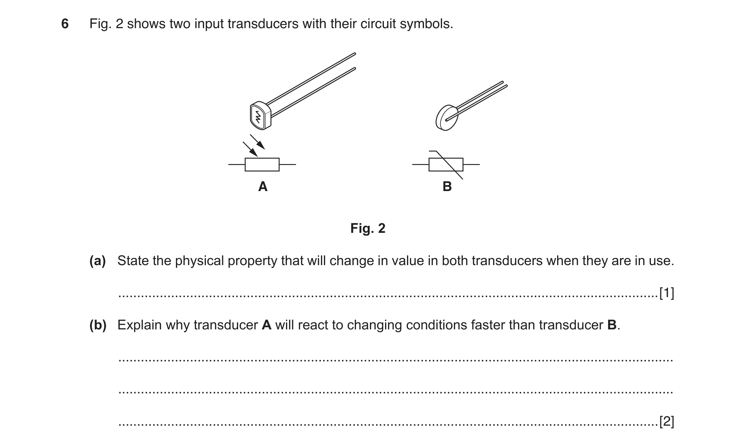 1 / 198
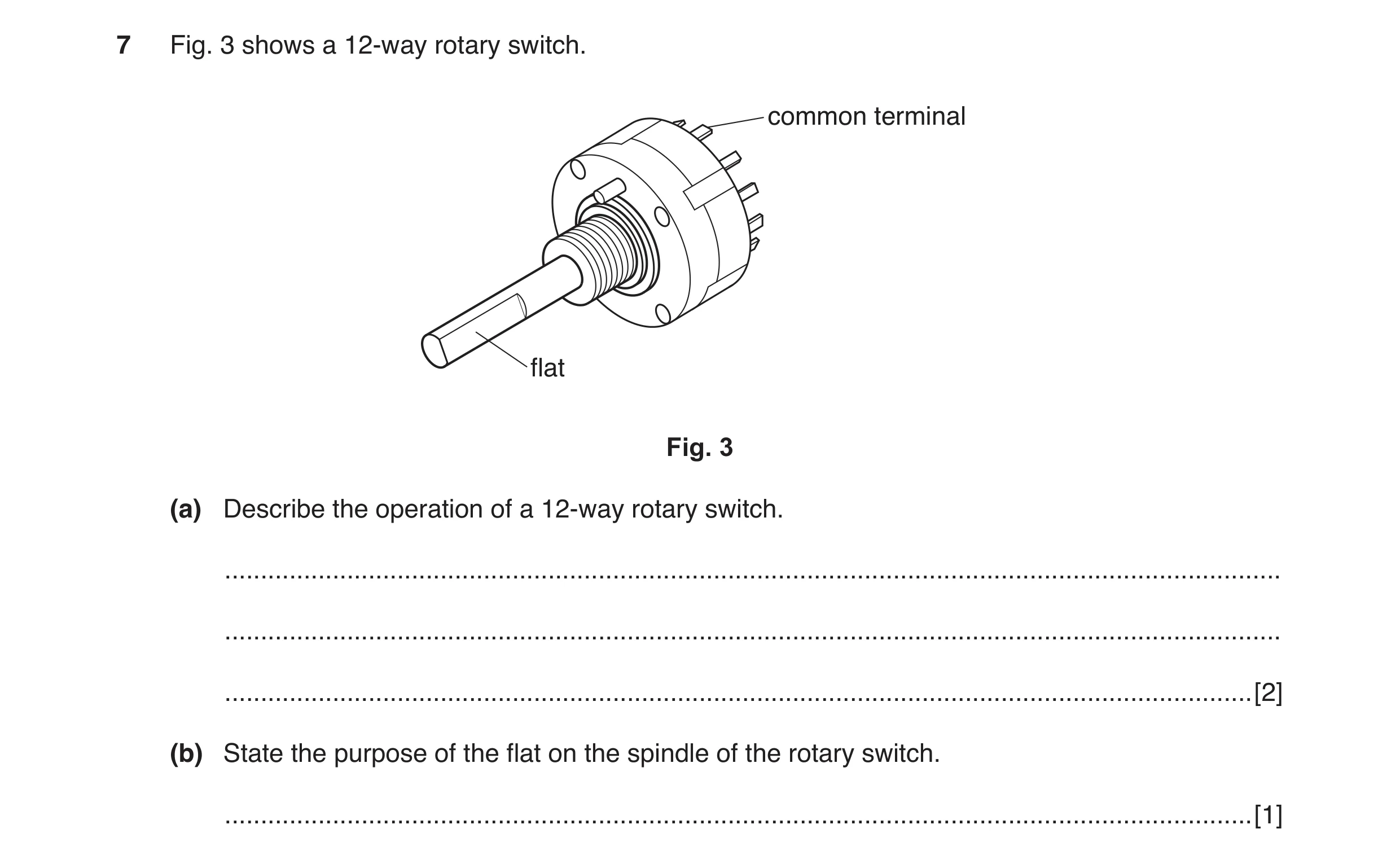 2 / 198
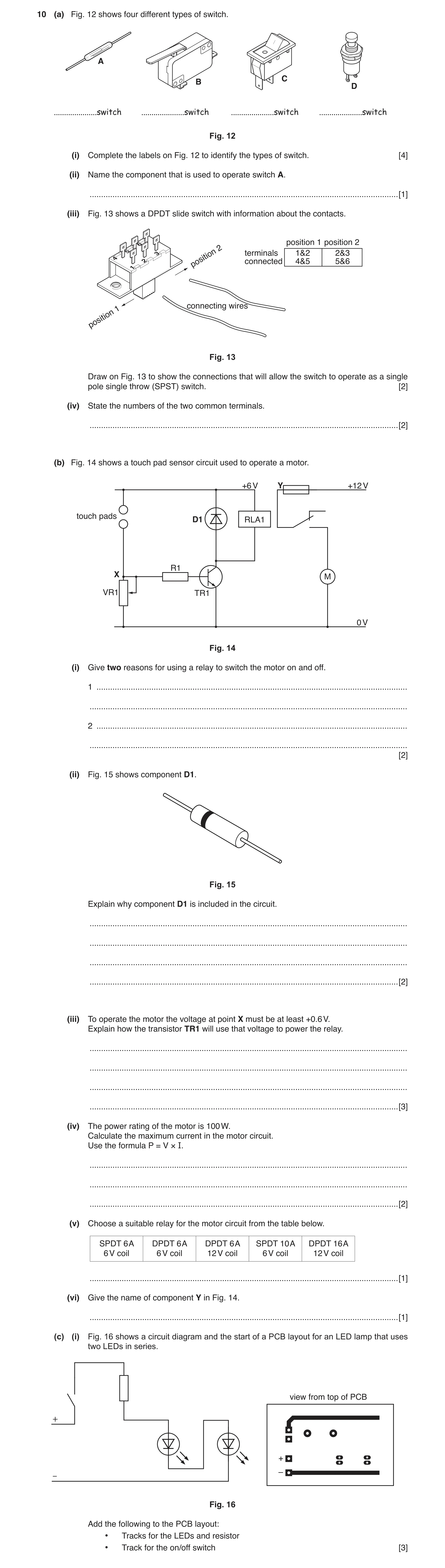
 10 / 198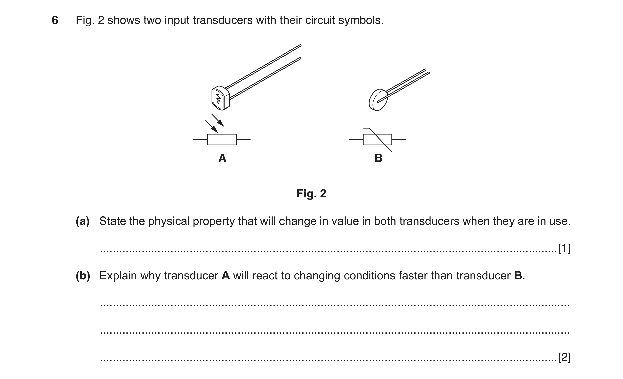
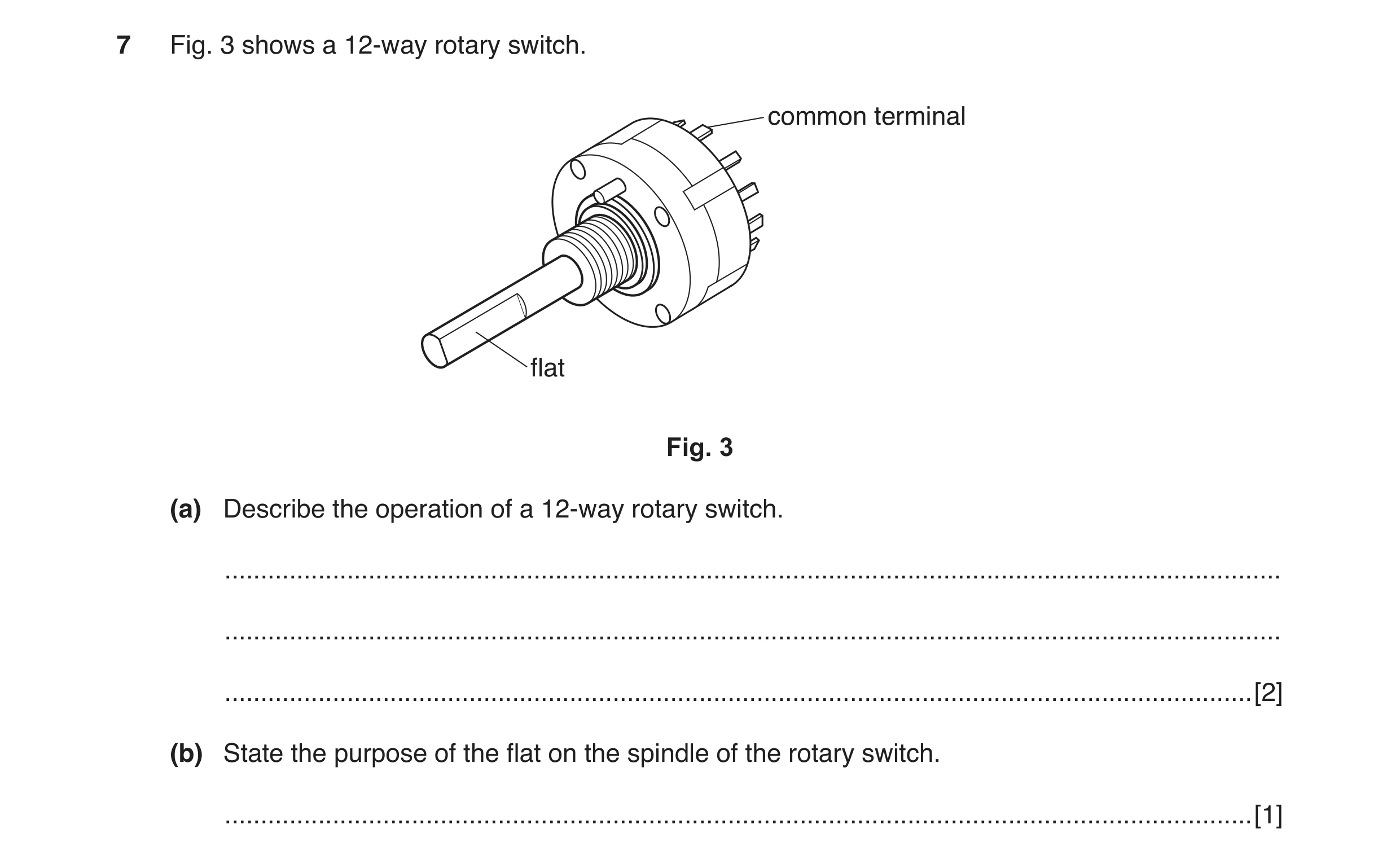 11 / 198
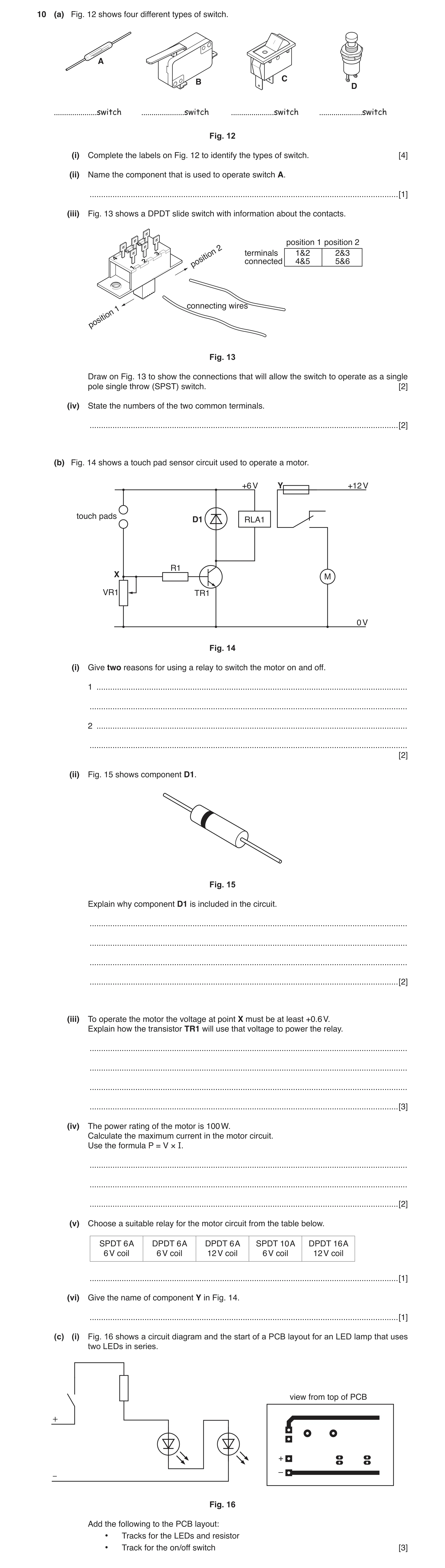
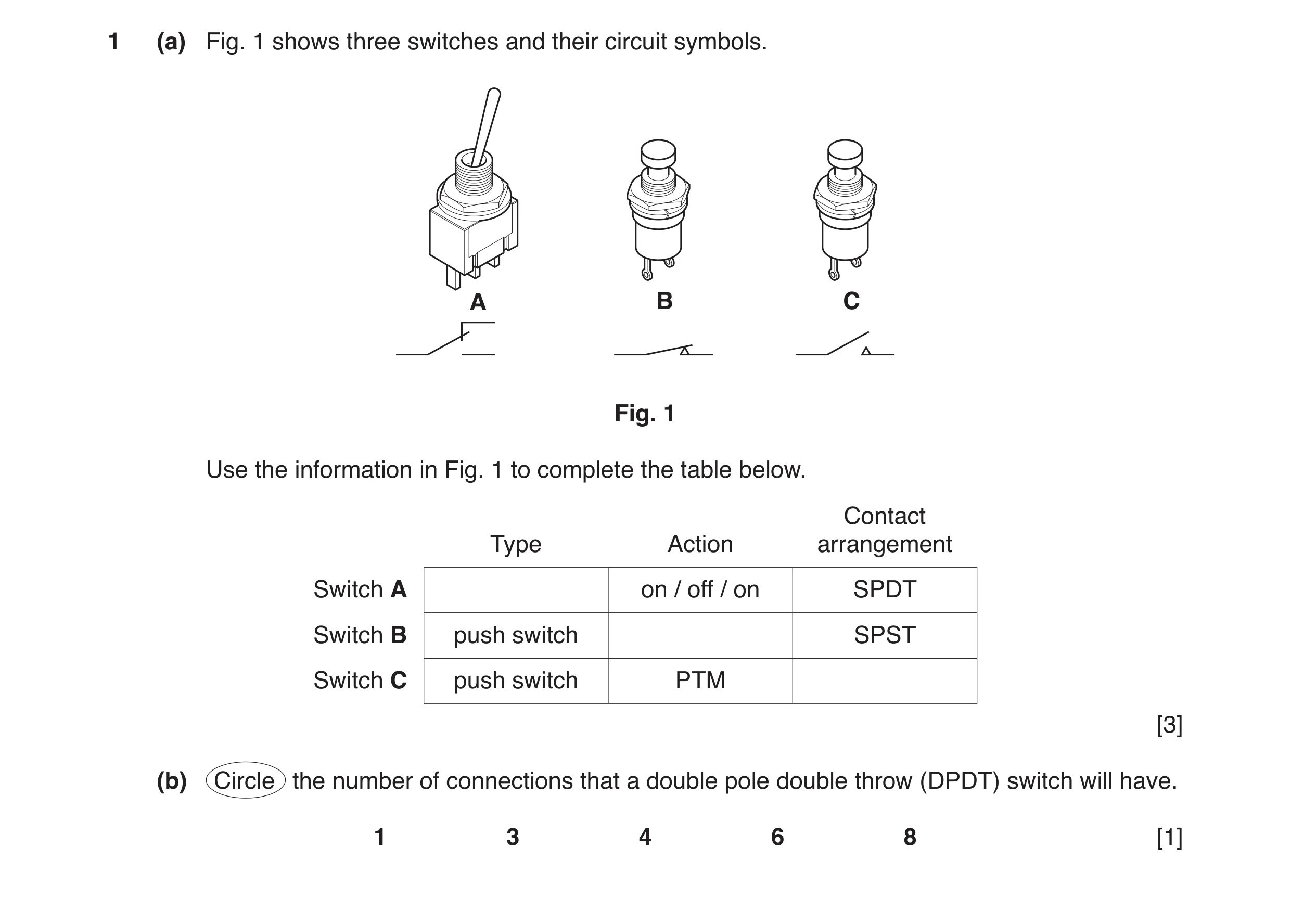
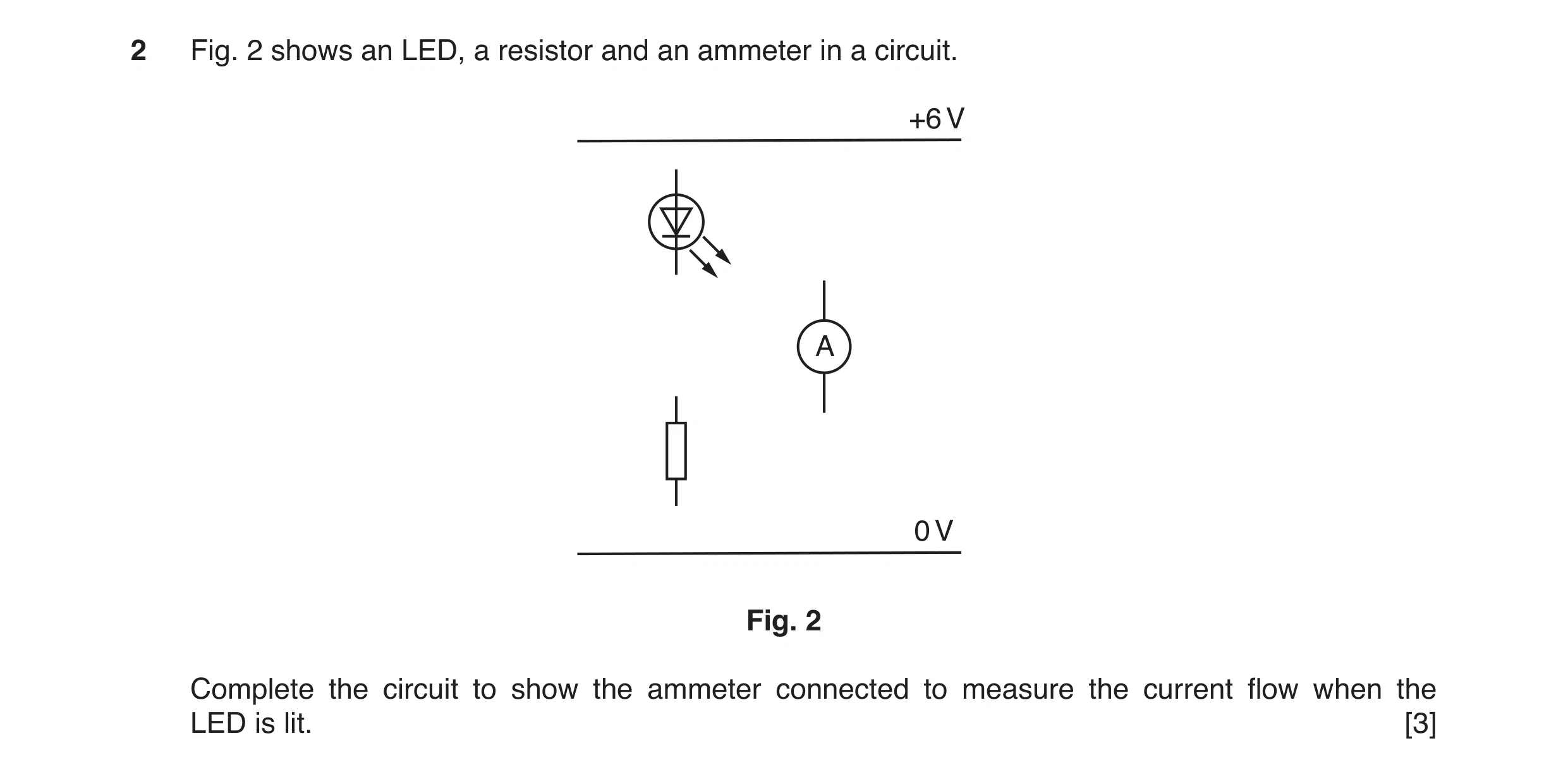 20 / 198
 21 / 198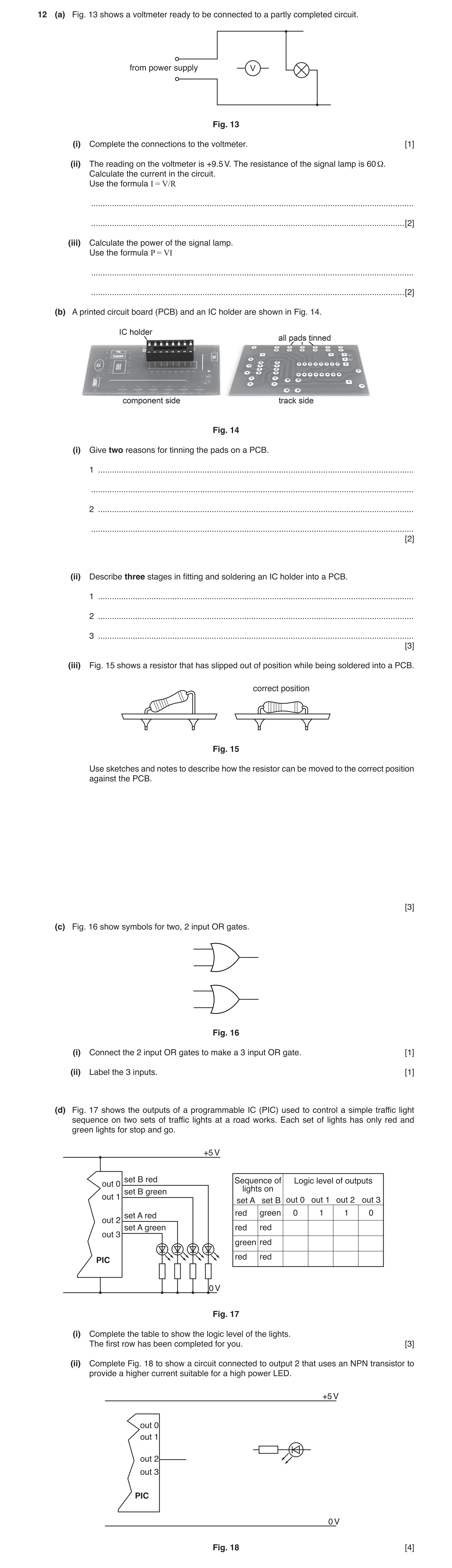
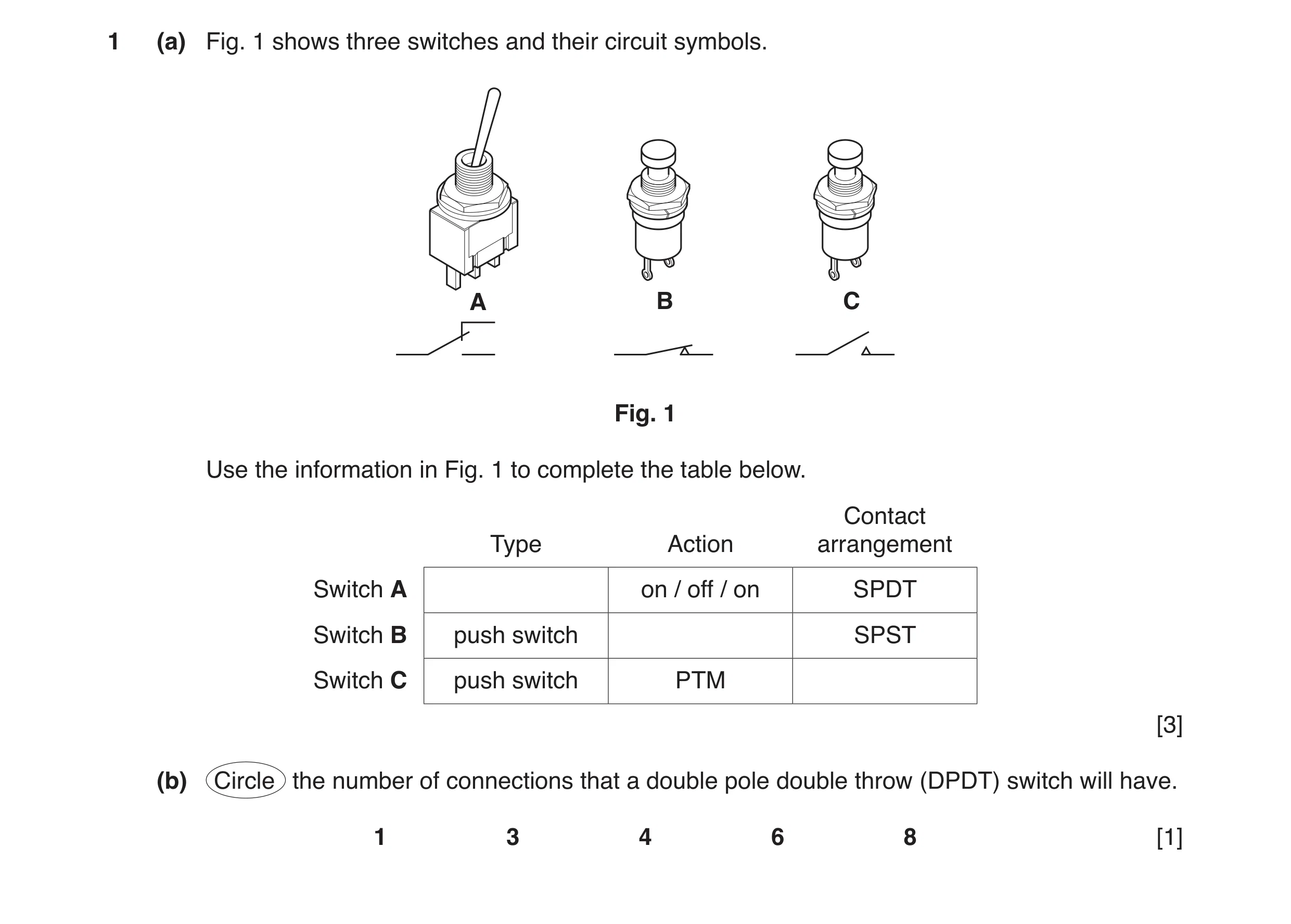
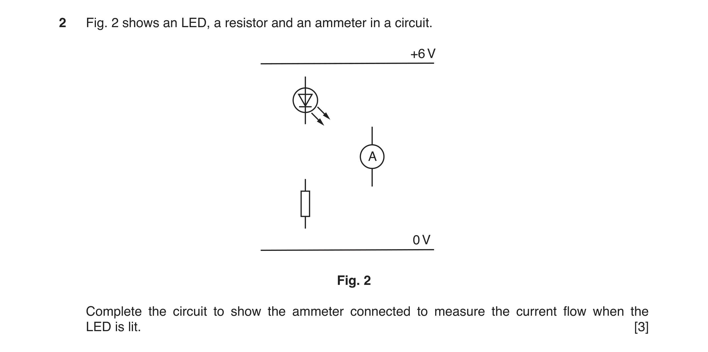 24 / 198
 25 / 198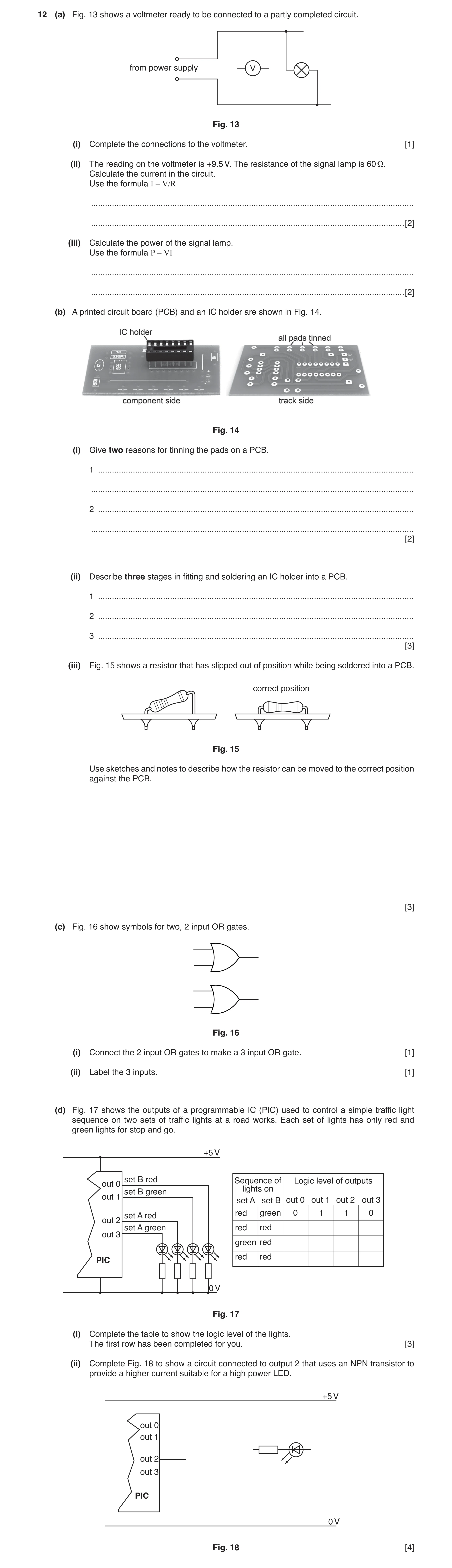
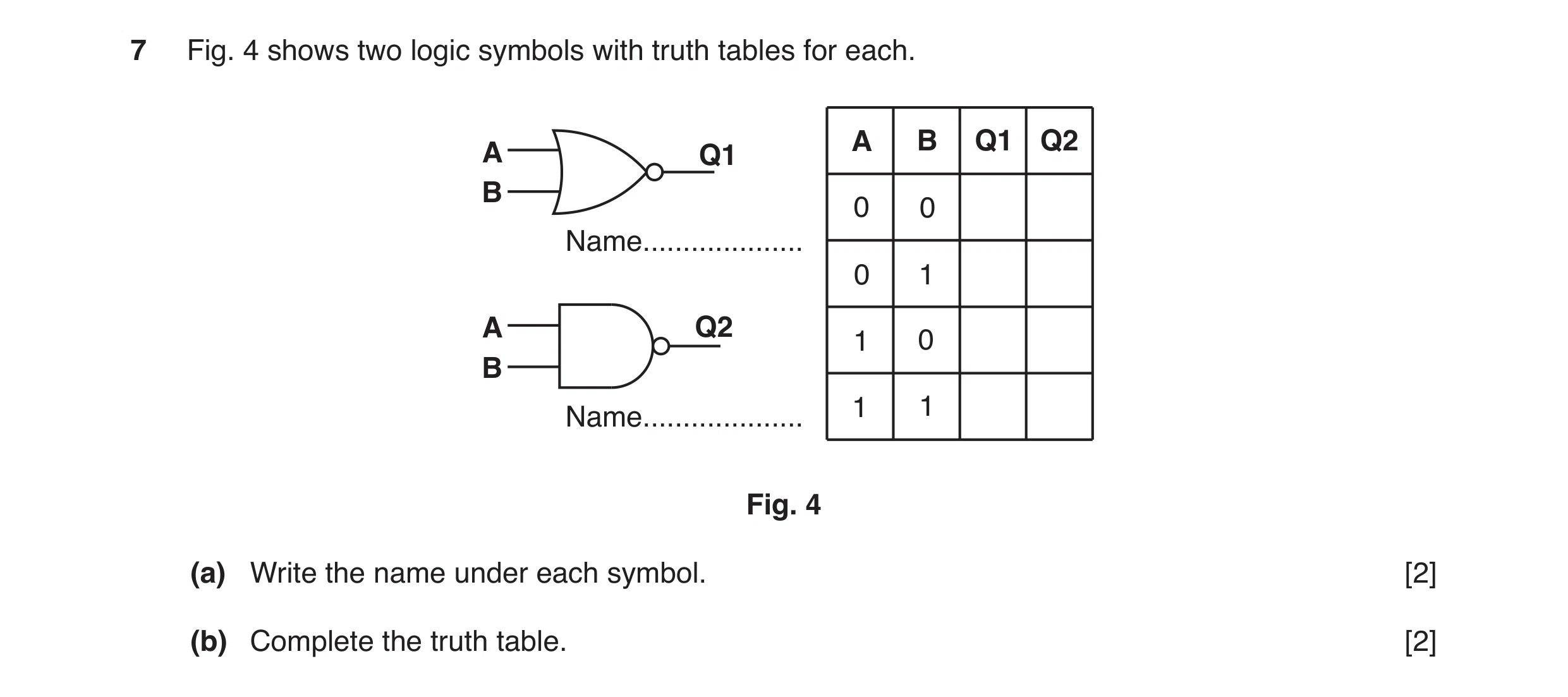
 28 / 198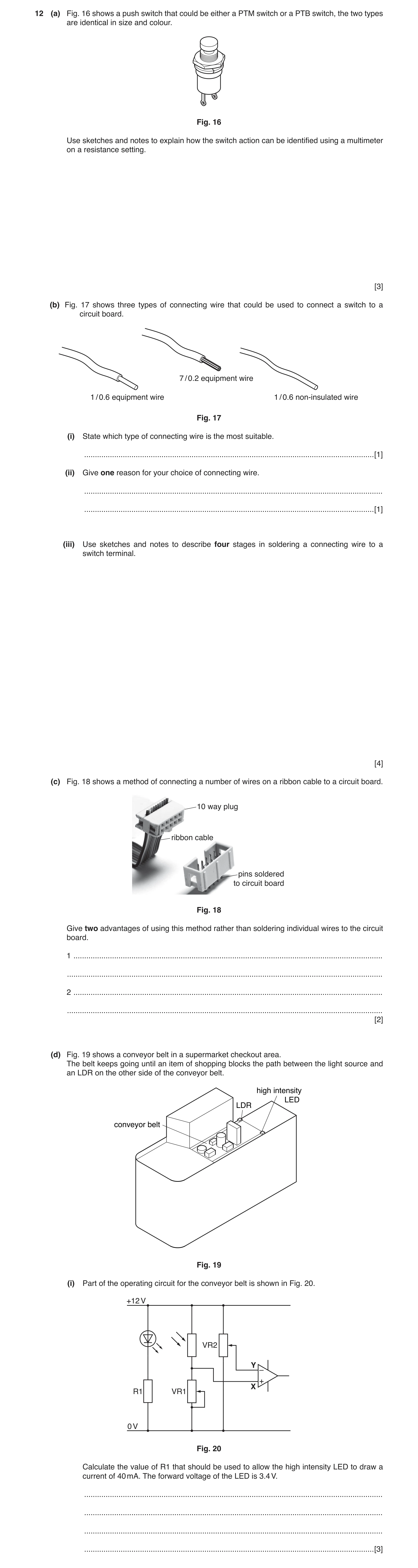
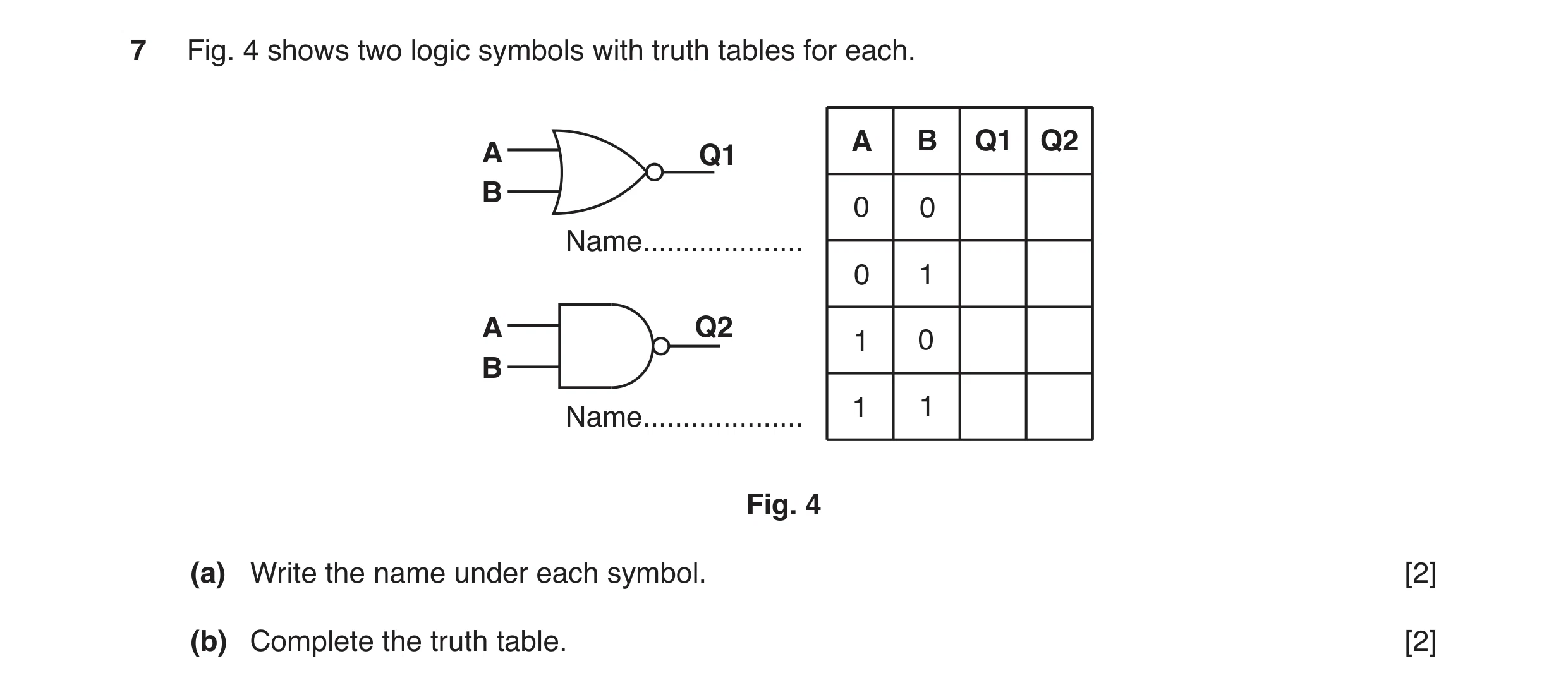
 32 / 198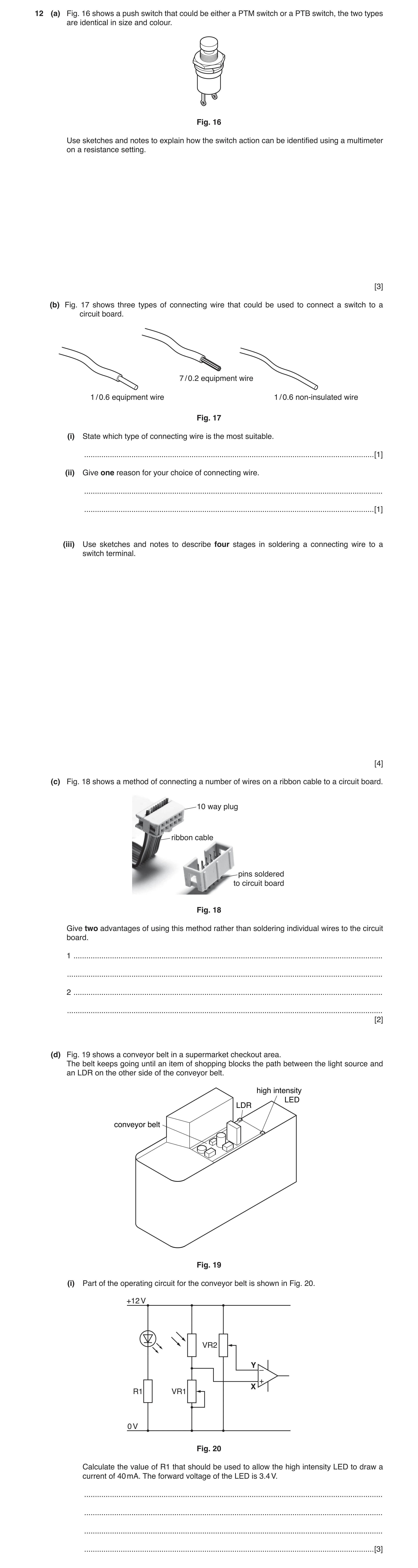
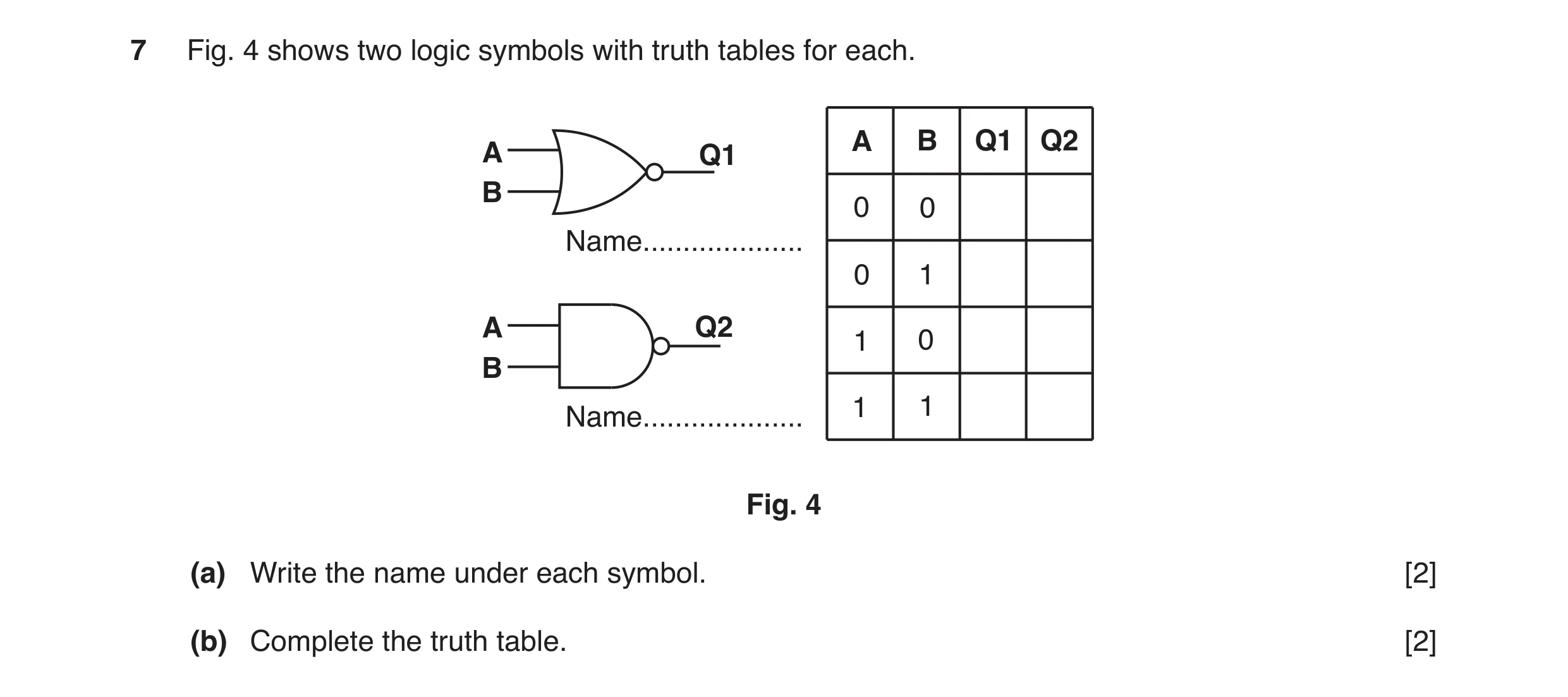
 36 / 198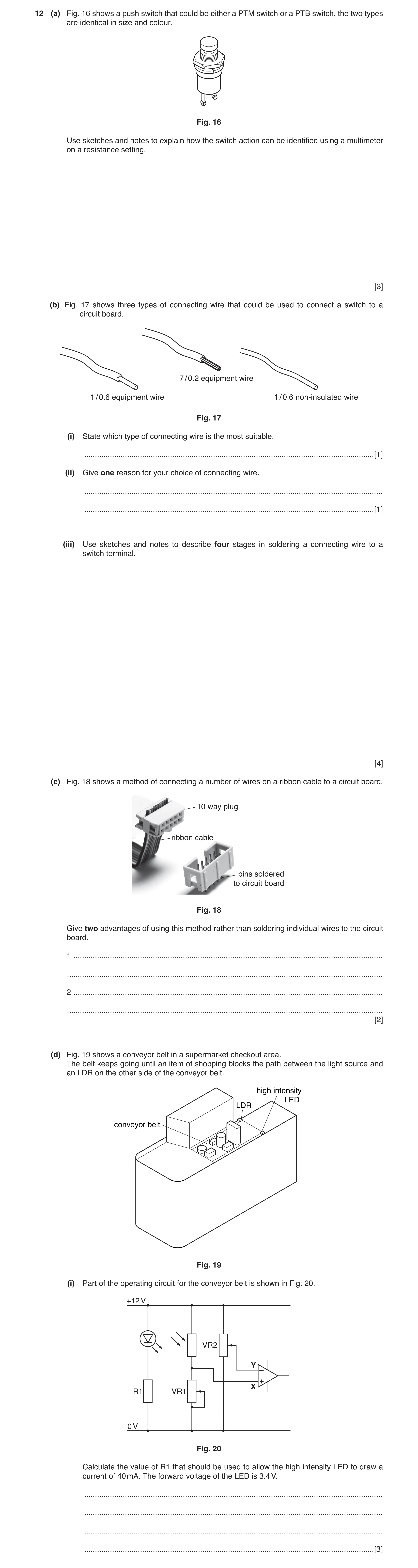
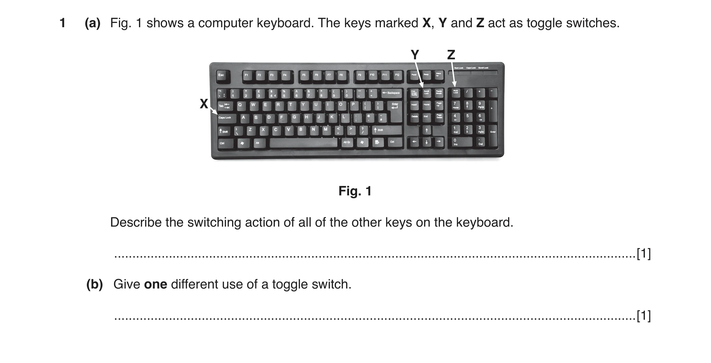
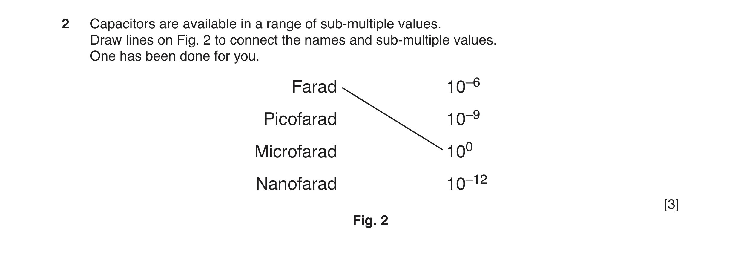
![Question 33: In the space below draw the following electronic symbols: Conductors crossing Conductors joined Alternating current [3]](https://img.pastlit.com/crops/ddef5d43-5b38-41be-9ea3-6fcdce9b0a58/q3.webp) 40 / 198
40 / 198 41 / 198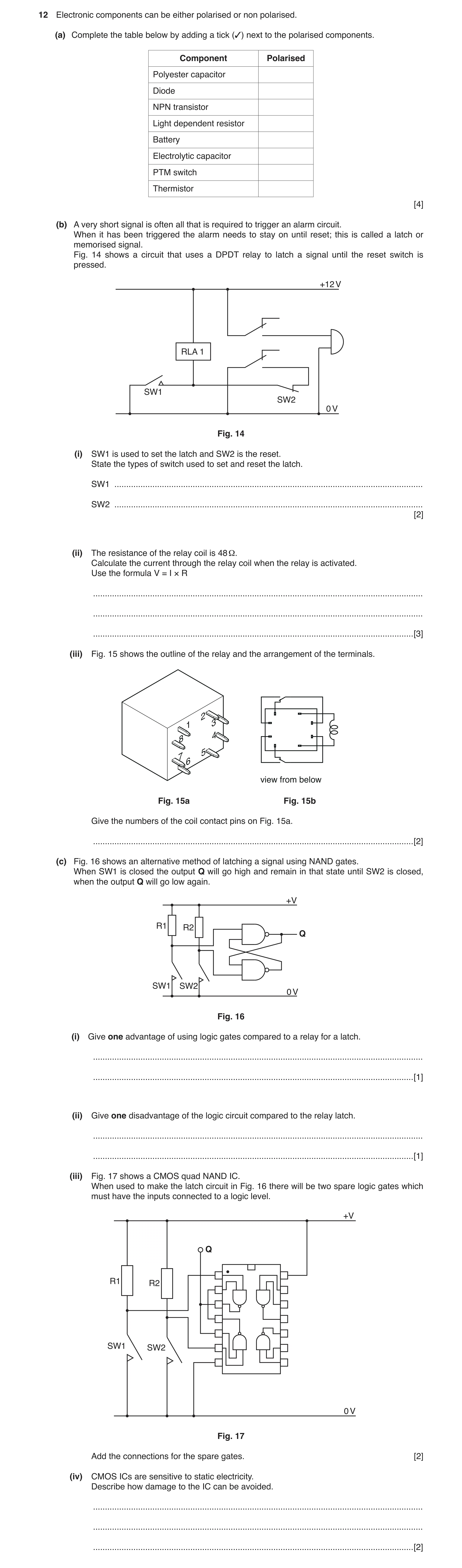
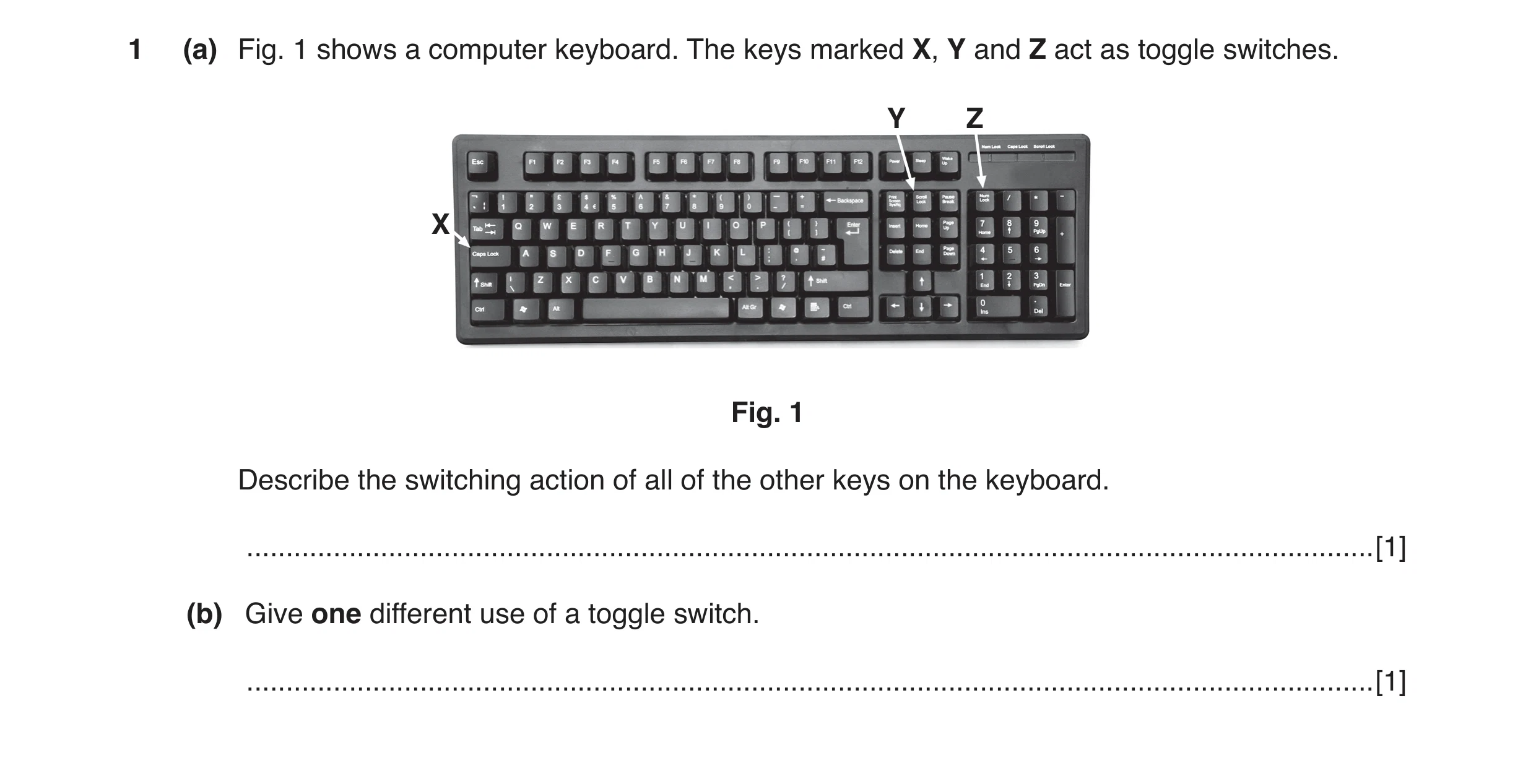
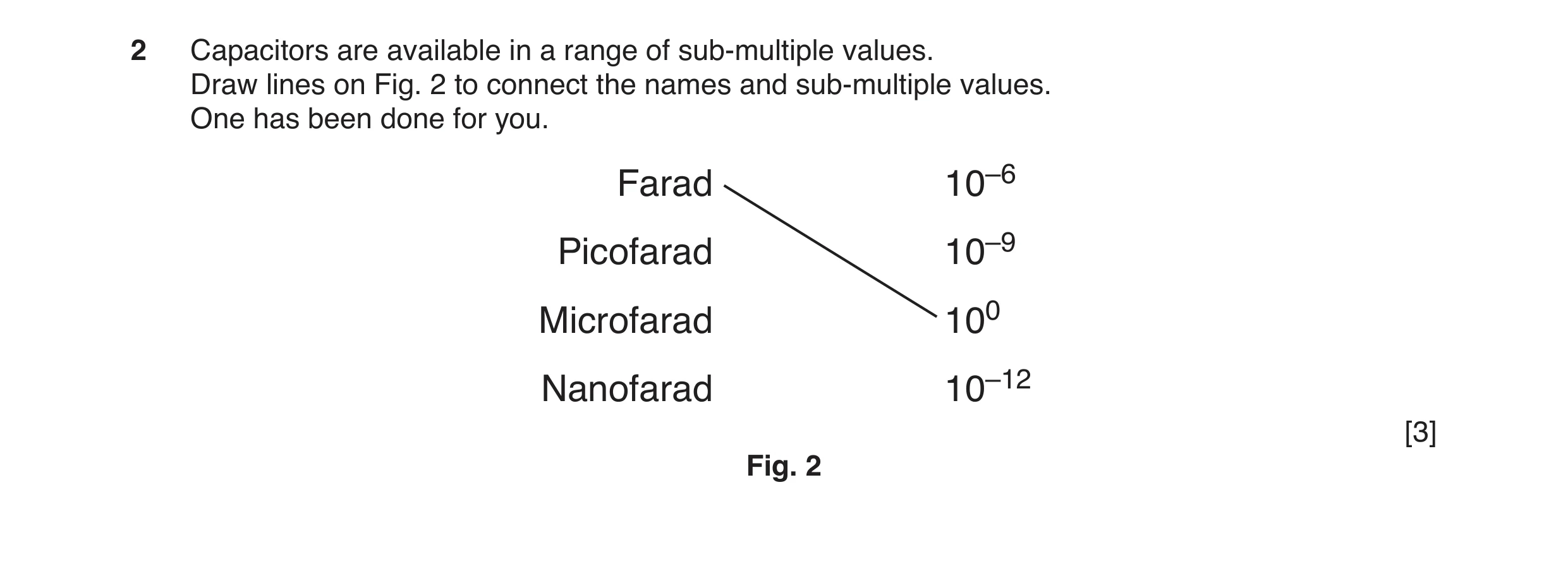
![Question 38: In the space below draw the following electronic symbols: Conductors crossing Conductors joined Alternating current [3]](https://img.pastlit.com/crops/540ffd47-95a5-4344-a9d0-caa8f86d65c9/q3.webp) 45 / 198
45 / 198 46 / 198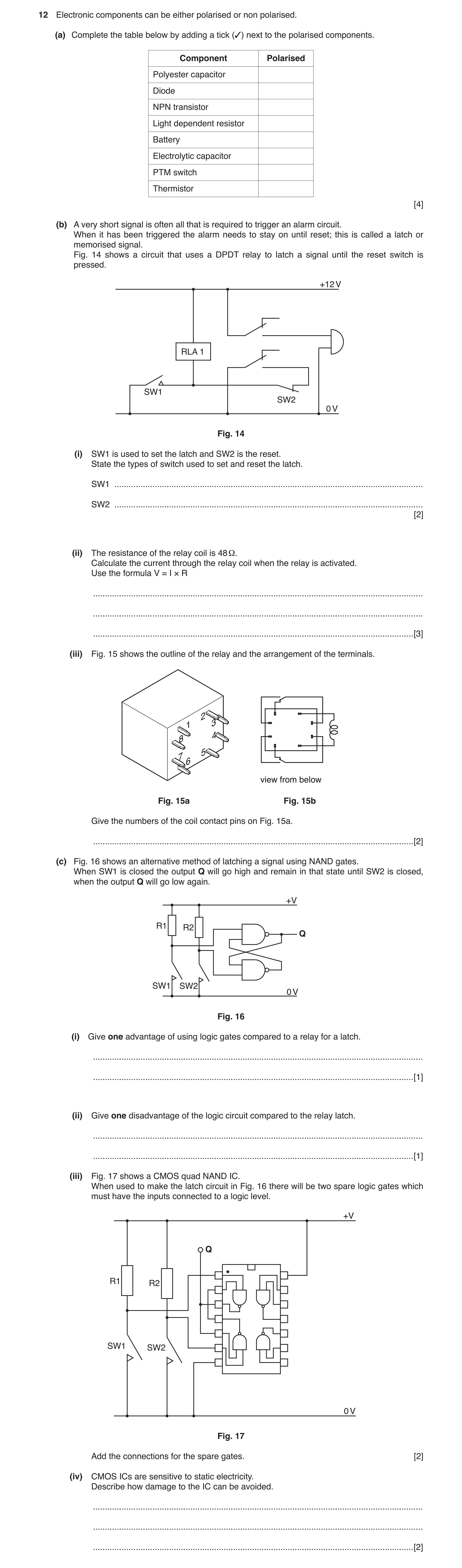
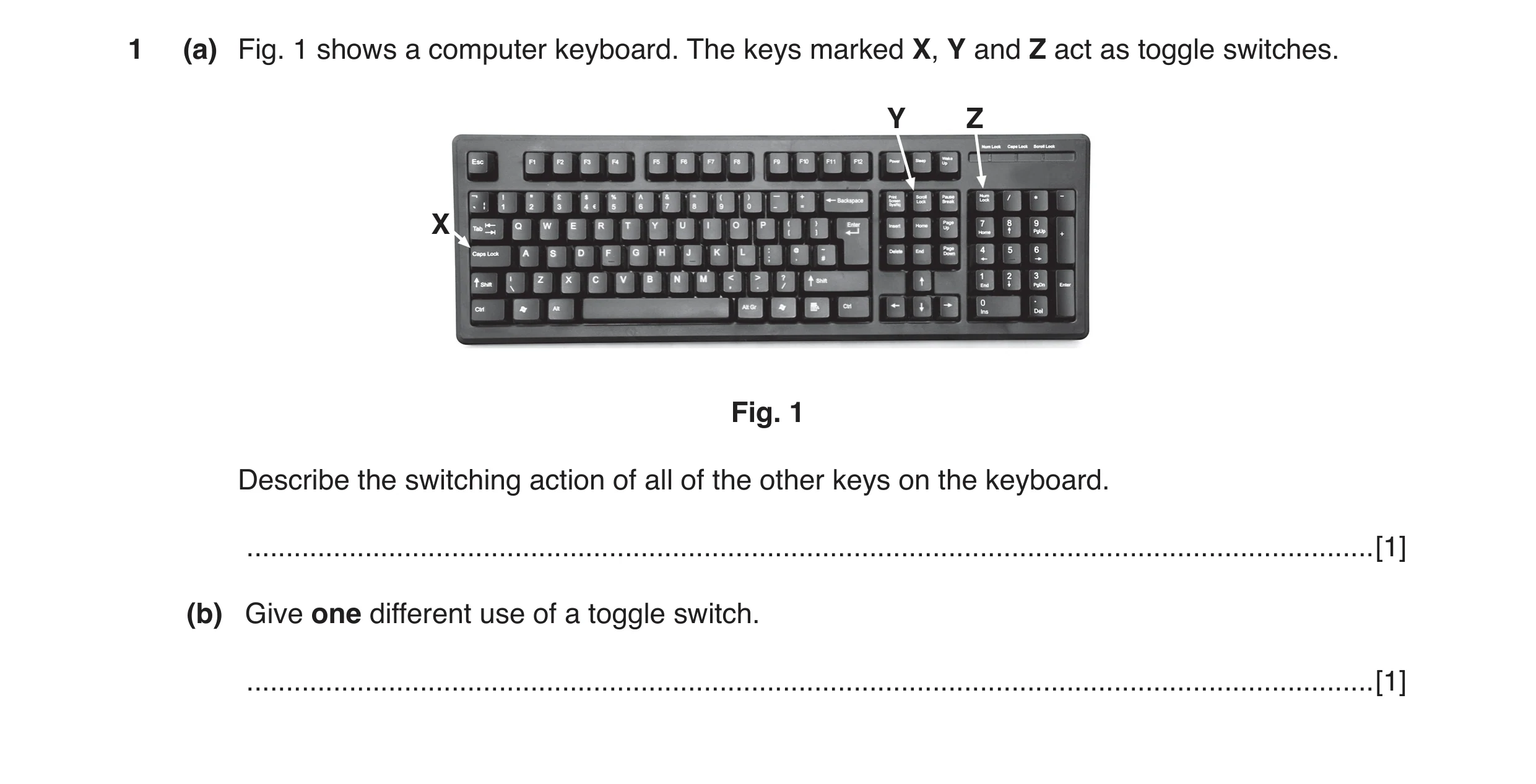
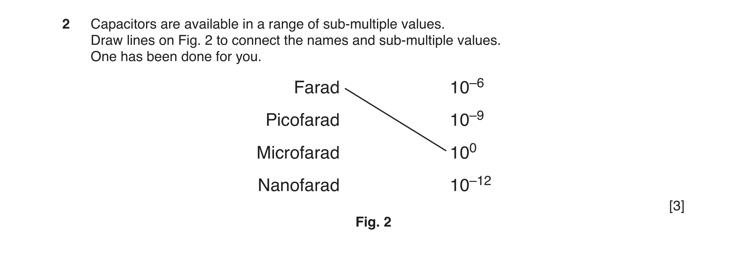
![Question 43: In the space below draw the following electronic symbols: Conductors crossing Conductors joined Alternating current [3]](https://img.pastlit.com/crops/3747dd33-af9b-413b-92ec-ba985cf5f1b9/q3.webp) 50 / 198
50 / 198 51 / 198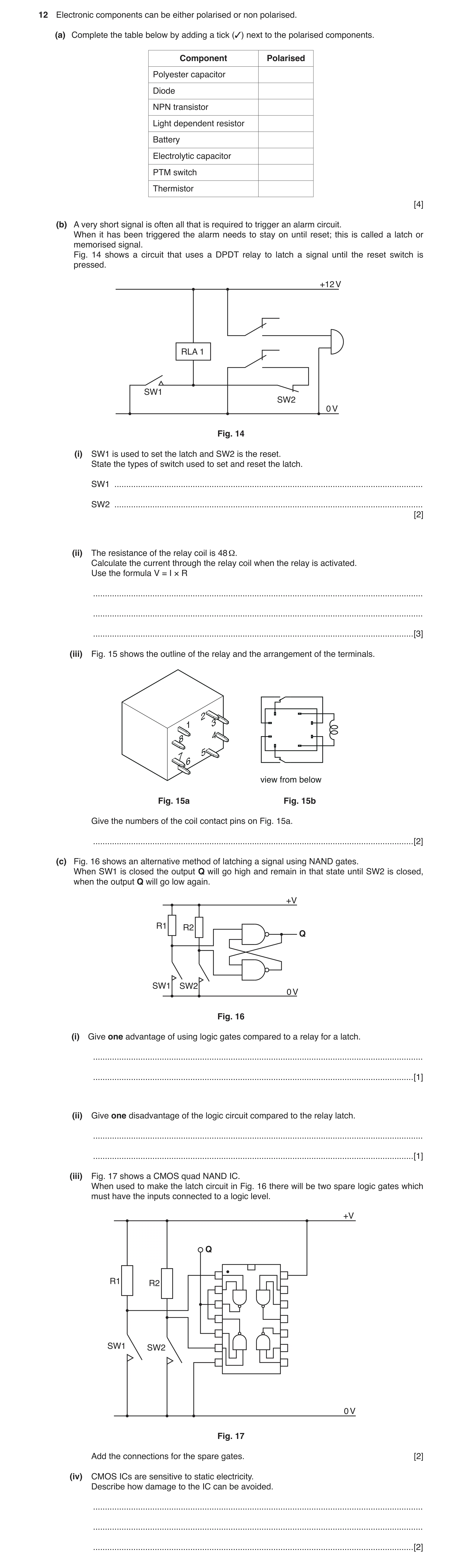
![Question 46: (a) Fig. 4 shows the outline of an IC. Fig. 4 Add pin numbers to the outline. [2] (b) Using the data in the table state the number of the I…](https://img.pastlit.com/crops/aa9d6010-0e0b-4034-b8ce-ceb0ab2951ac/q8.webp) 55 / 198
55 / 198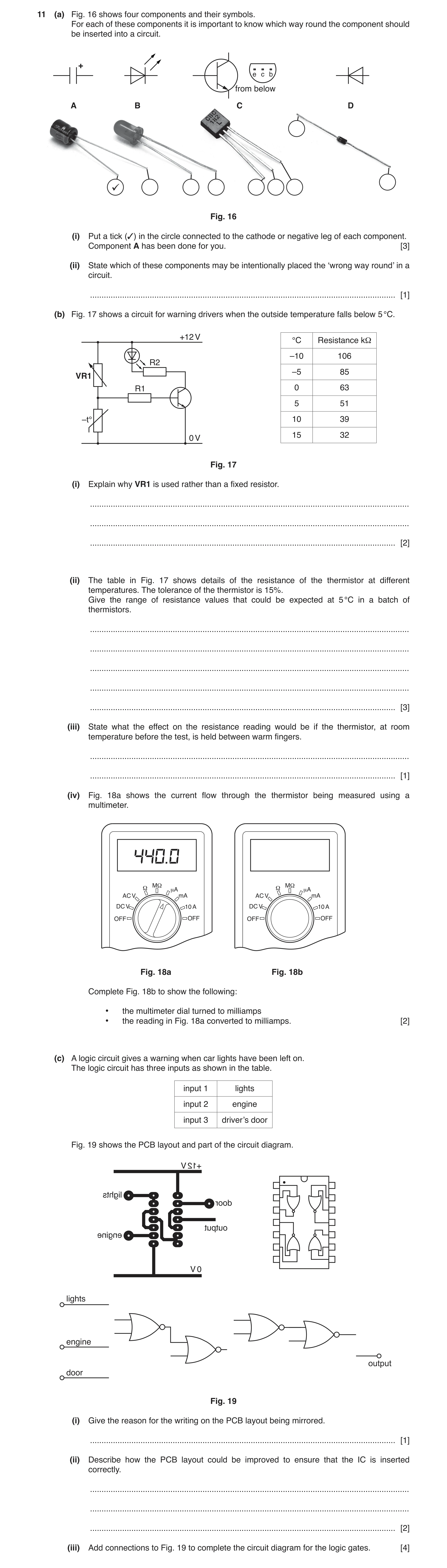
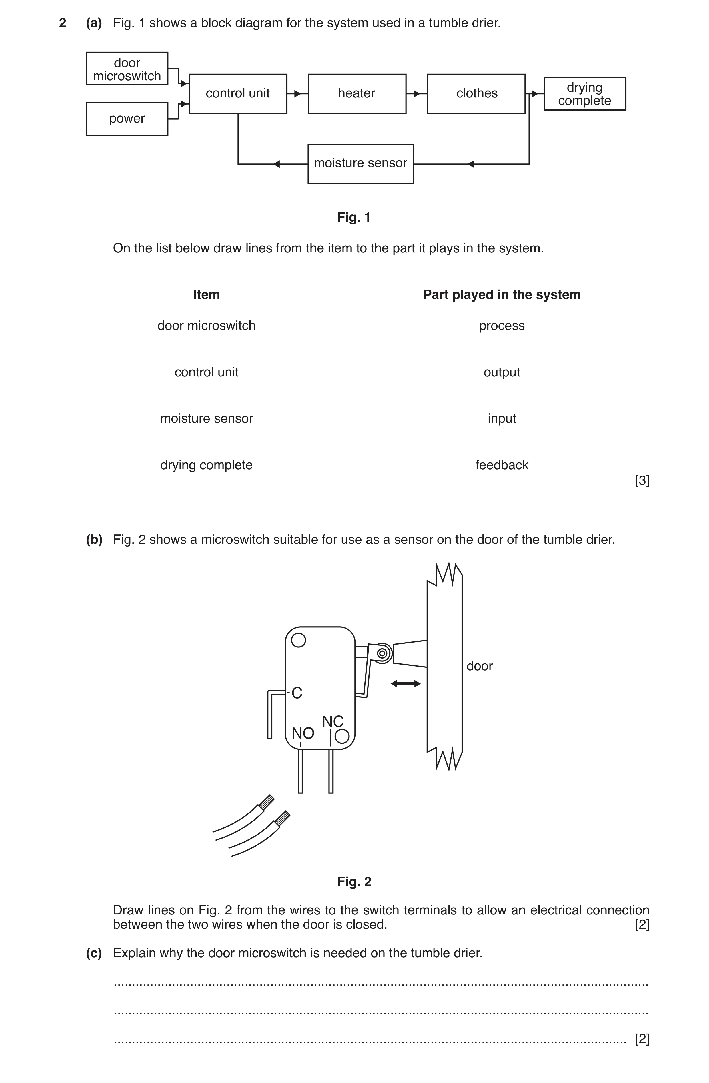
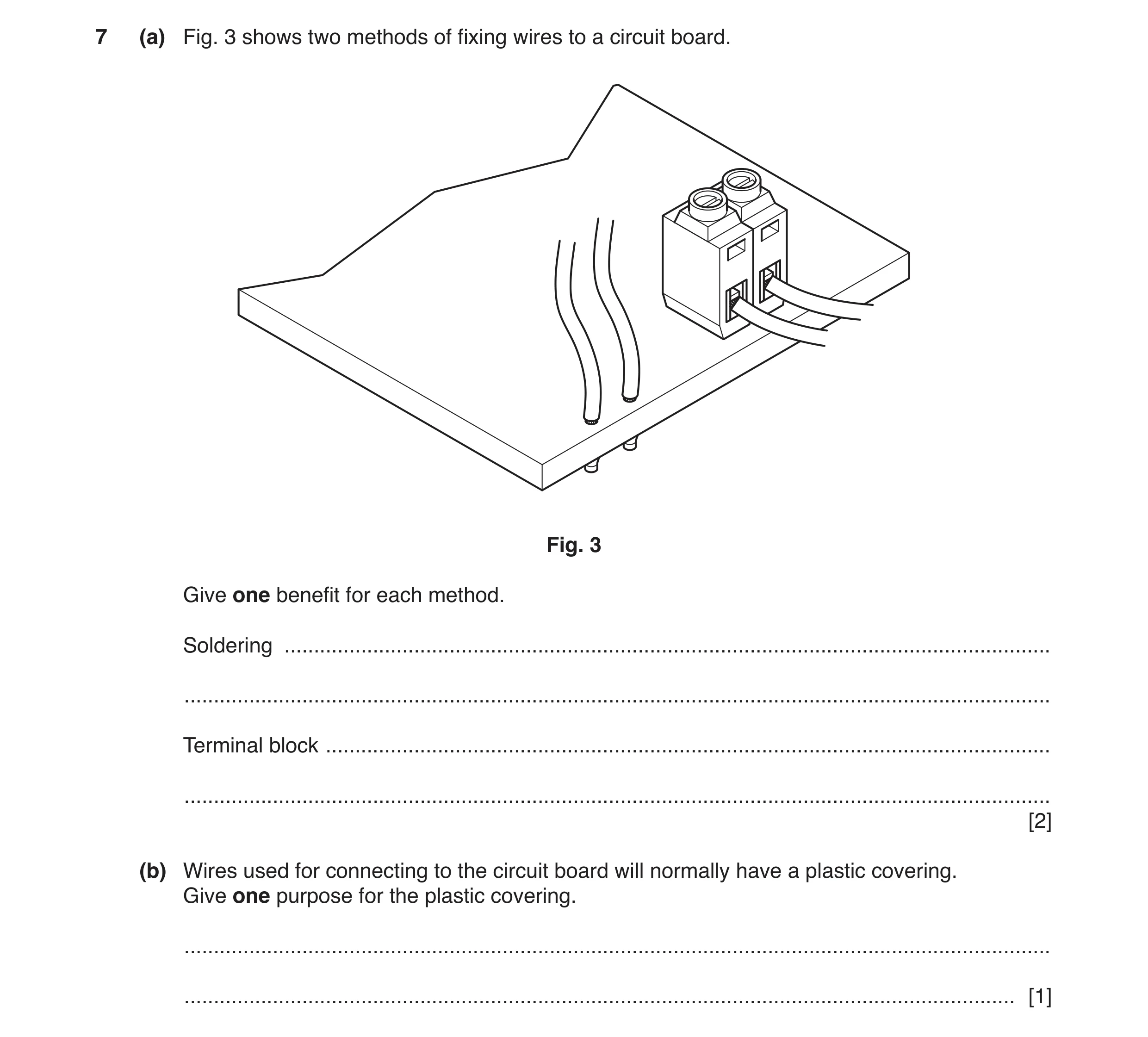 60 / 198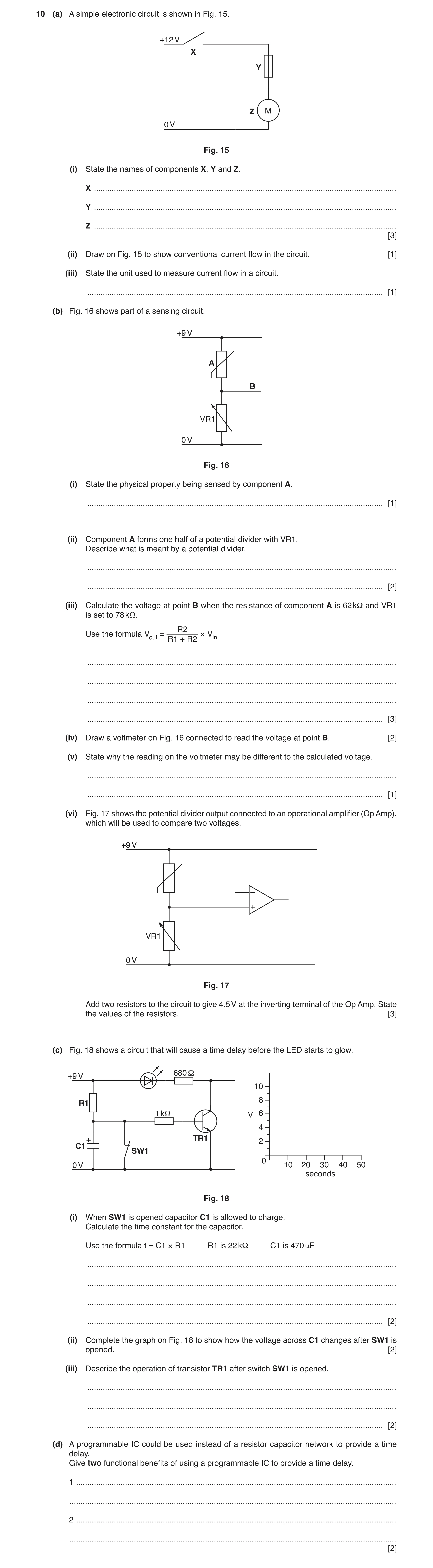
![Question 51: (a) Fig. 4 shows the outline of an IC. Fig. 4 Add pin numbers to the outline. [2] (b) Using the data in the table state the number of the I…](https://img.pastlit.com/crops/510e6998-9d7f-495f-9eca-d4a8536ab36d/q8.webp) 64 / 198
64 / 198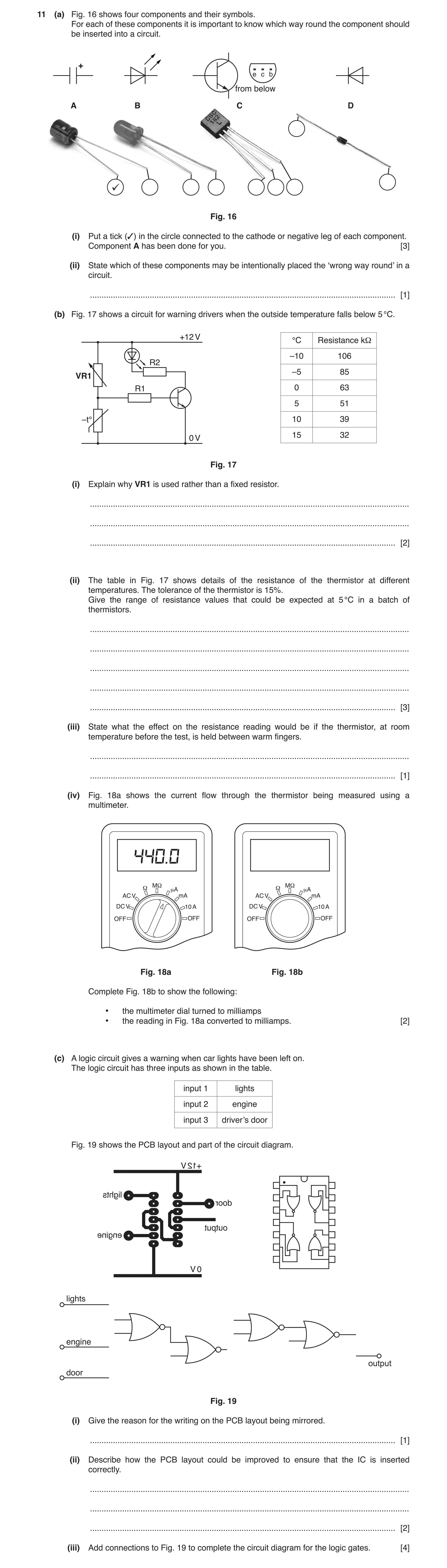
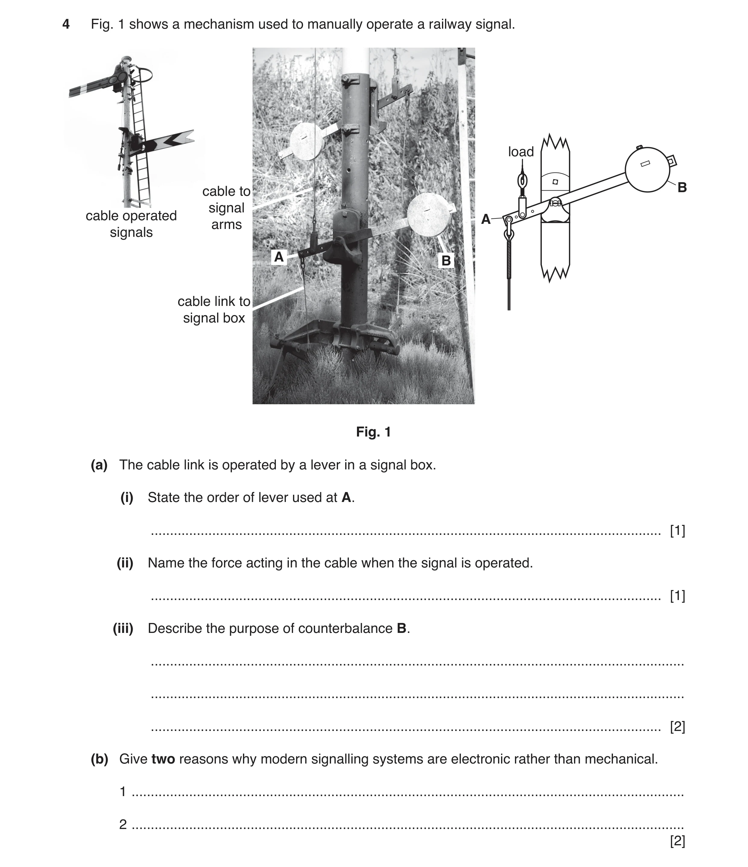 68 / 198

 69 / 198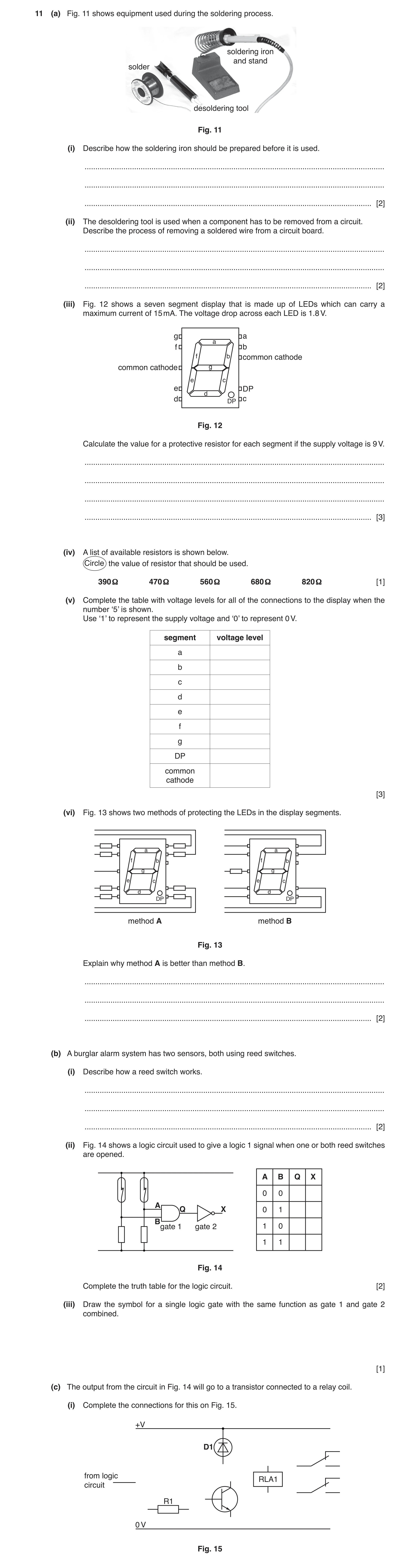
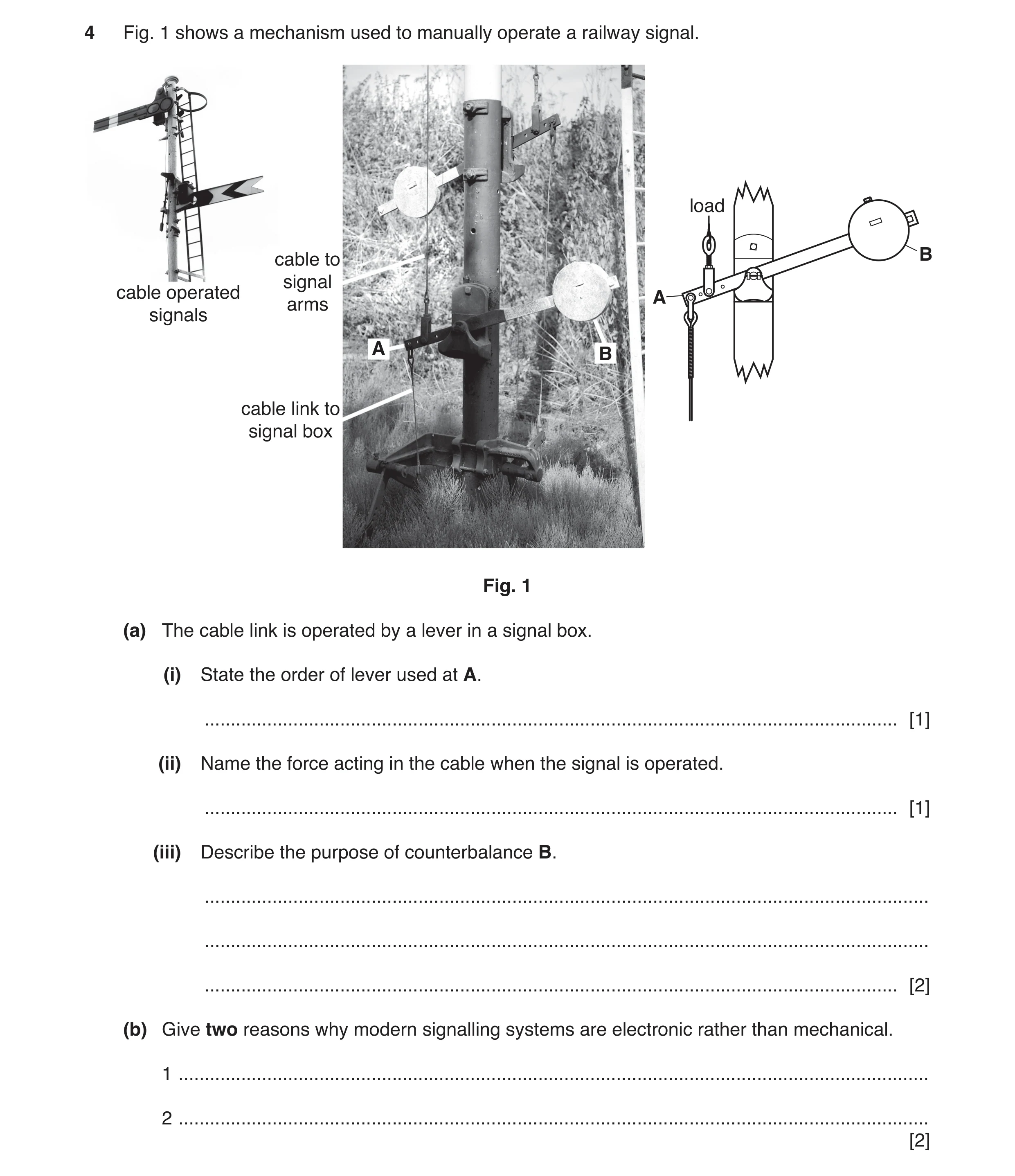 73 / 198

 74 / 198
 78 / 198

 79 / 198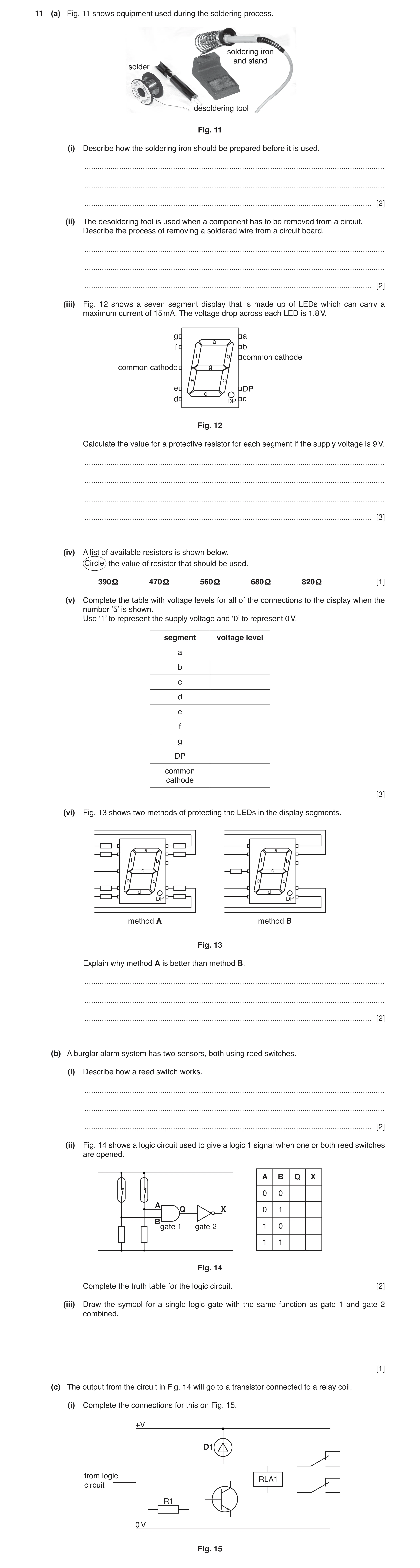
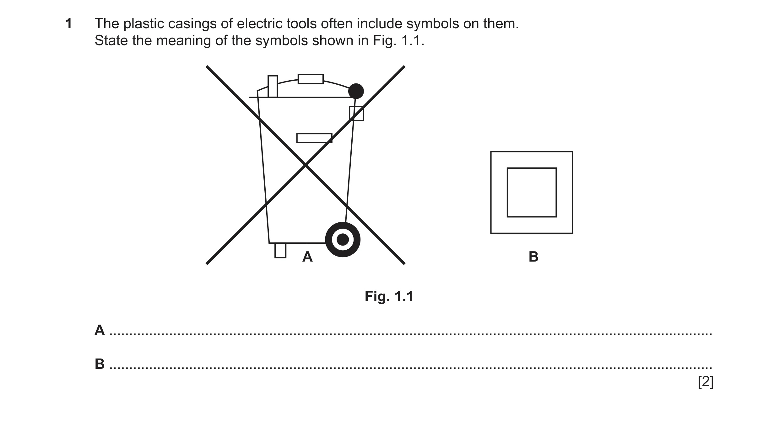
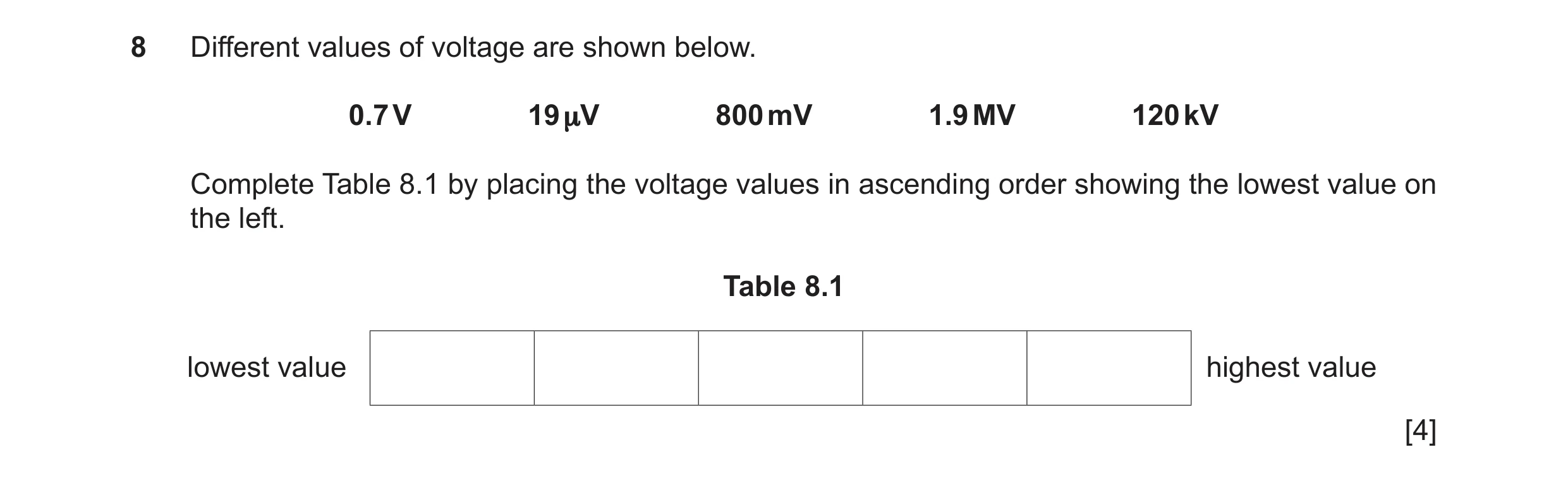
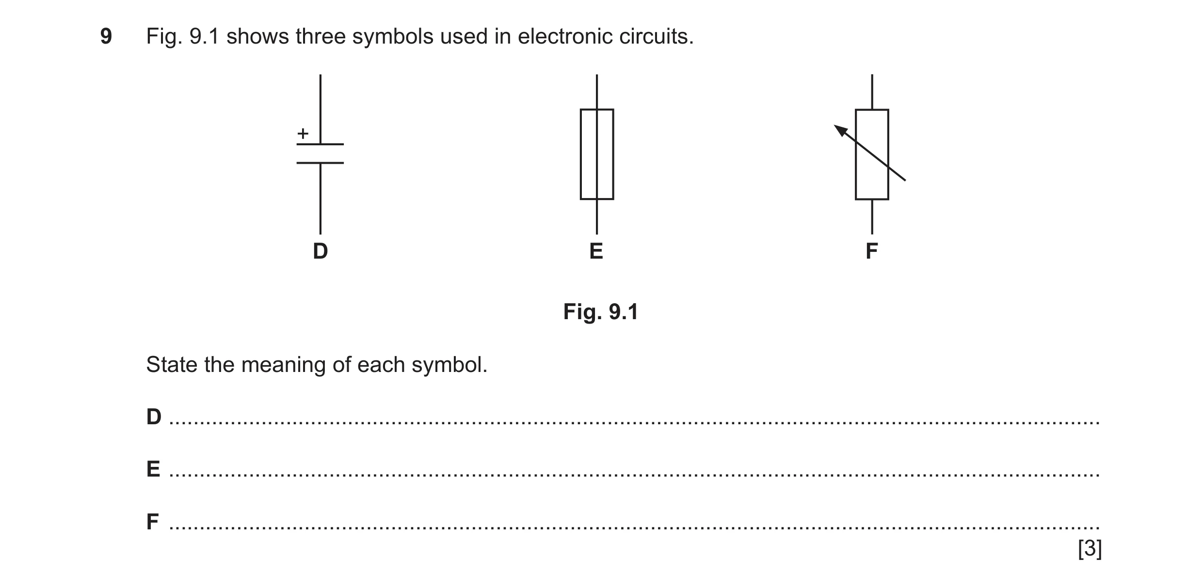 83 / 198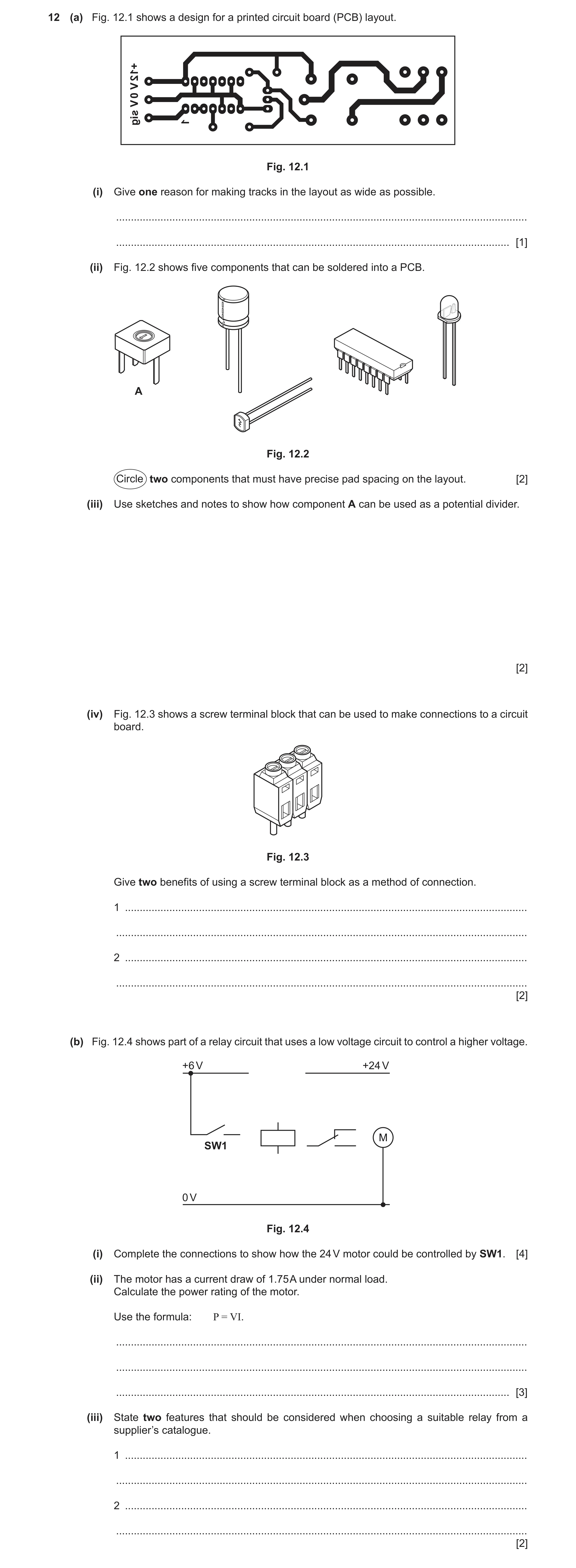
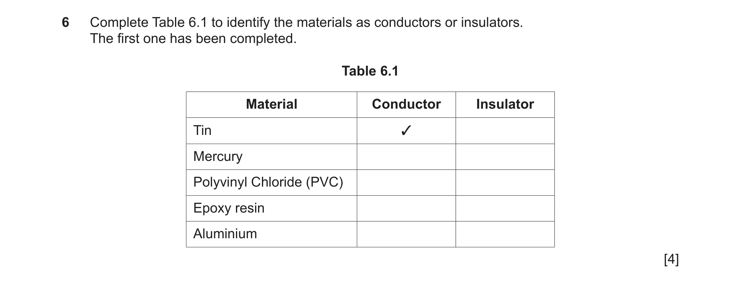
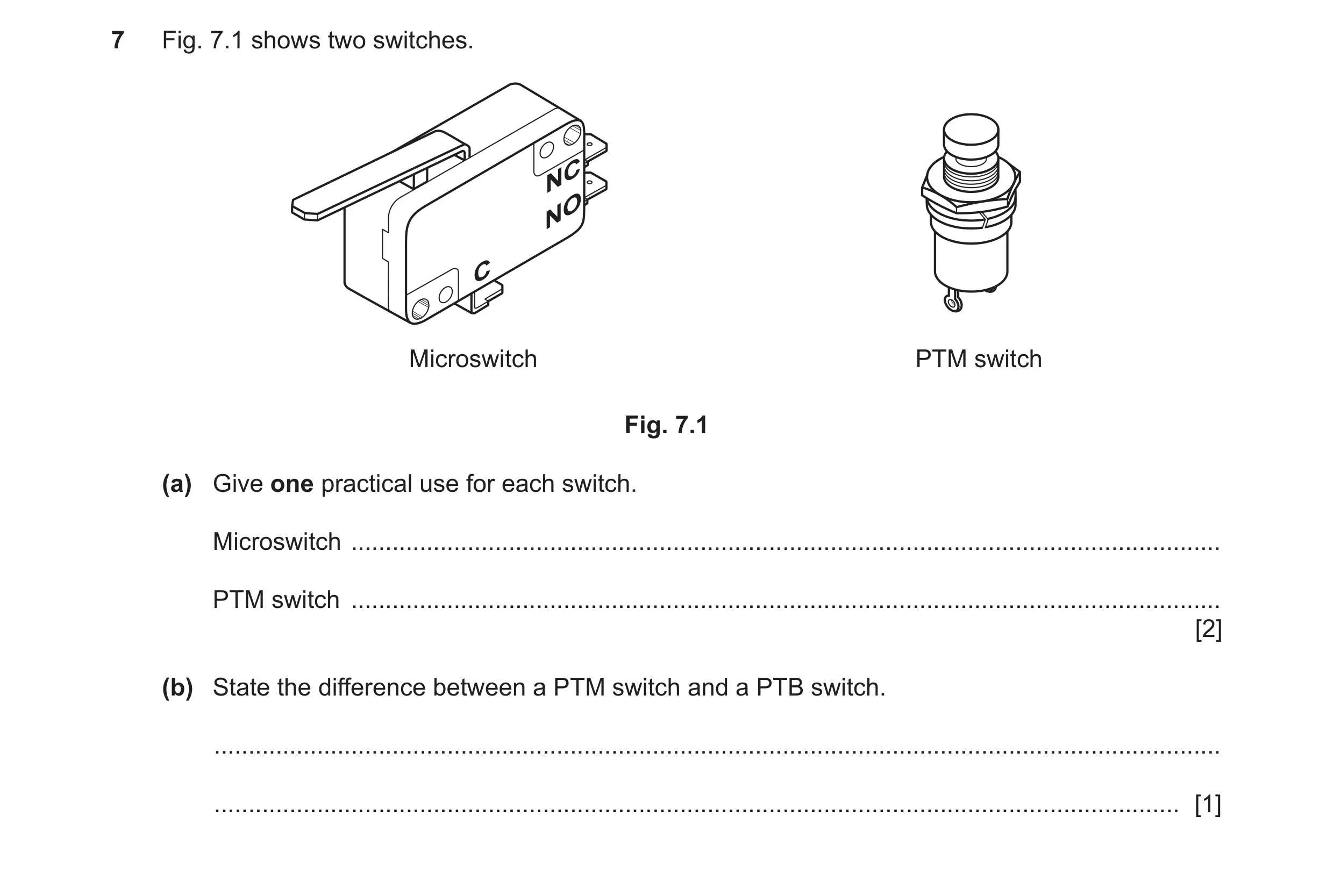 86 / 198
 87 / 198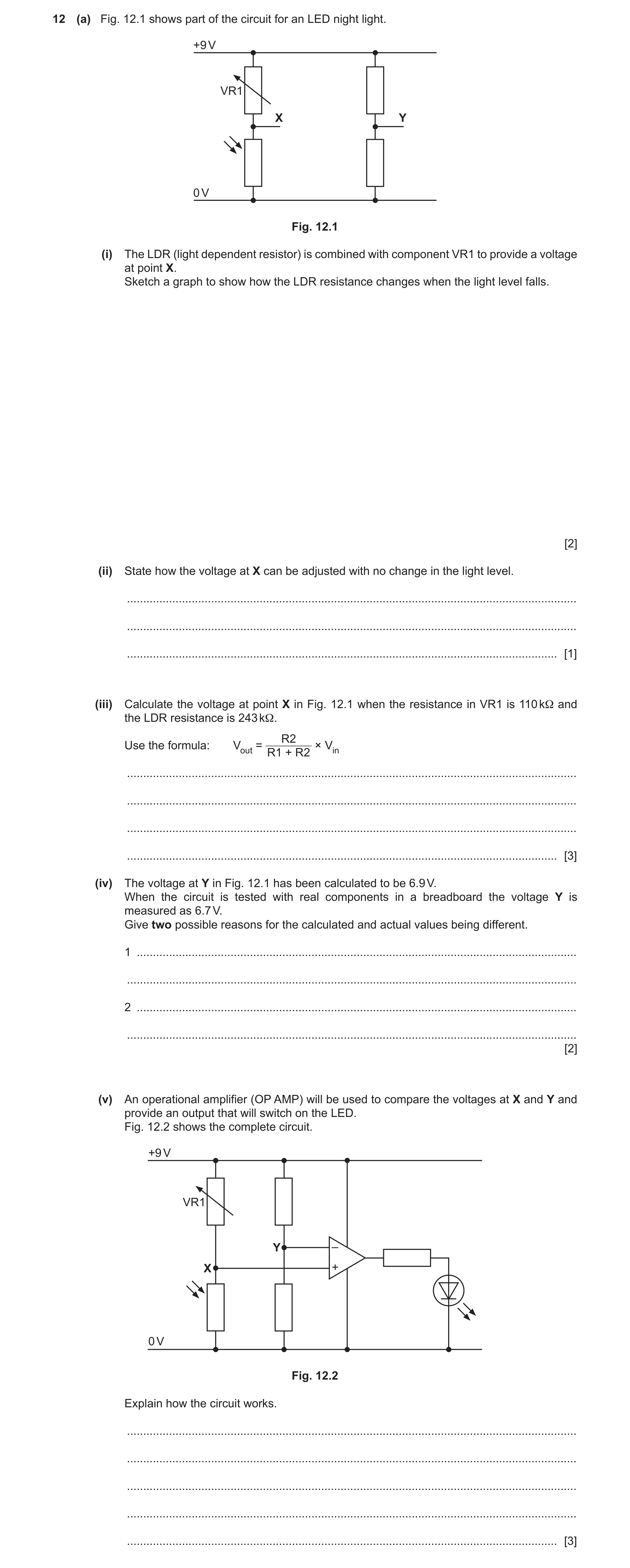
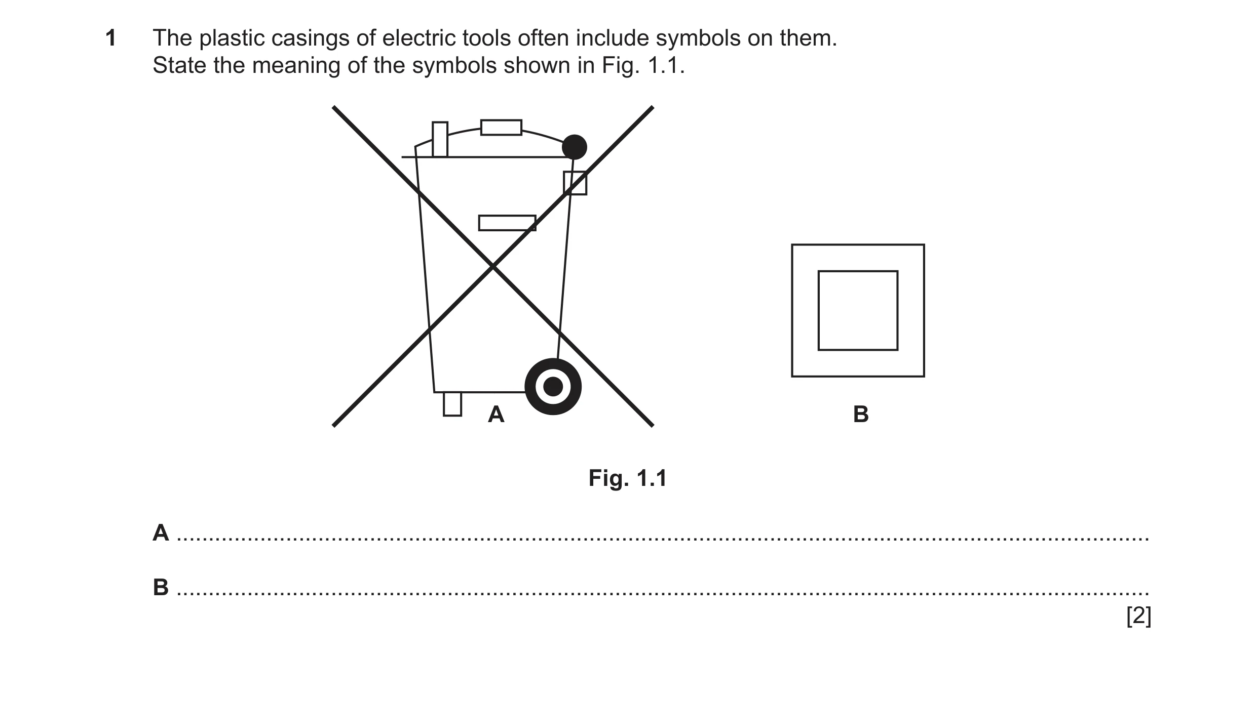
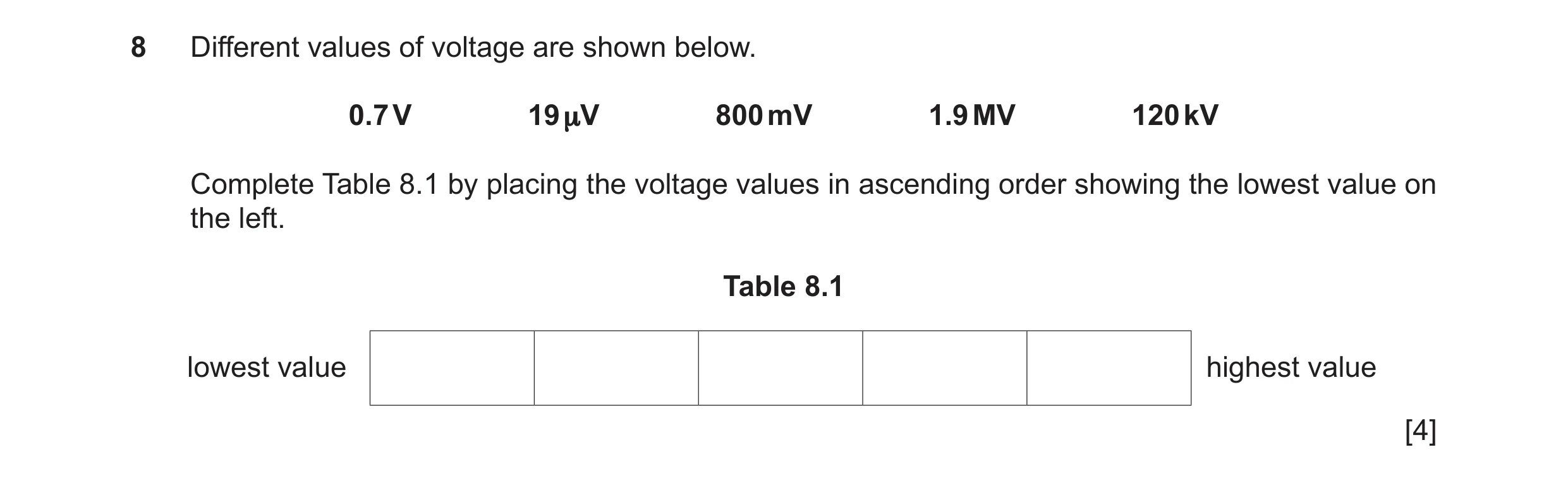
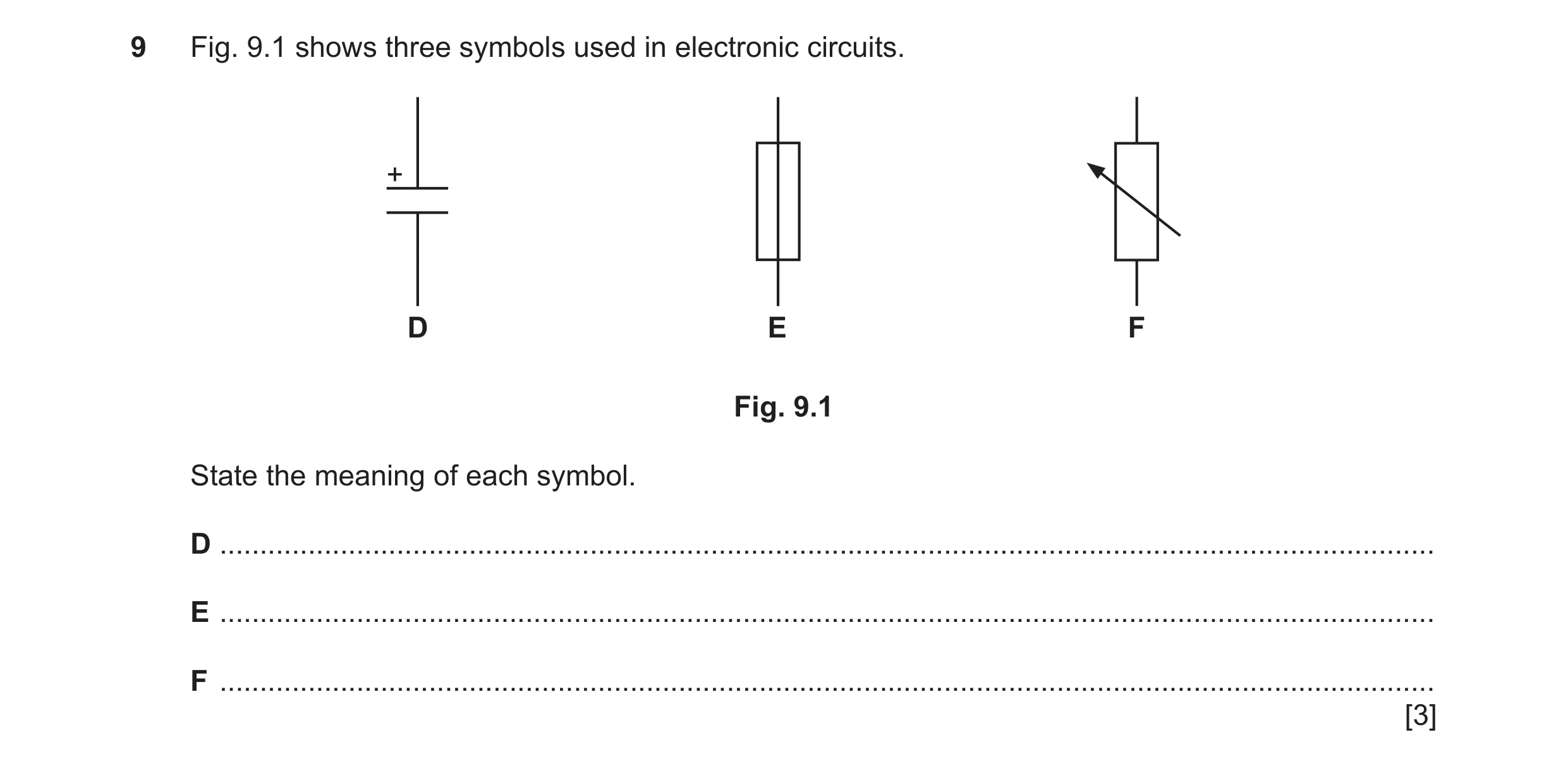 89 / 198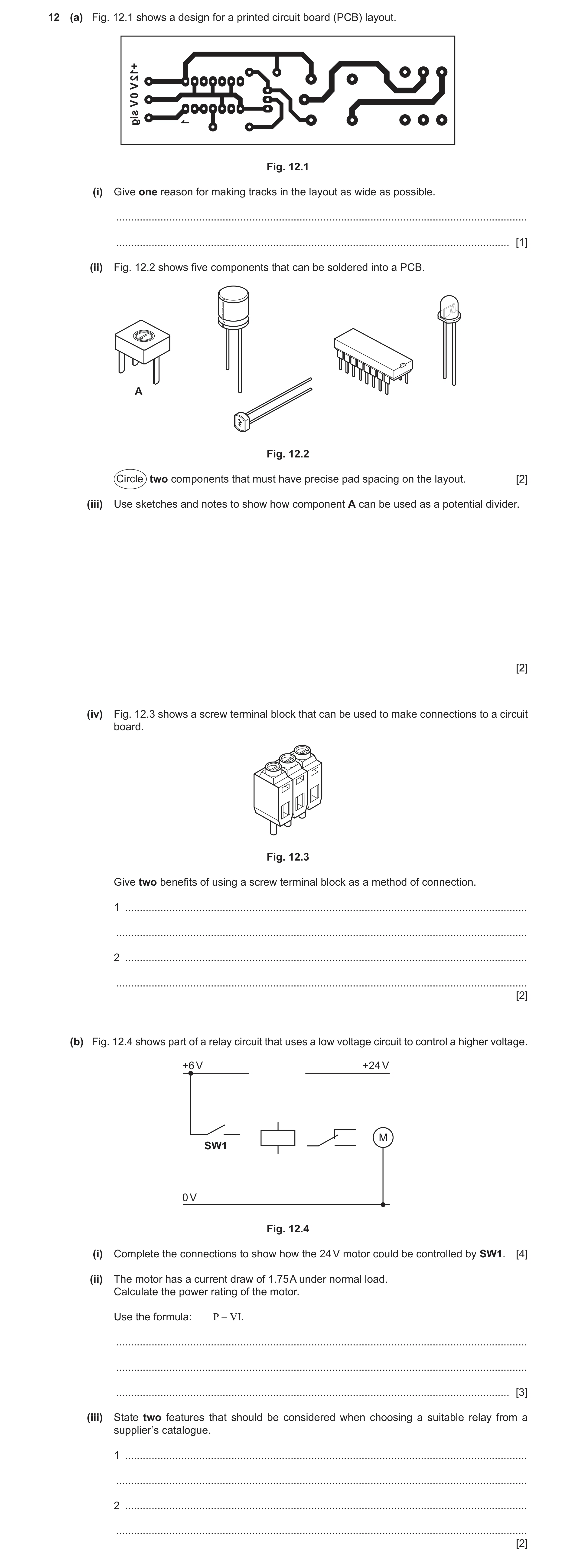
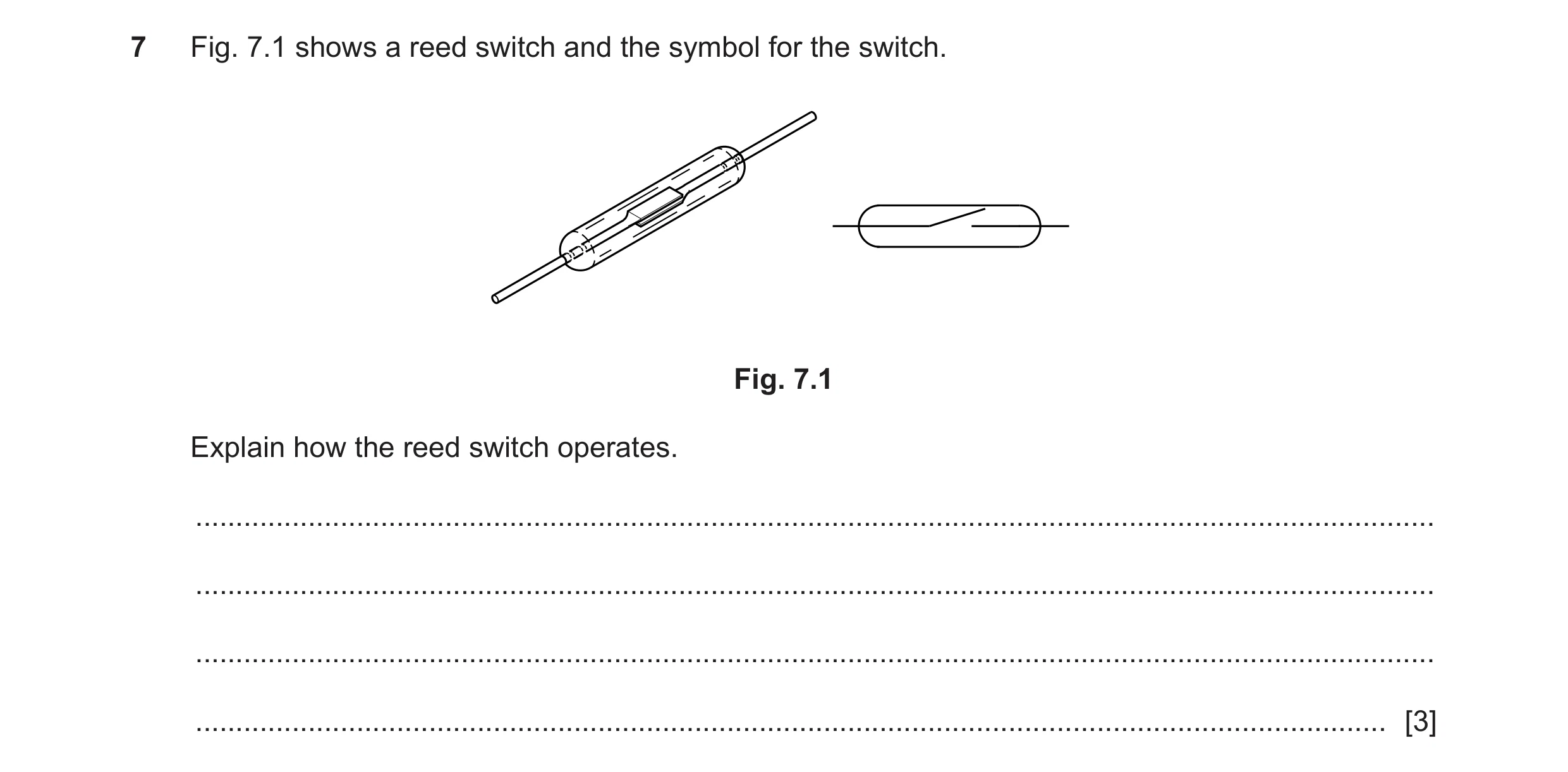 92 / 198
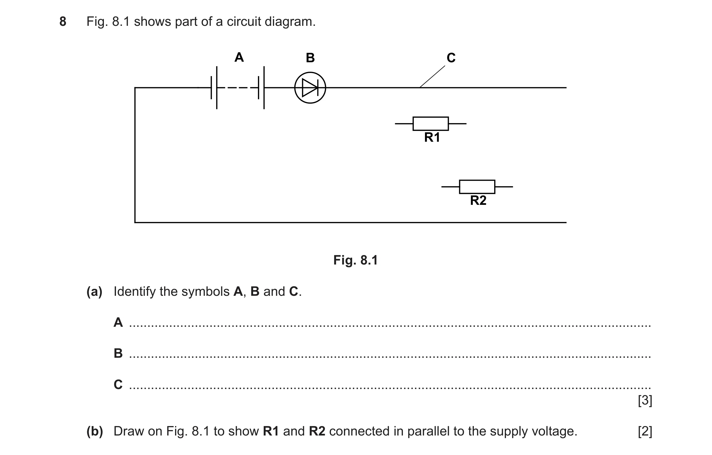 93 / 198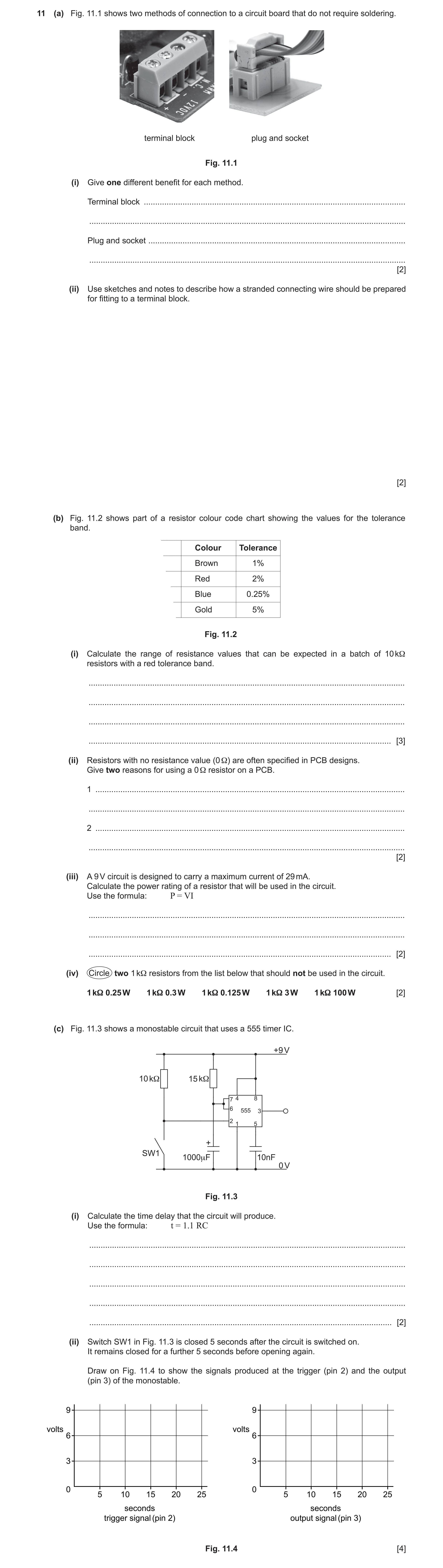
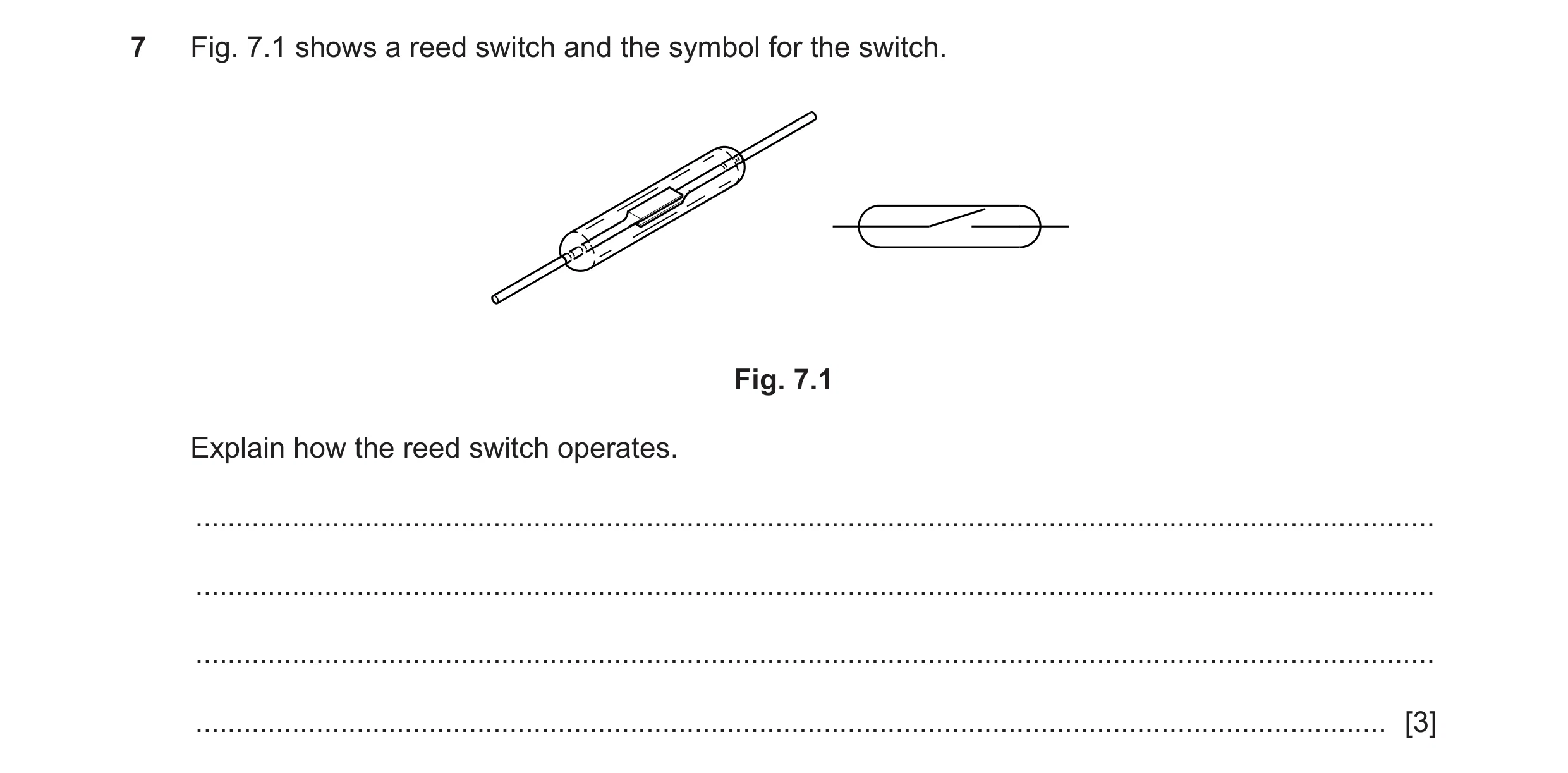 96 / 198
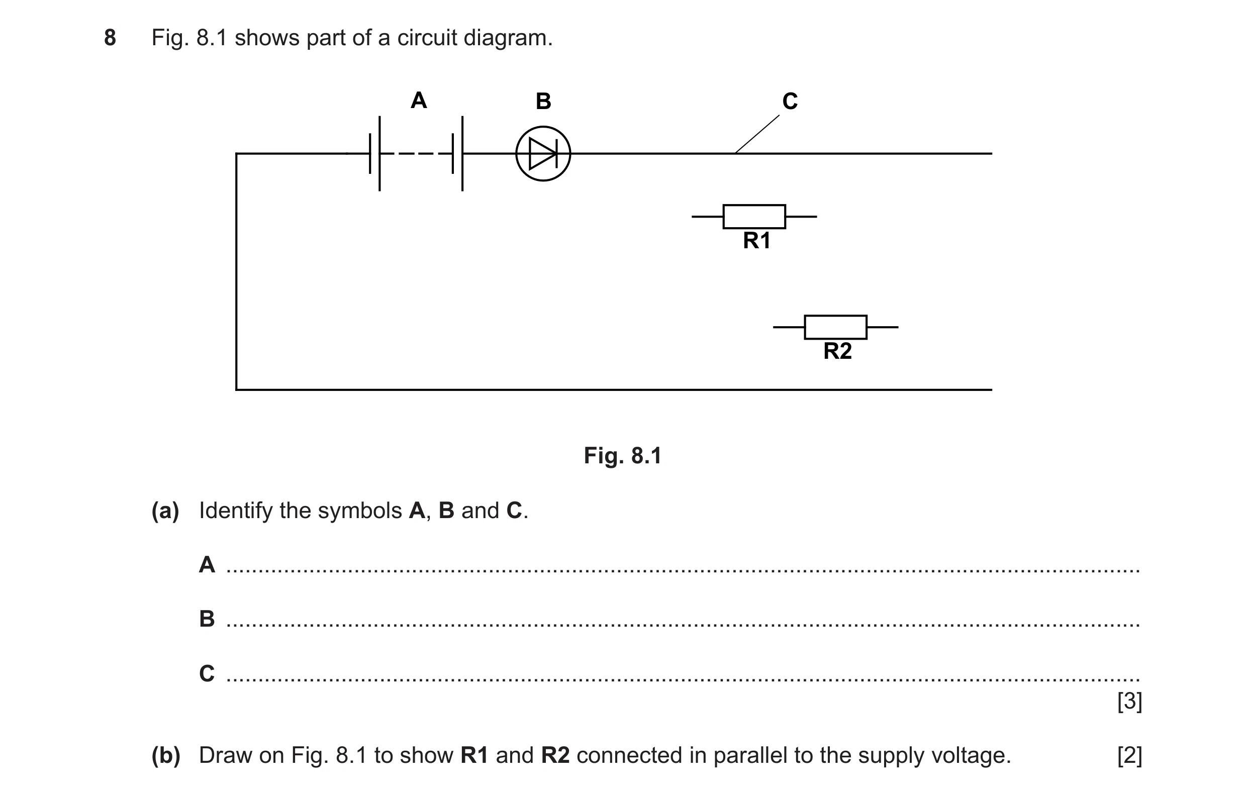 97 / 198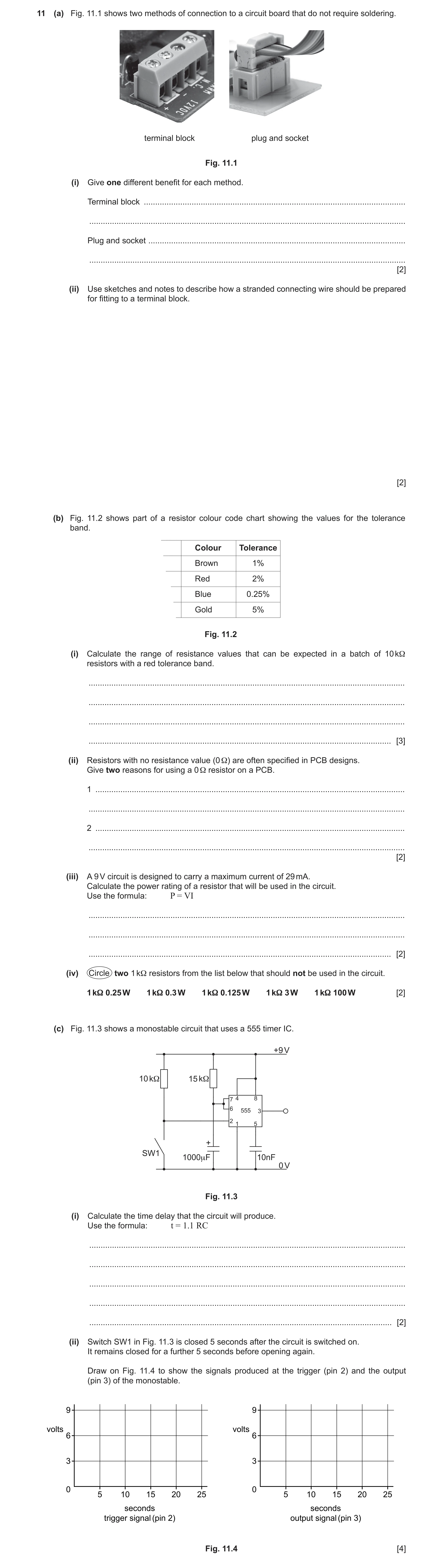
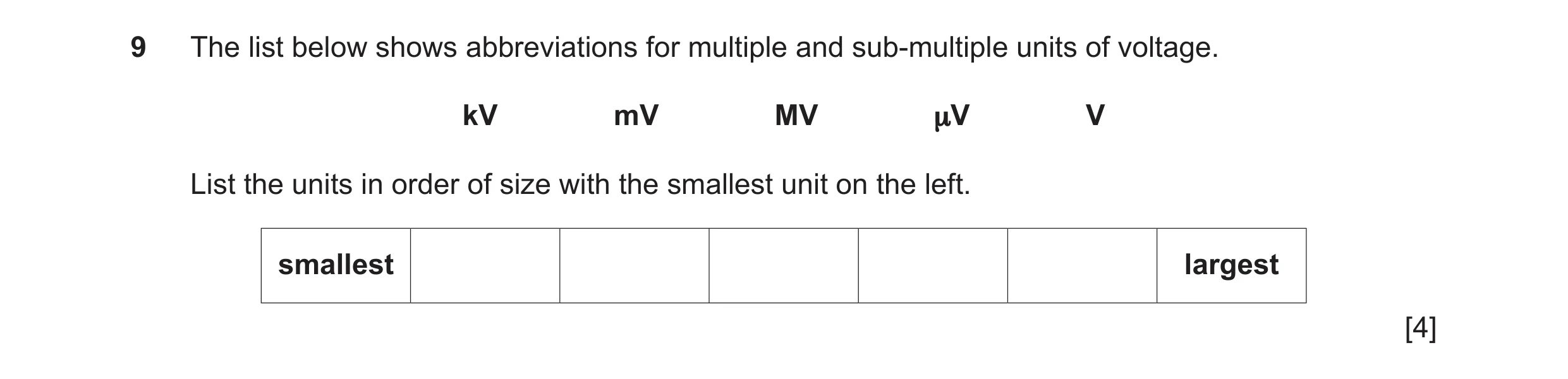 100 / 198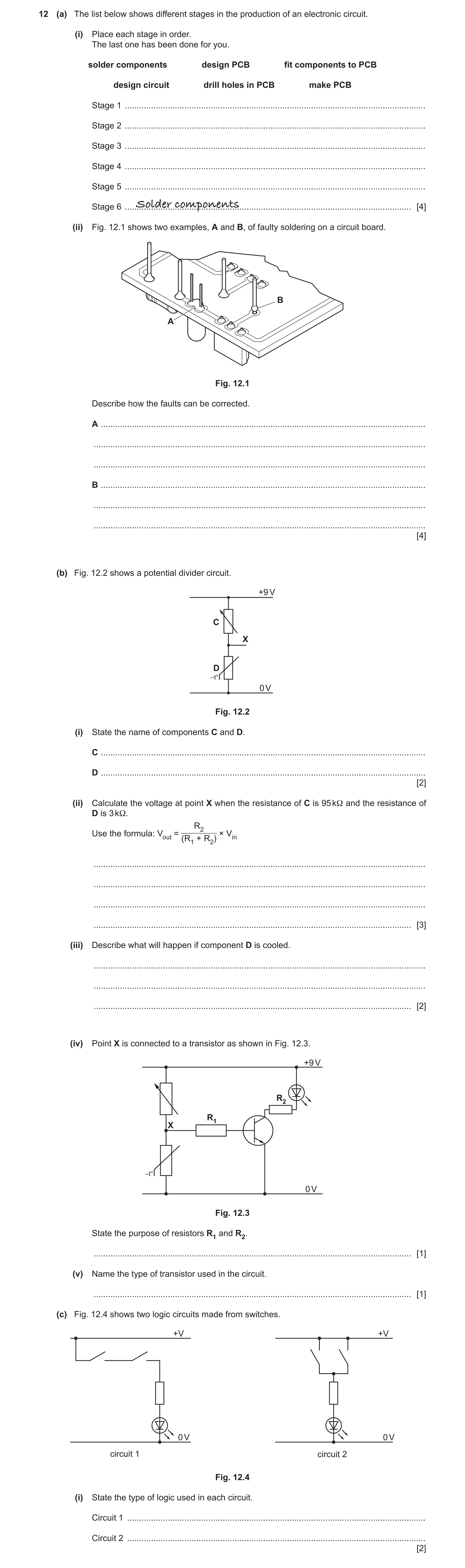
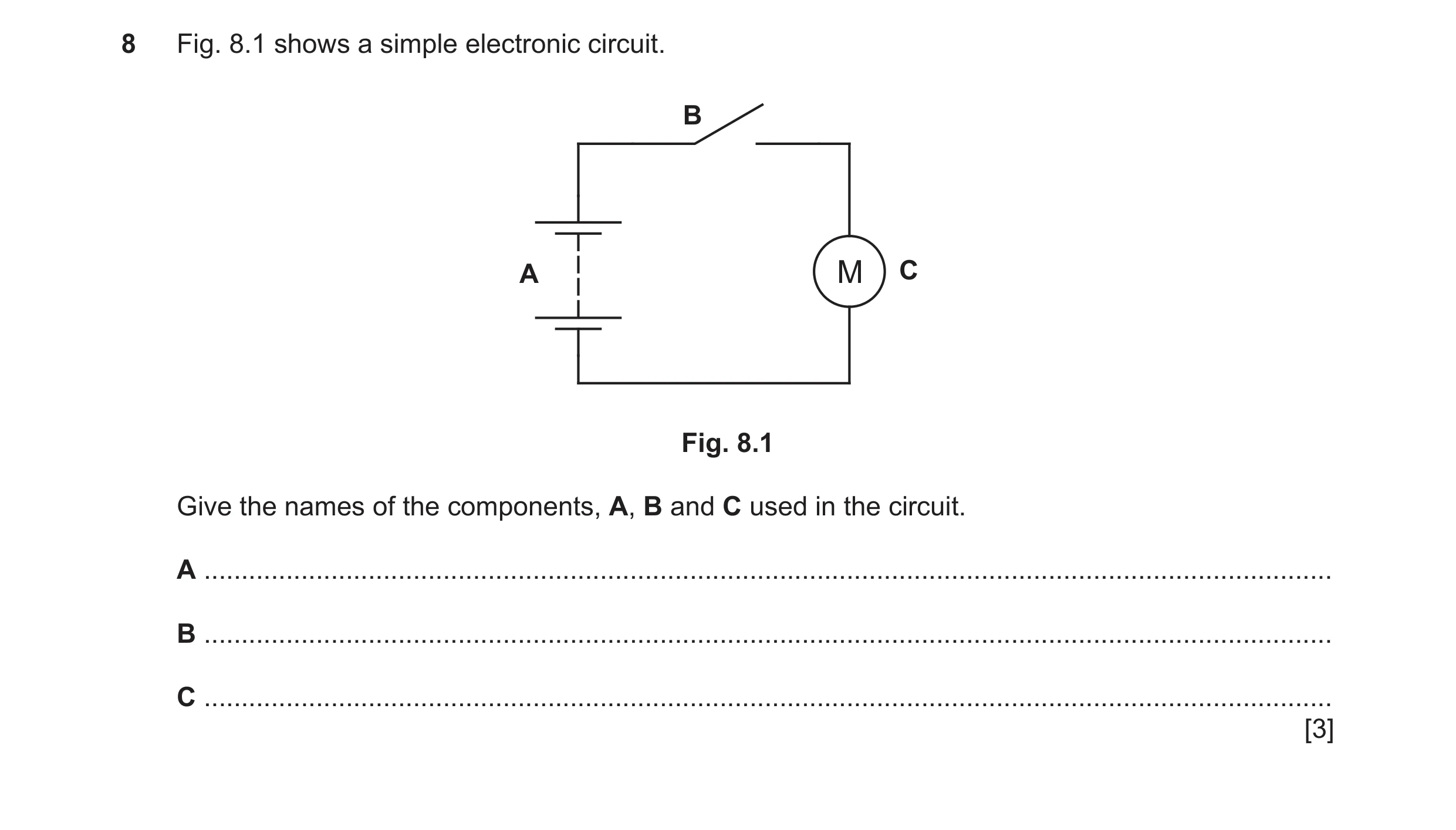
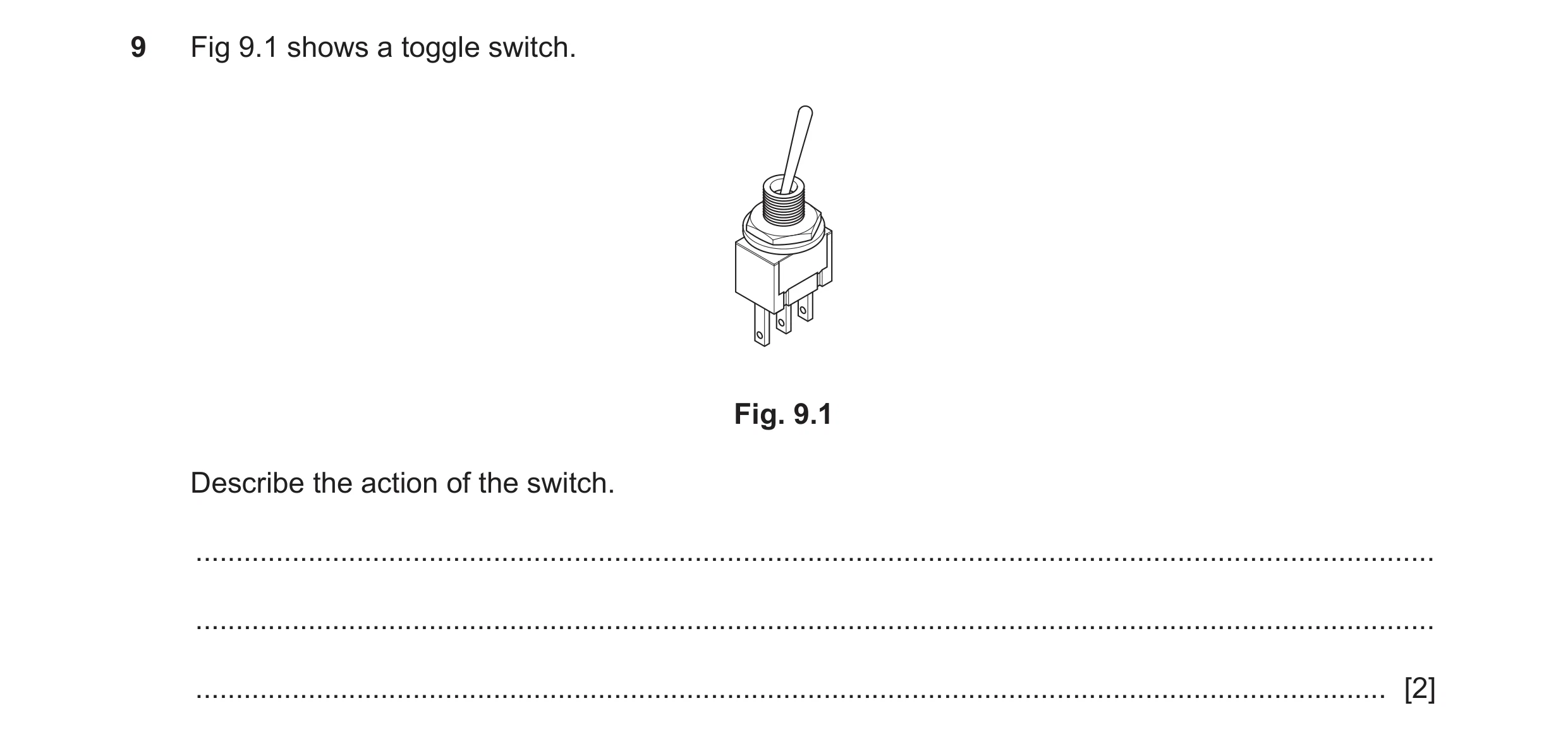 104 / 198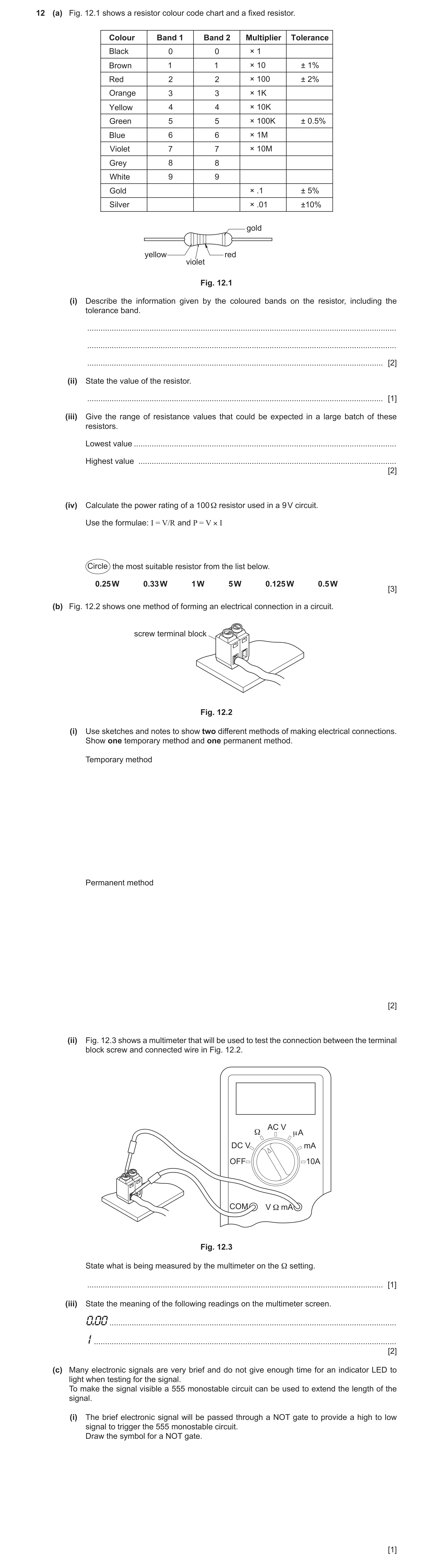
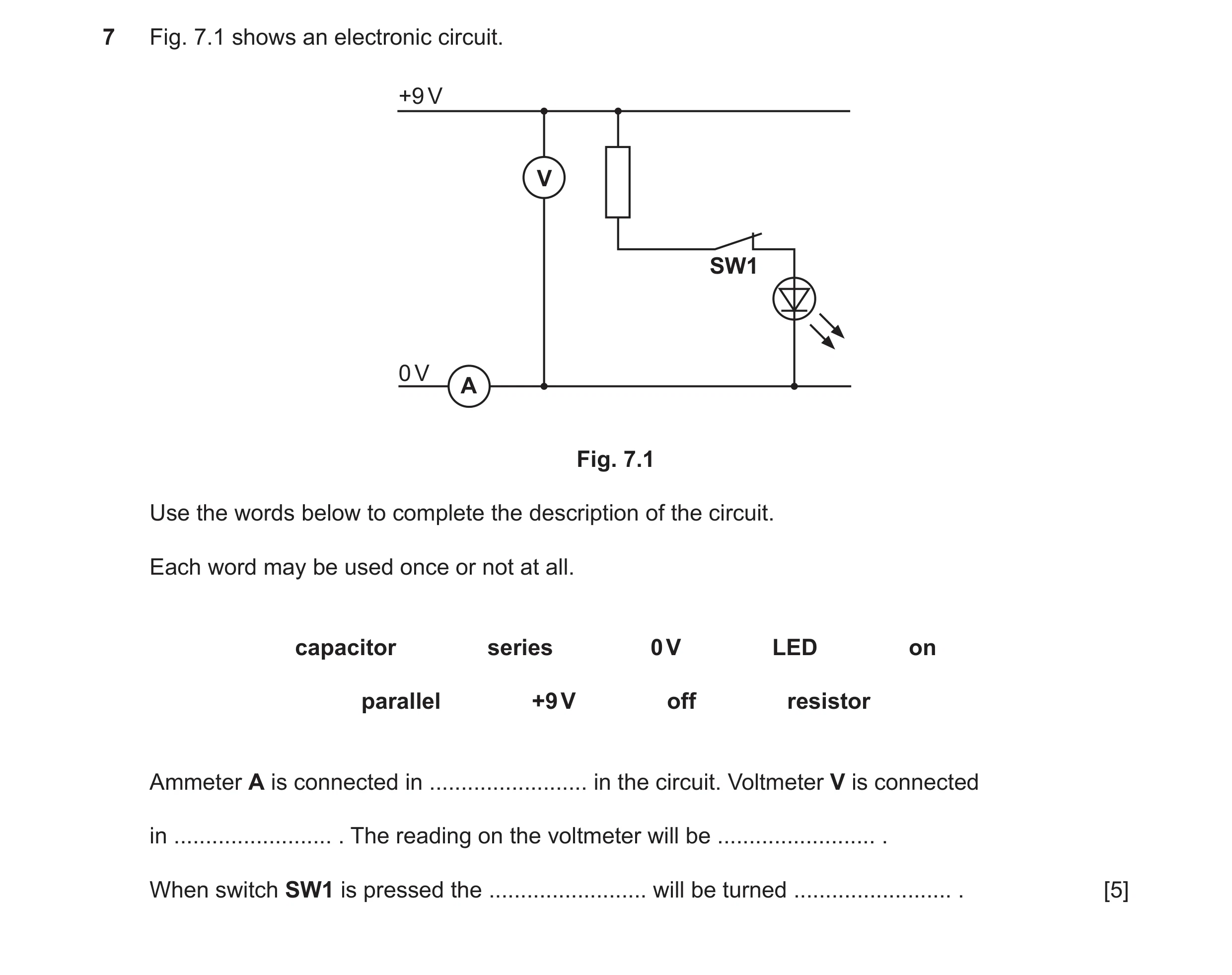
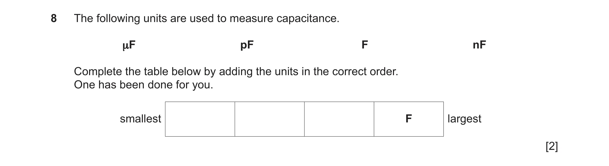 108 / 198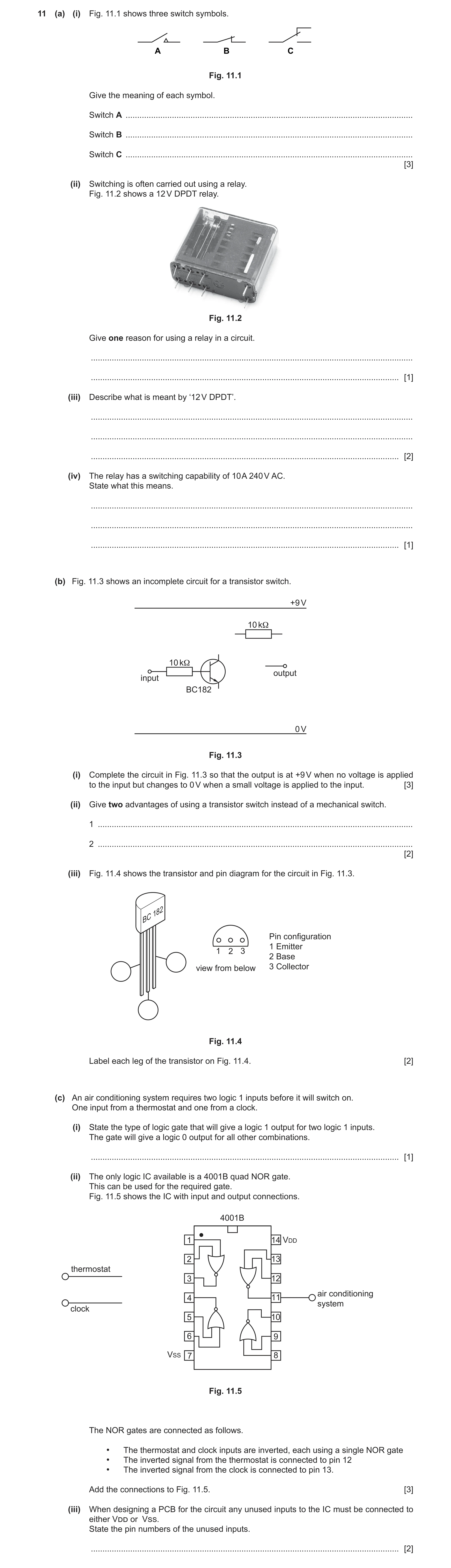
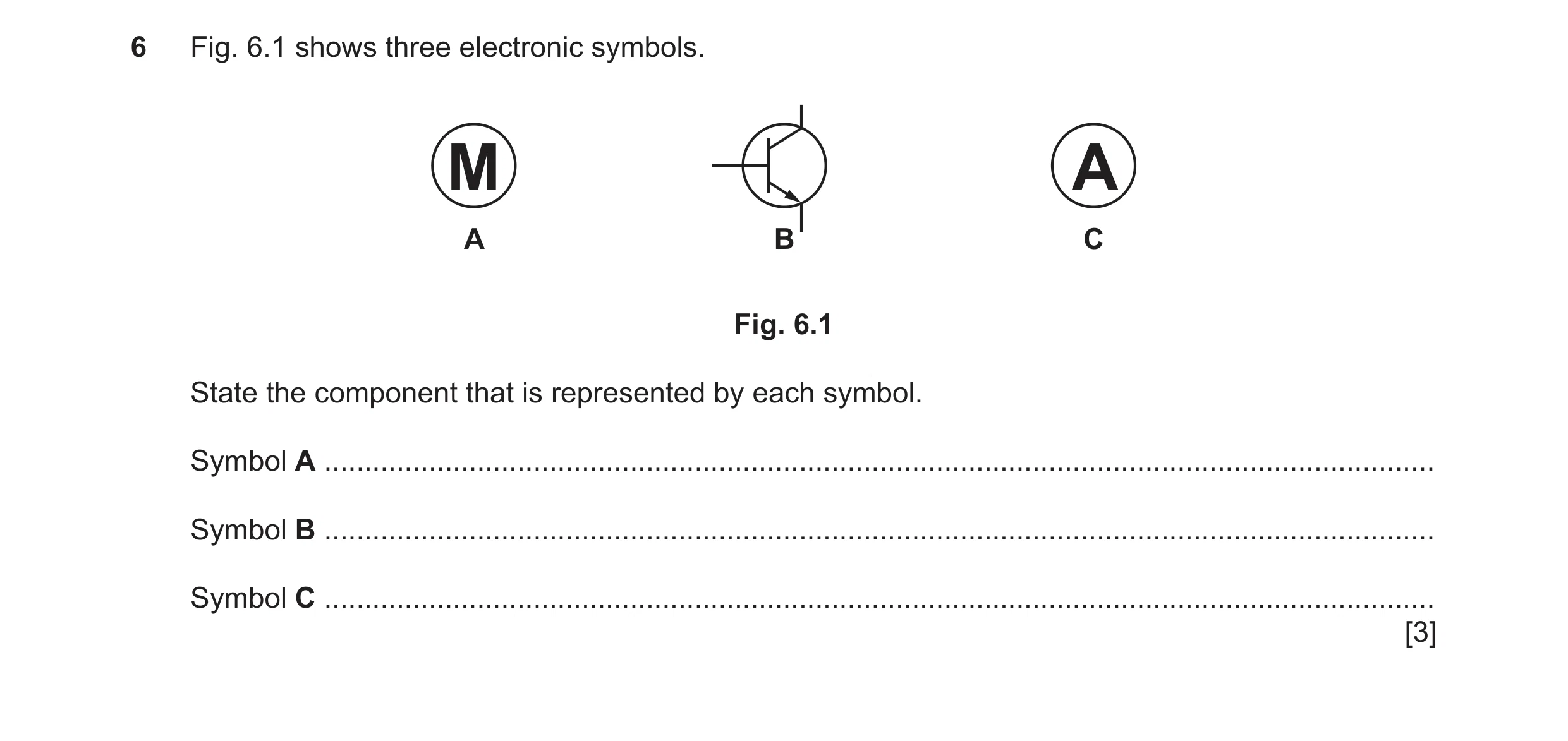

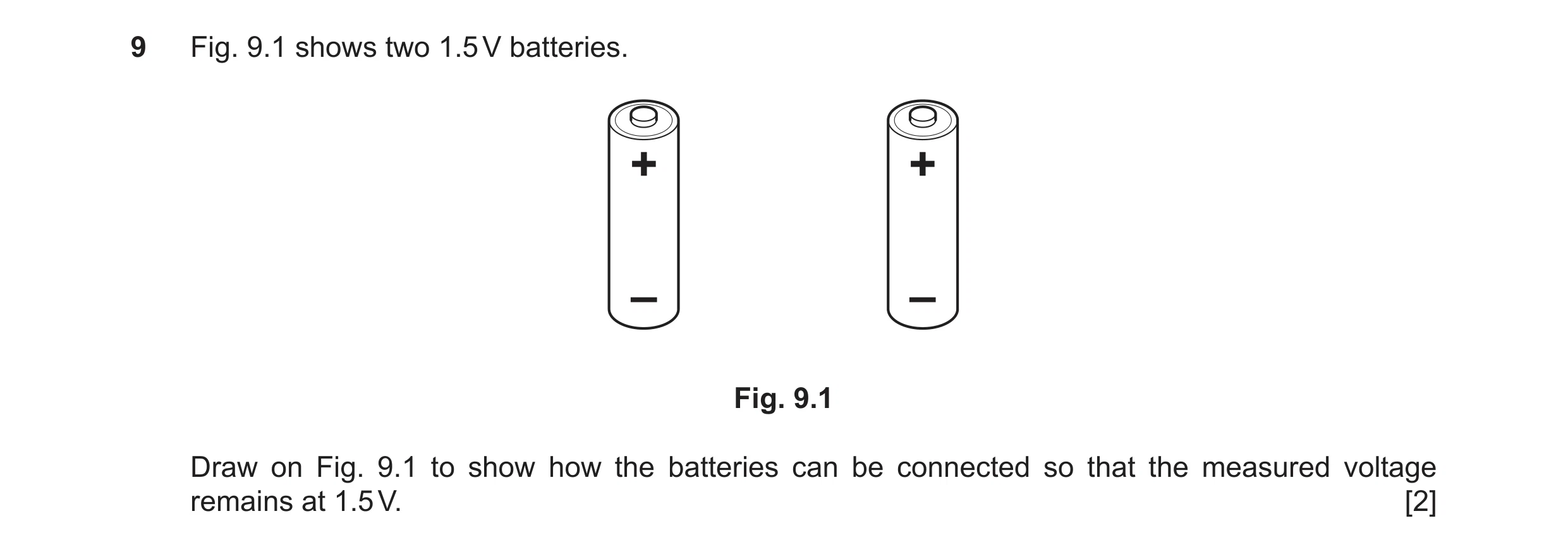 112 / 198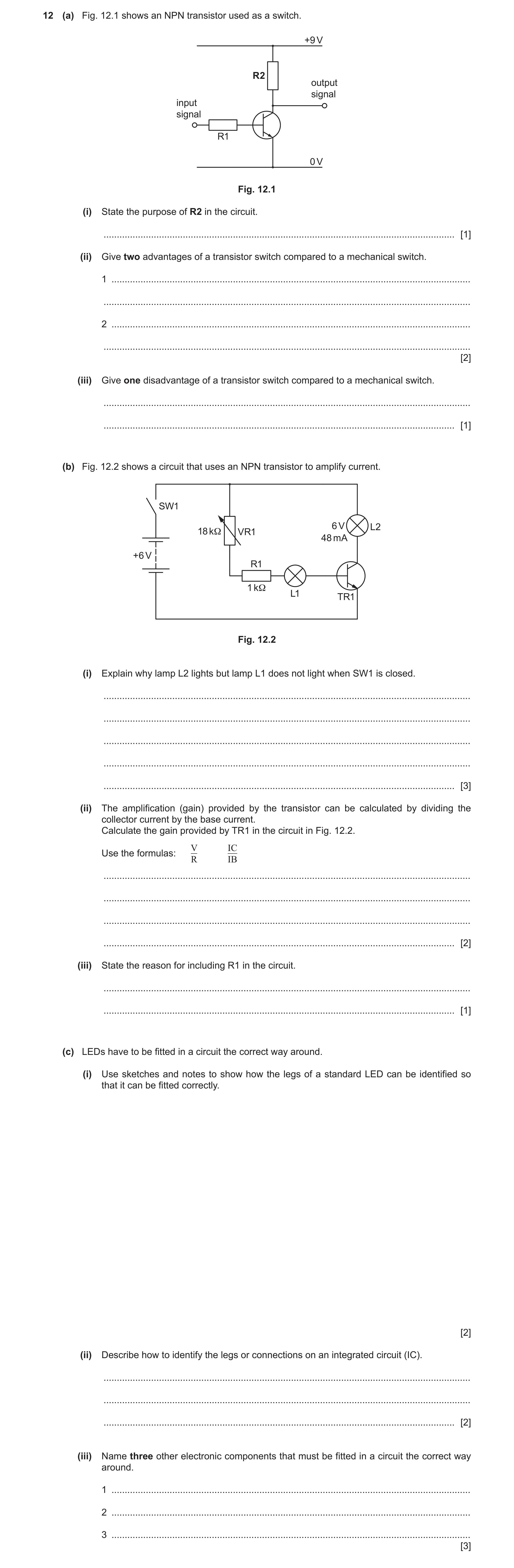

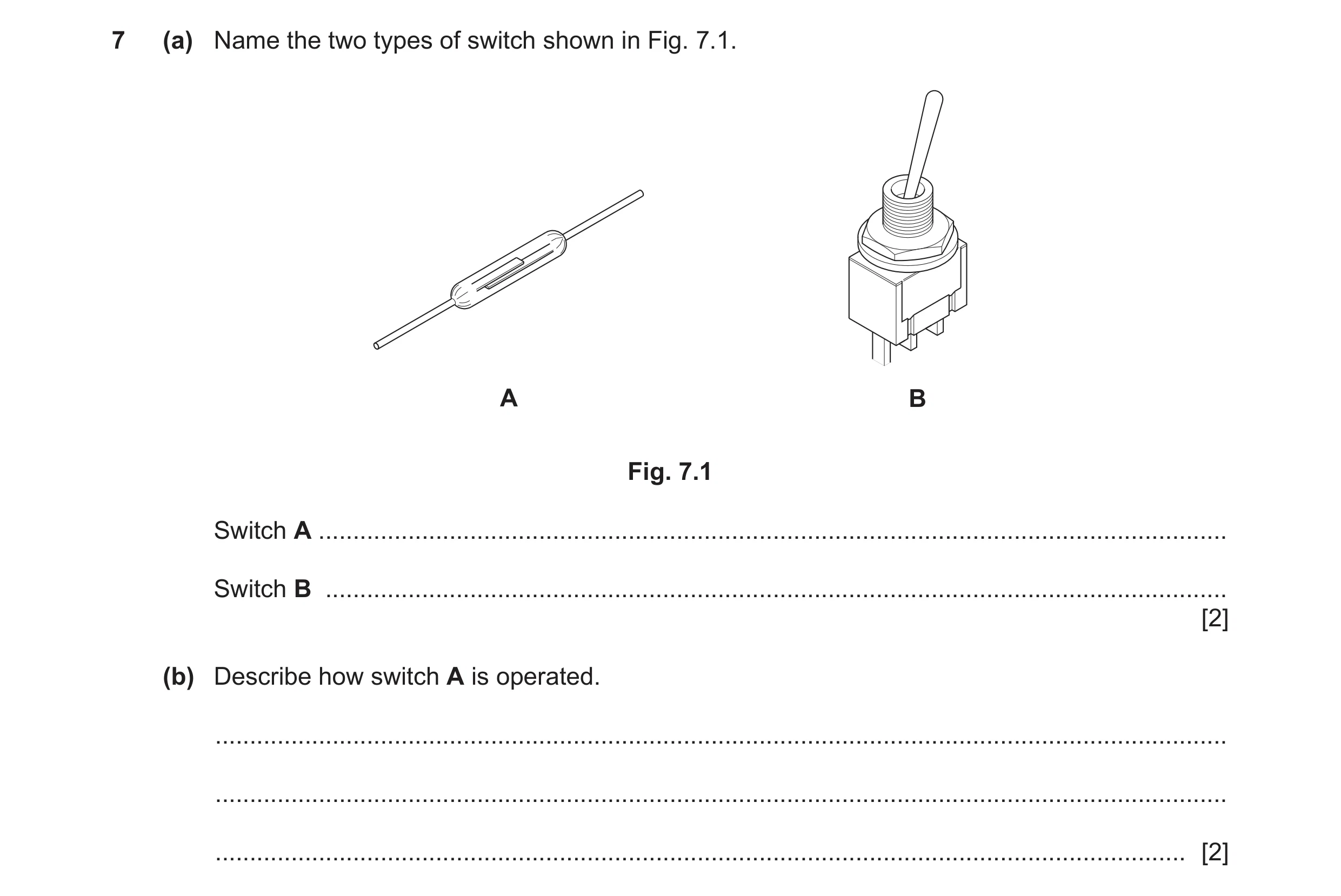 115 / 198
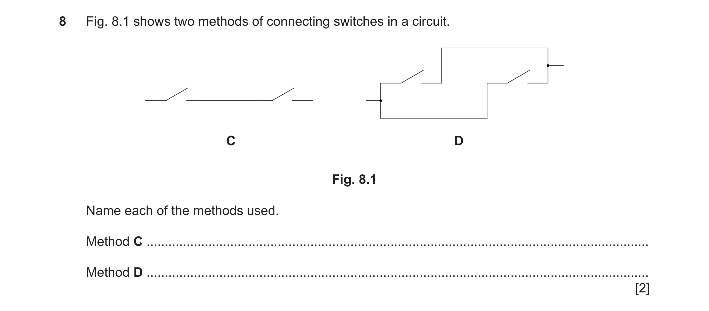 116 / 198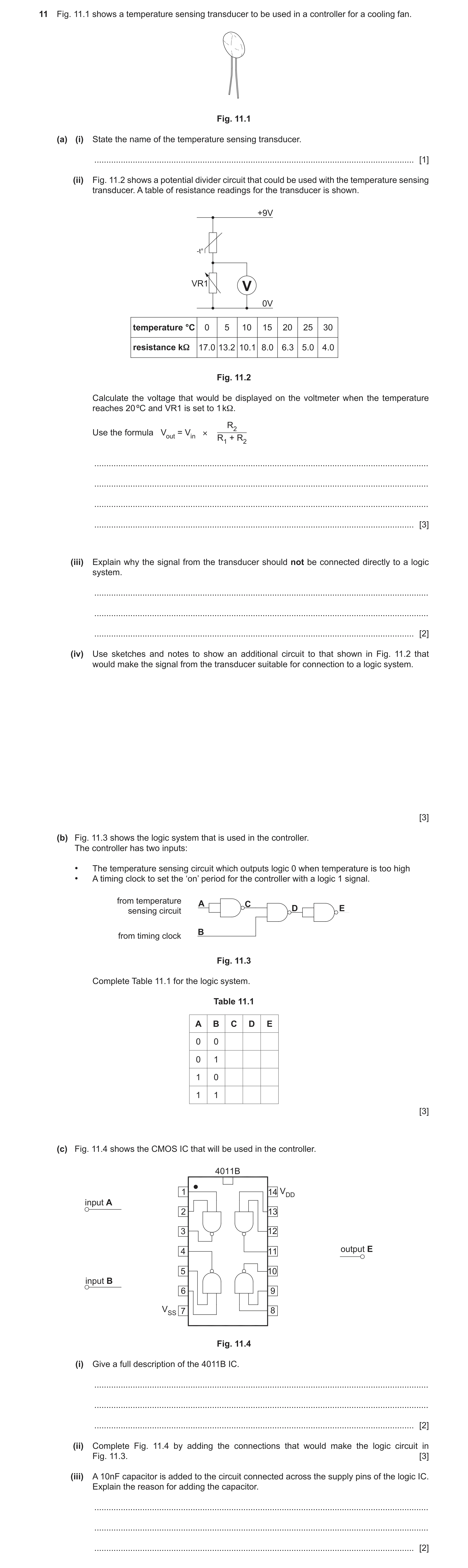
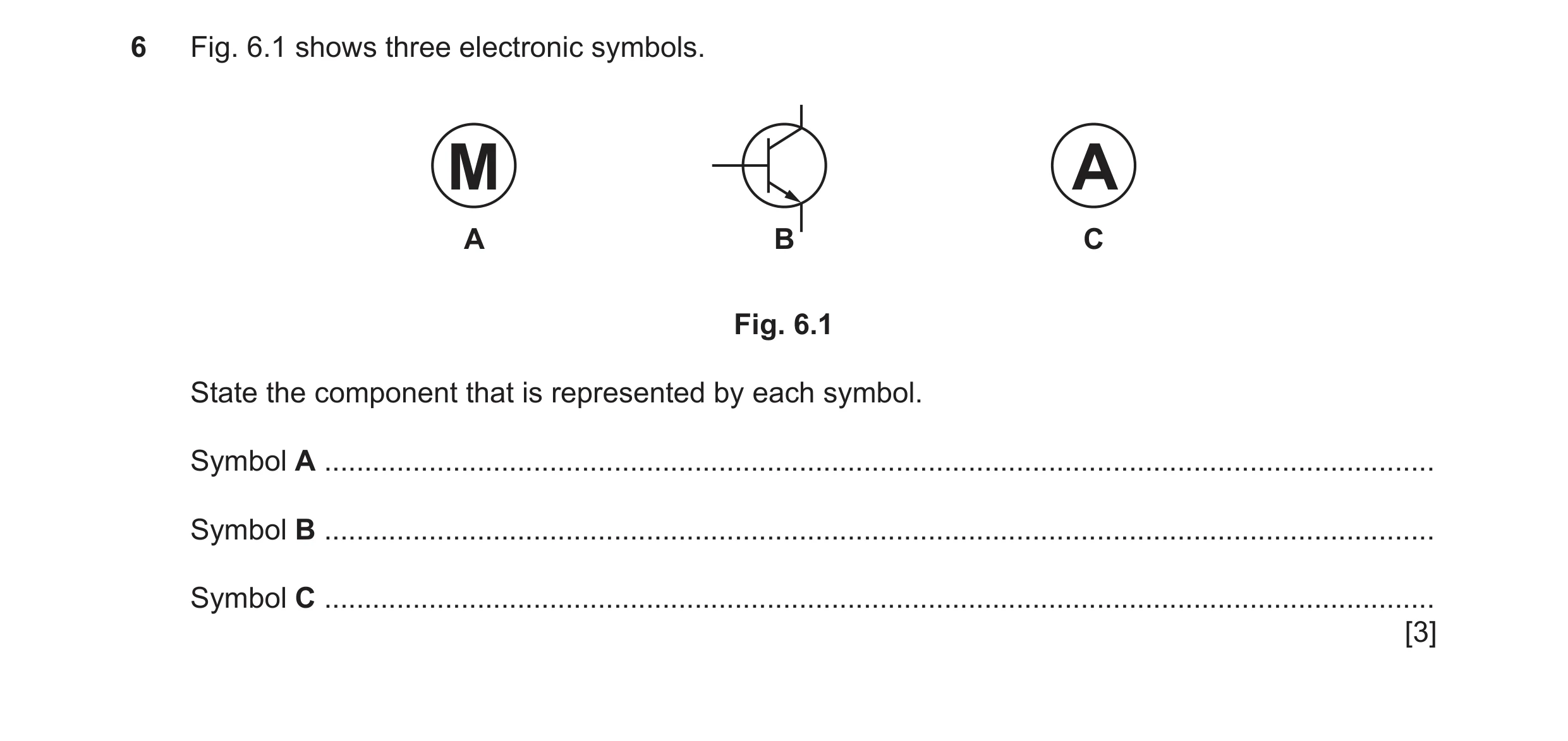 118 / 198

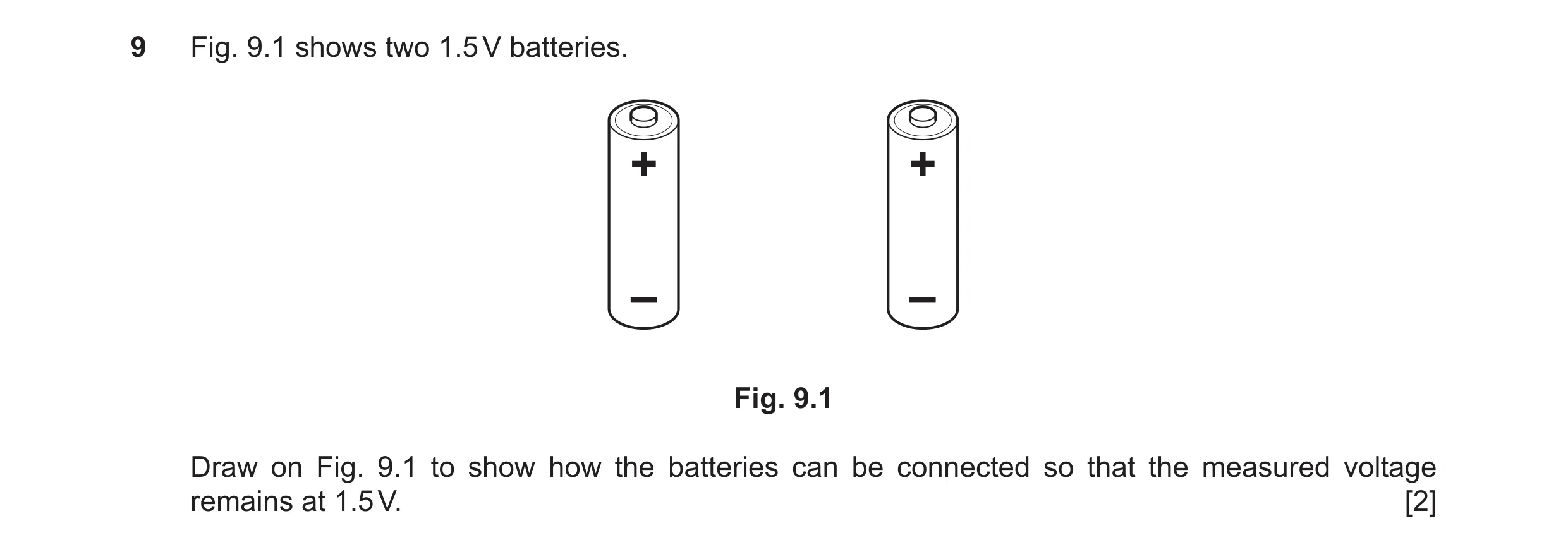 119 / 198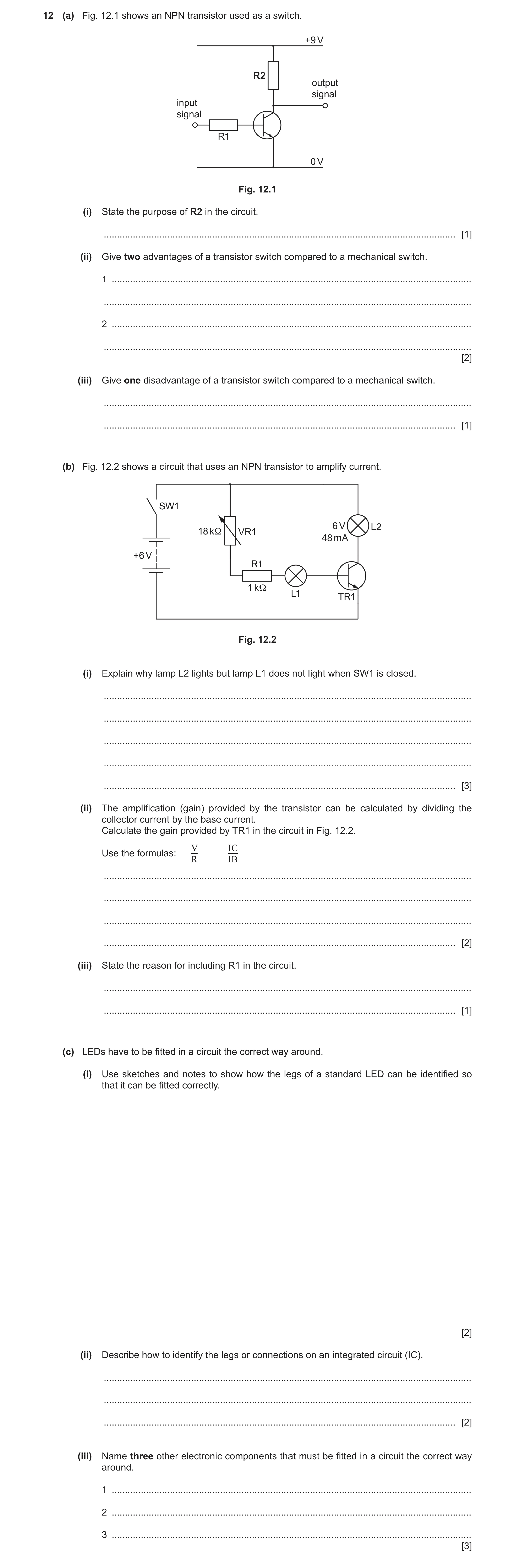
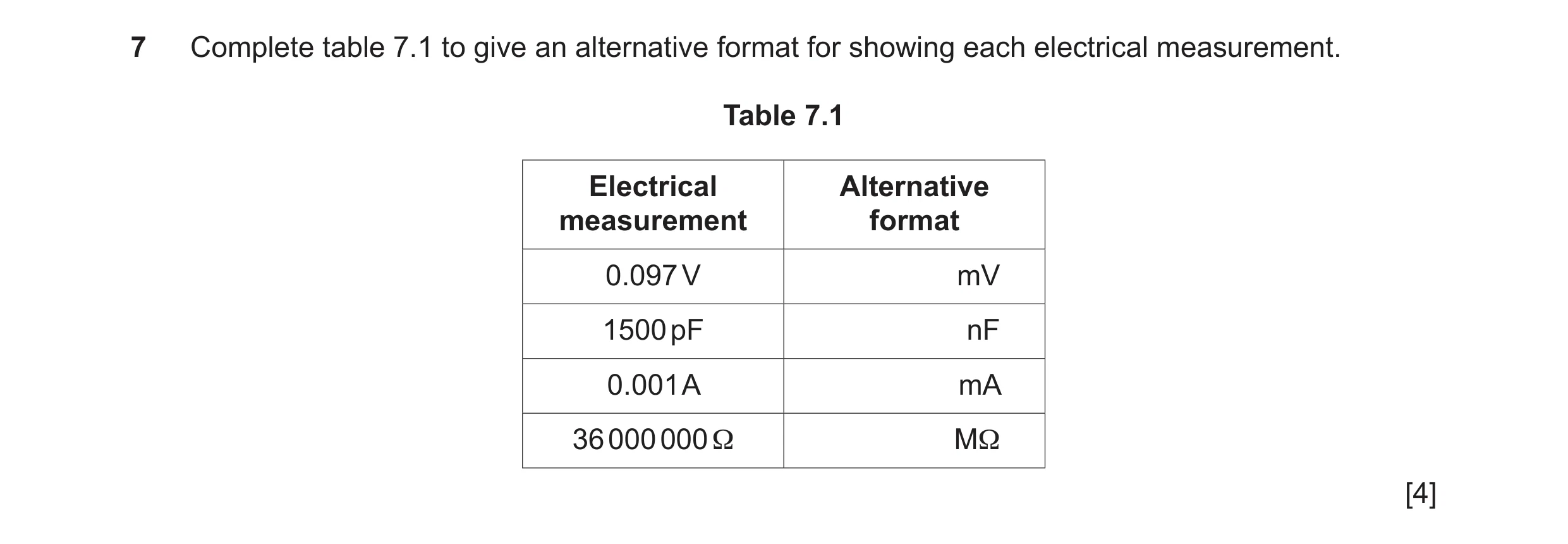 121 / 198
![Question 110: Fig. 8.1 shows a microswitch. NC C NO Fig. 8.1 (a) Draw the circuit symbol for the microswitch. [1] (b) Describe how the microswitch works.…](https://img.pastlit.com/crops/e216b99e-c2f8-4f27-ac4f-dc25f901b752/q8.webp)
 122 / 198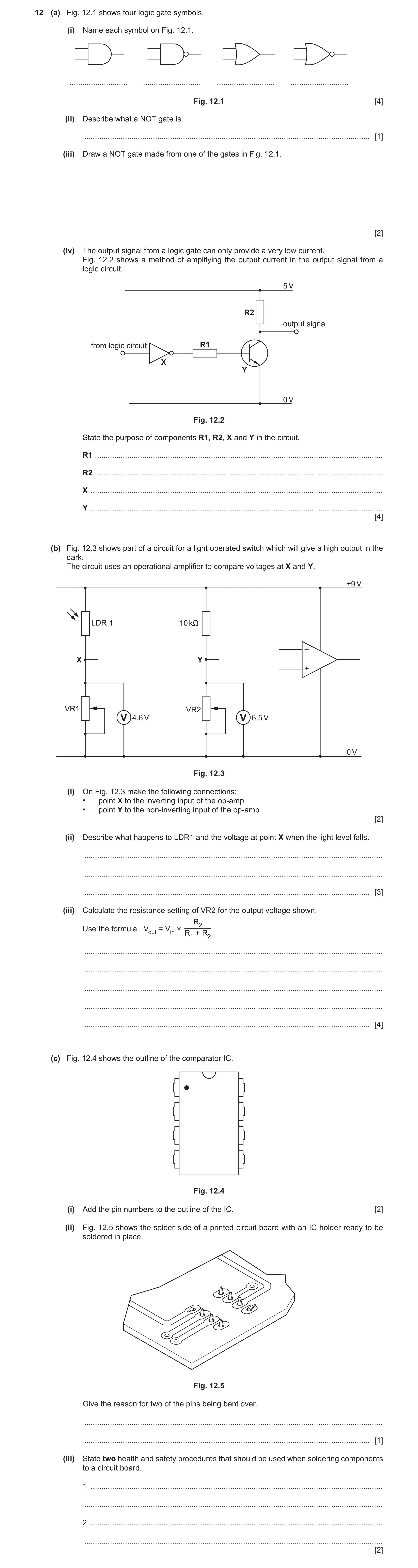
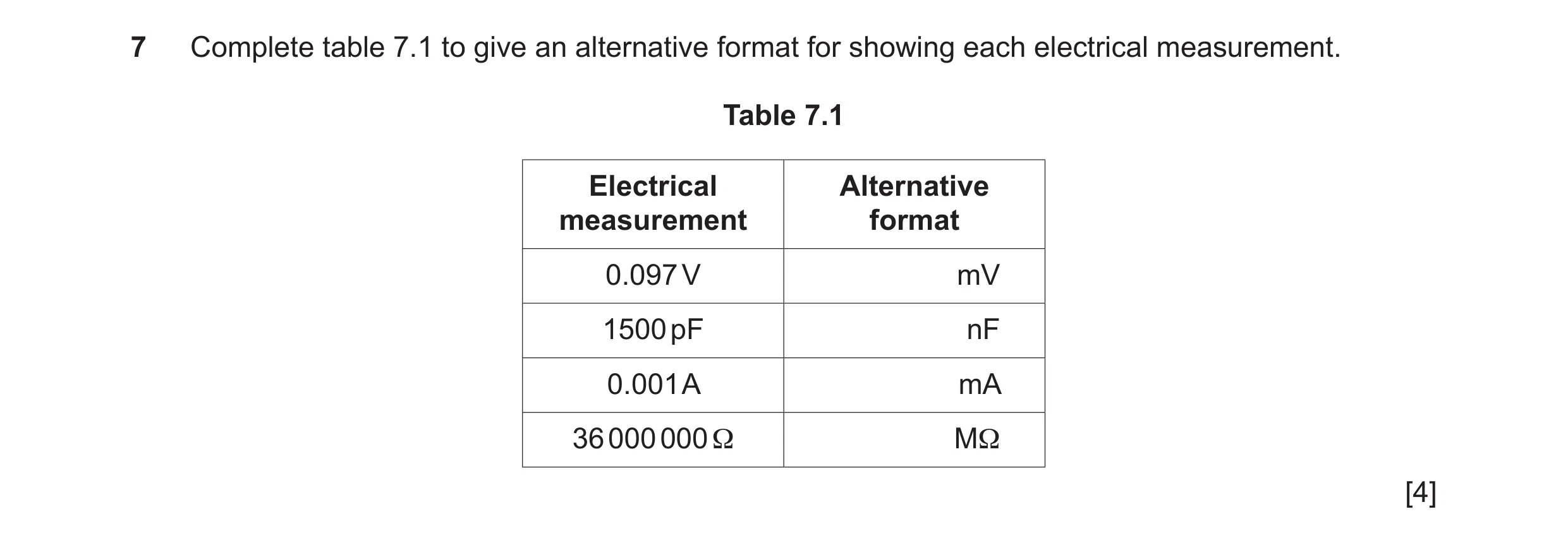
![Question 114: Fig. 8.1 shows a microswitch. NC C NO Fig. 8.1 (a) Draw the circuit symbol for the microswitch. [1] (b) Describe how the microswitch works.…](https://img.pastlit.com/crops/281bfa56-352e-45b0-9d16-96f87398aead/q8.webp) 126 / 198
126 / 198 127 / 198
 131 / 198
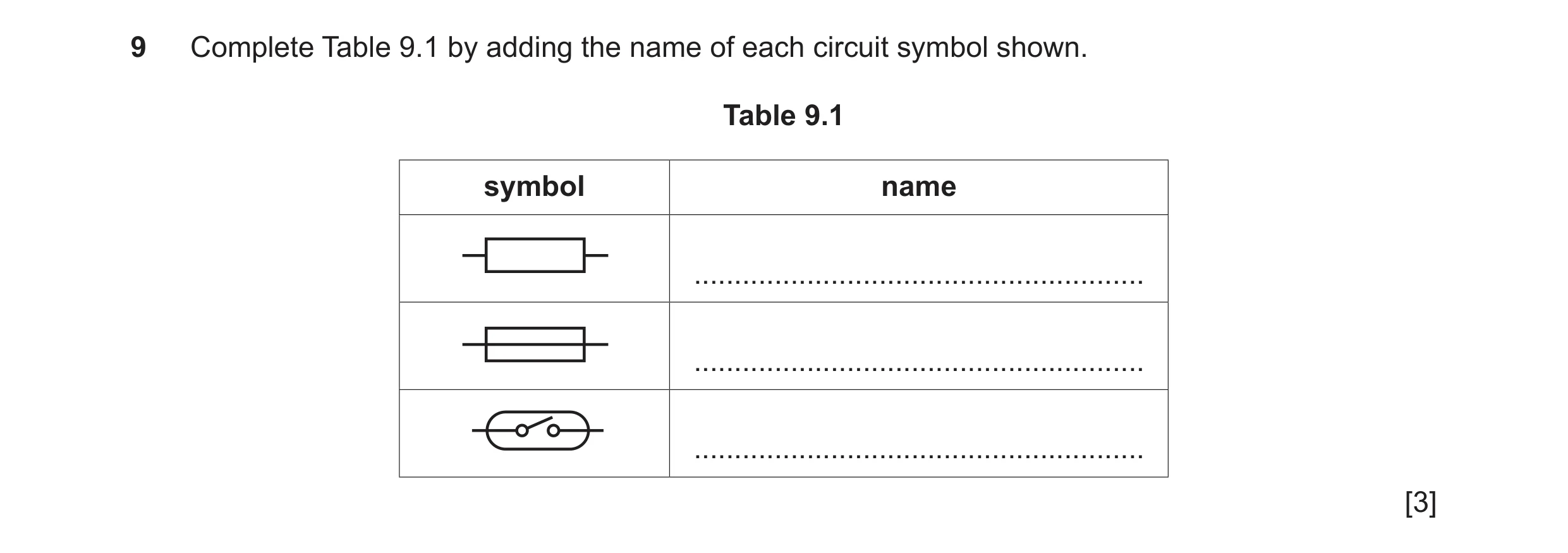 132 / 198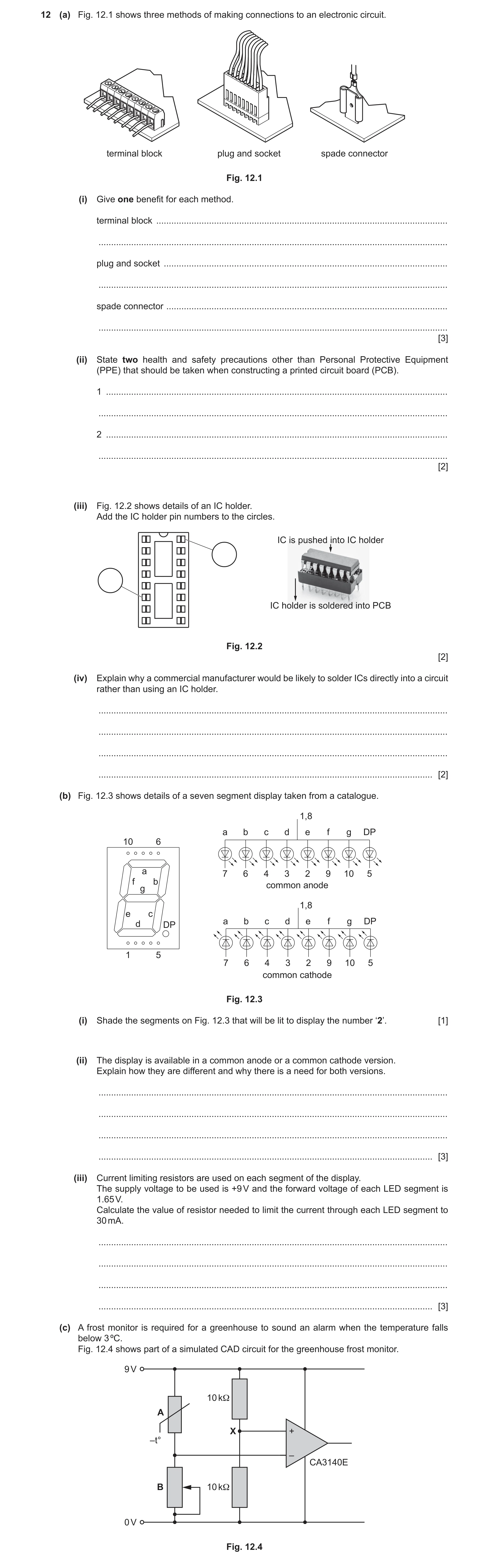
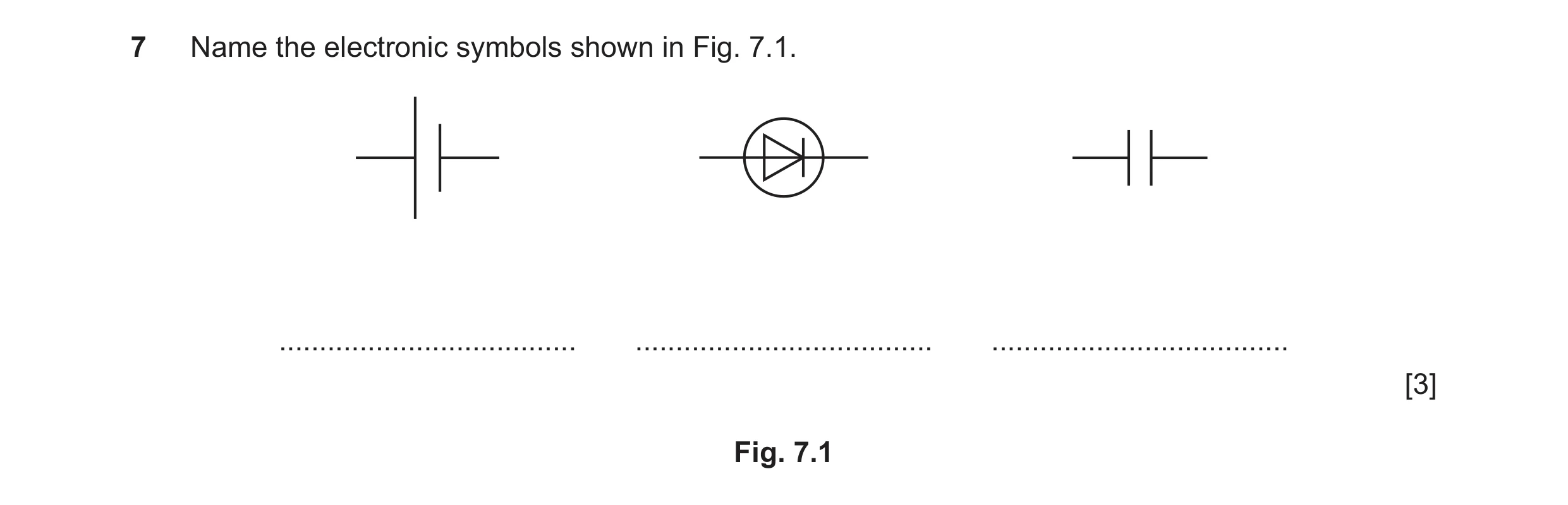 134 / 198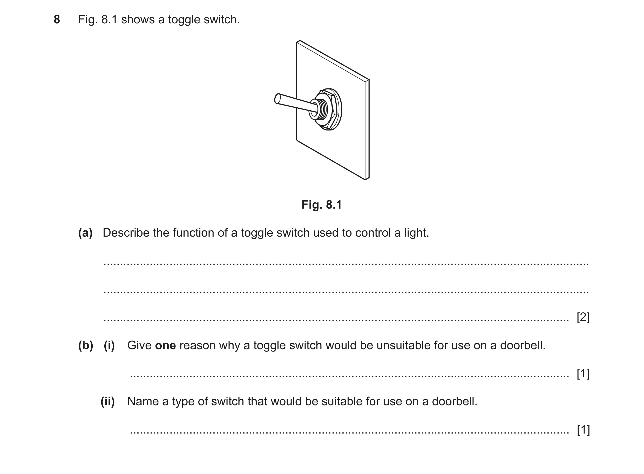
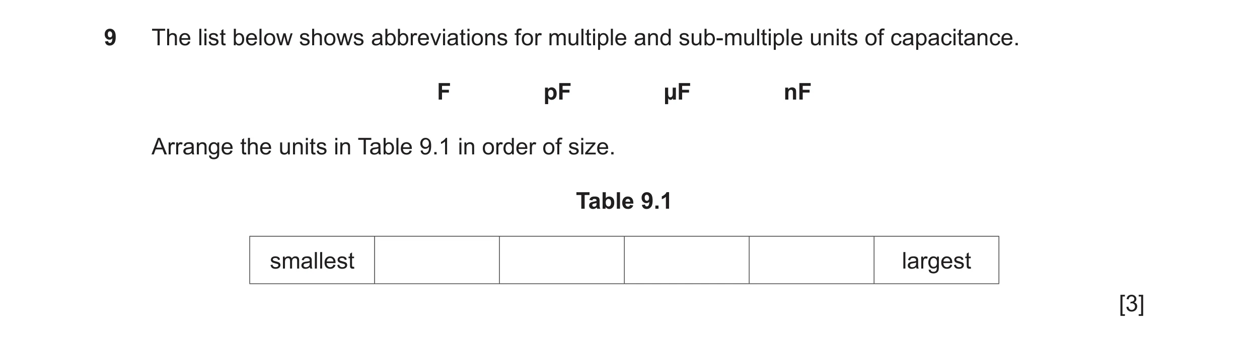 135 / 198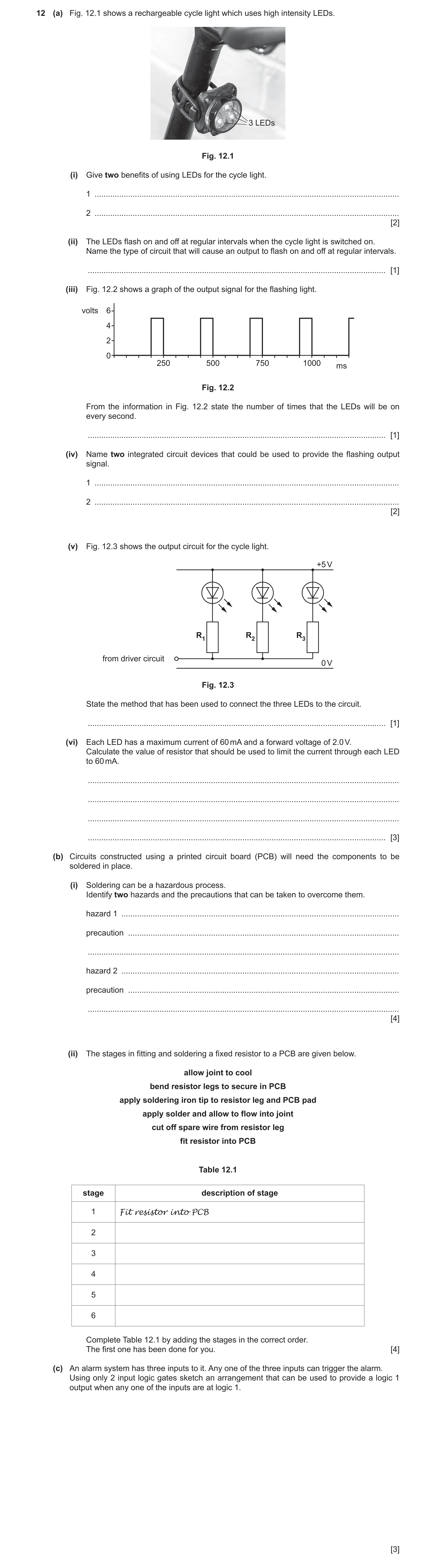
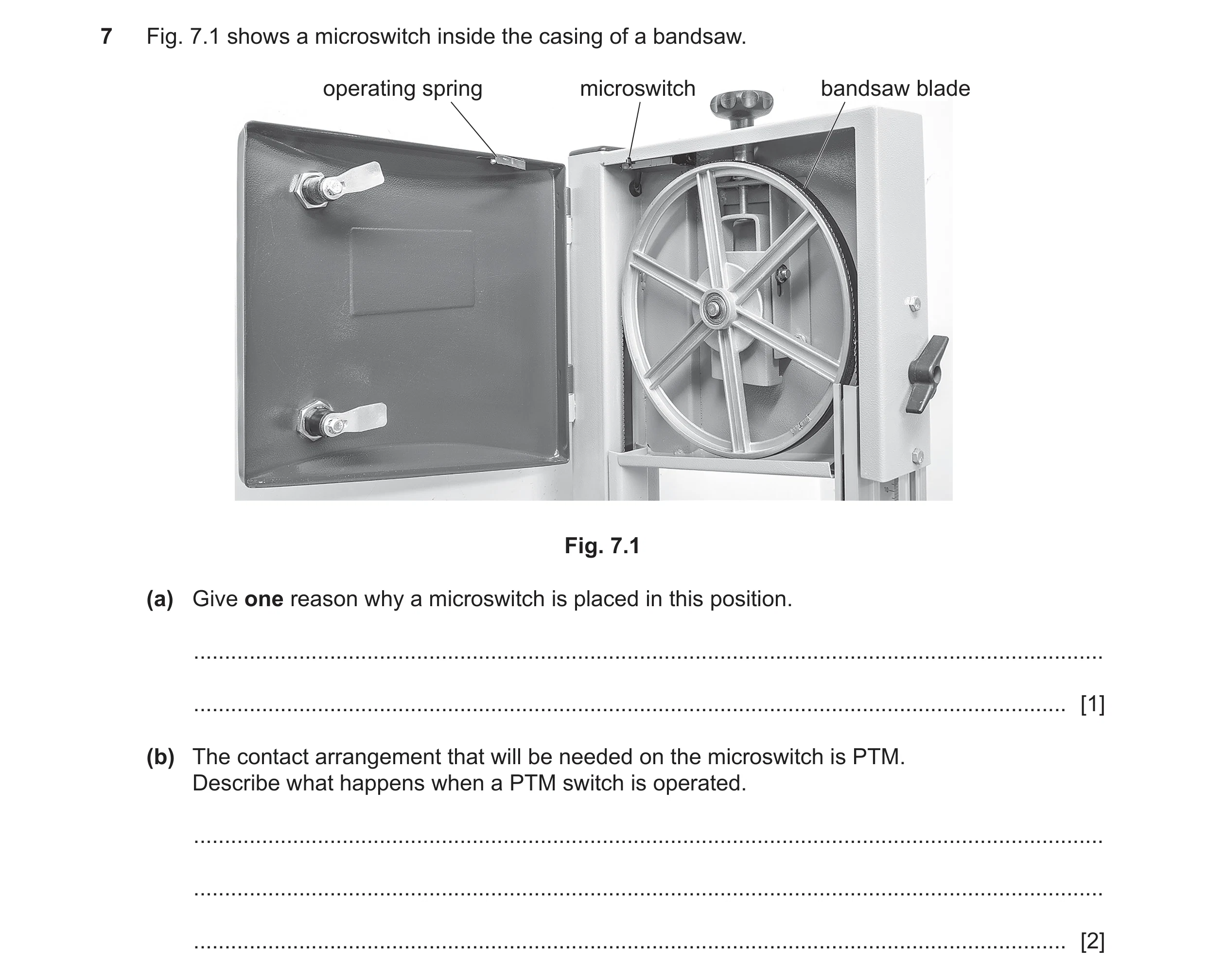
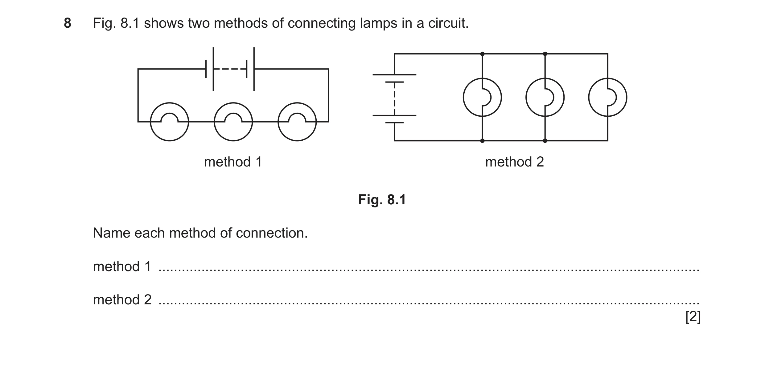 139 / 198
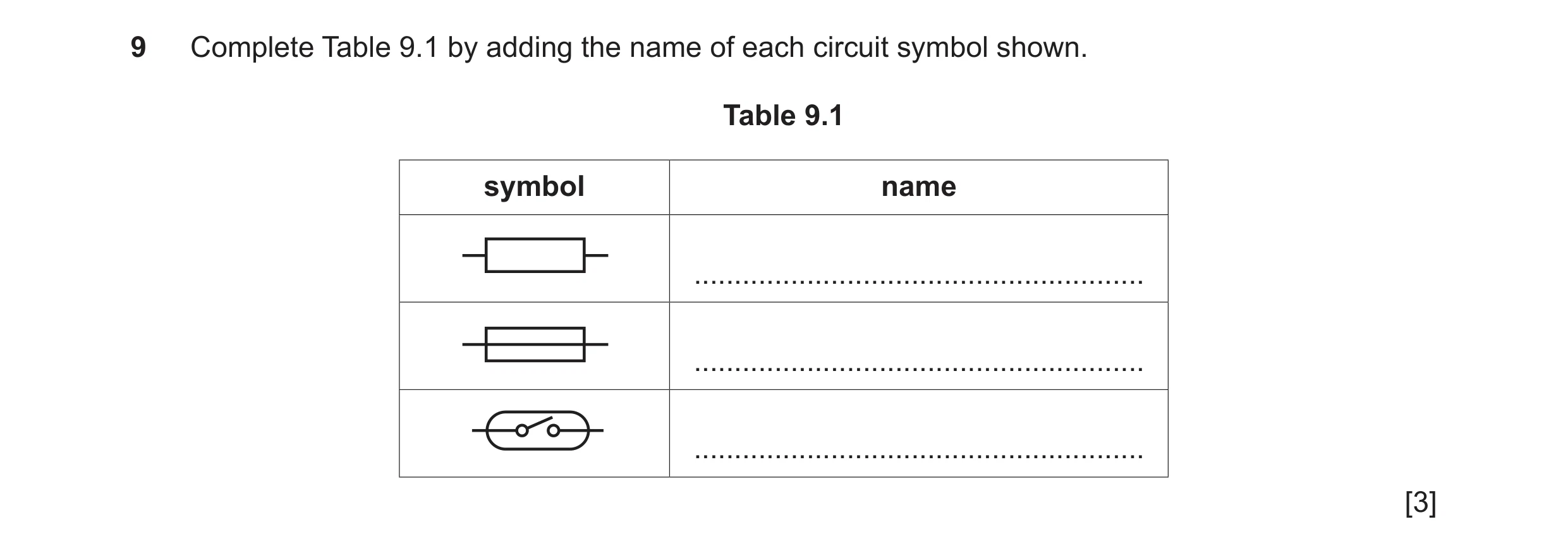 140 / 198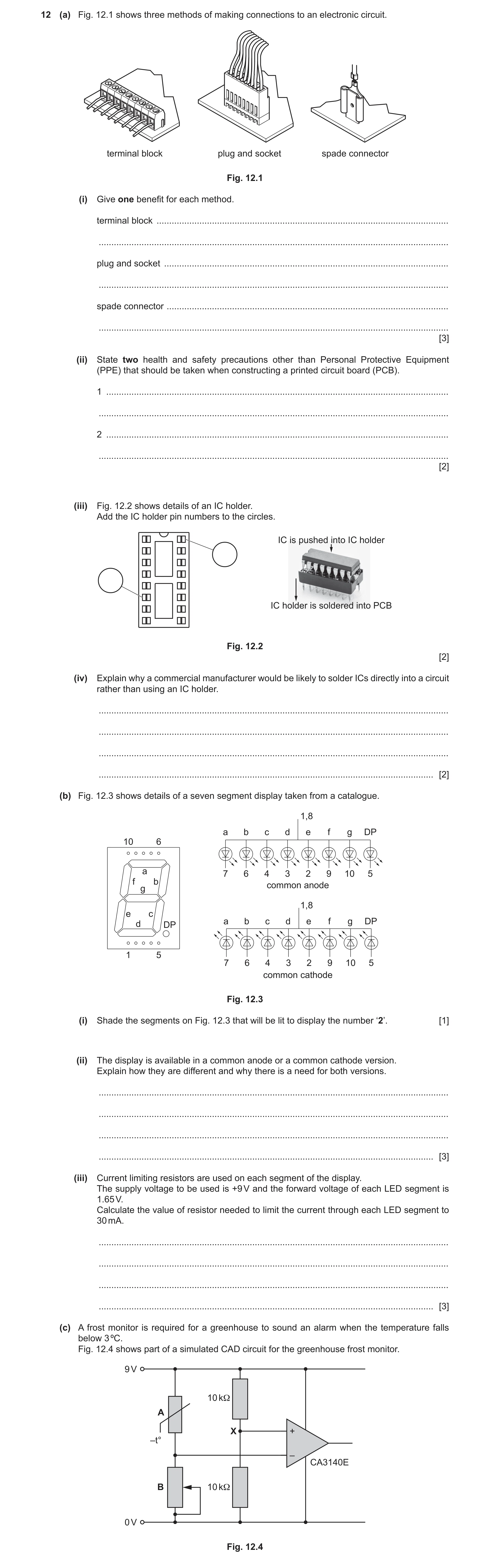
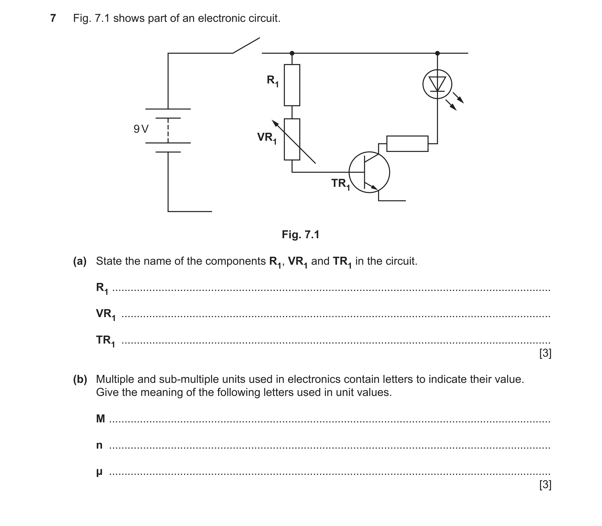
![Question 130: Use sketches and notes to describe how a reed switch is operated. [2]](https://img.pastlit.com/crops/4d698de2-90d7-4441-ad92-56f7a9adeddb/q8.webp) 143 / 198
143 / 198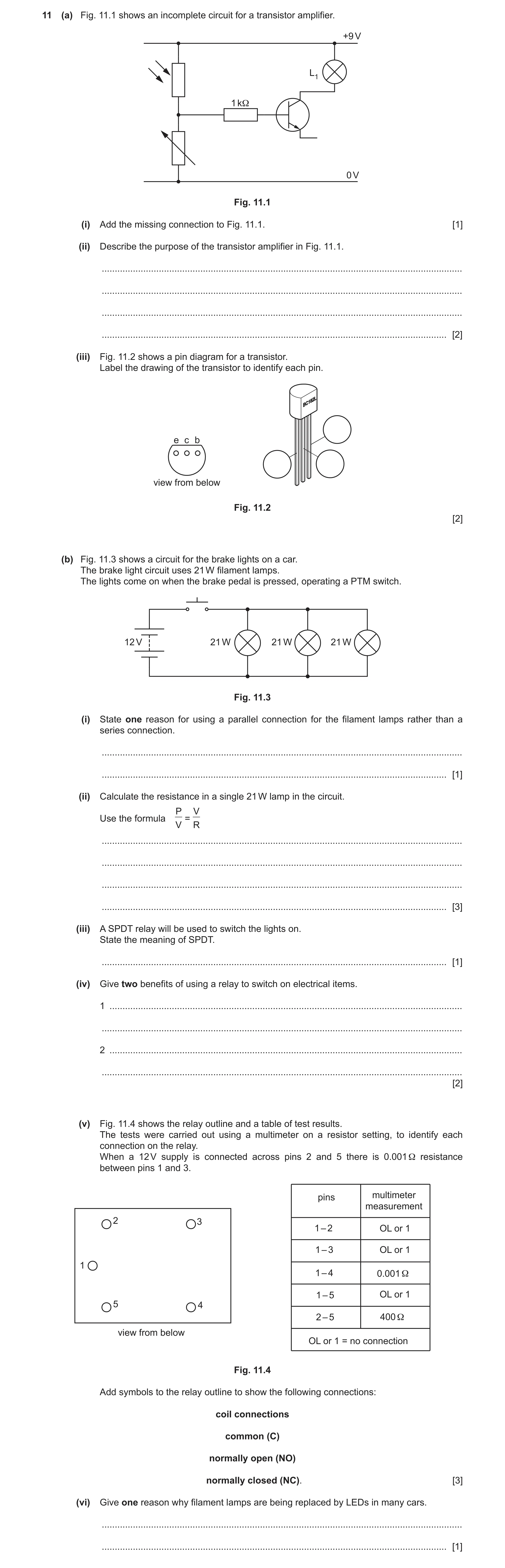
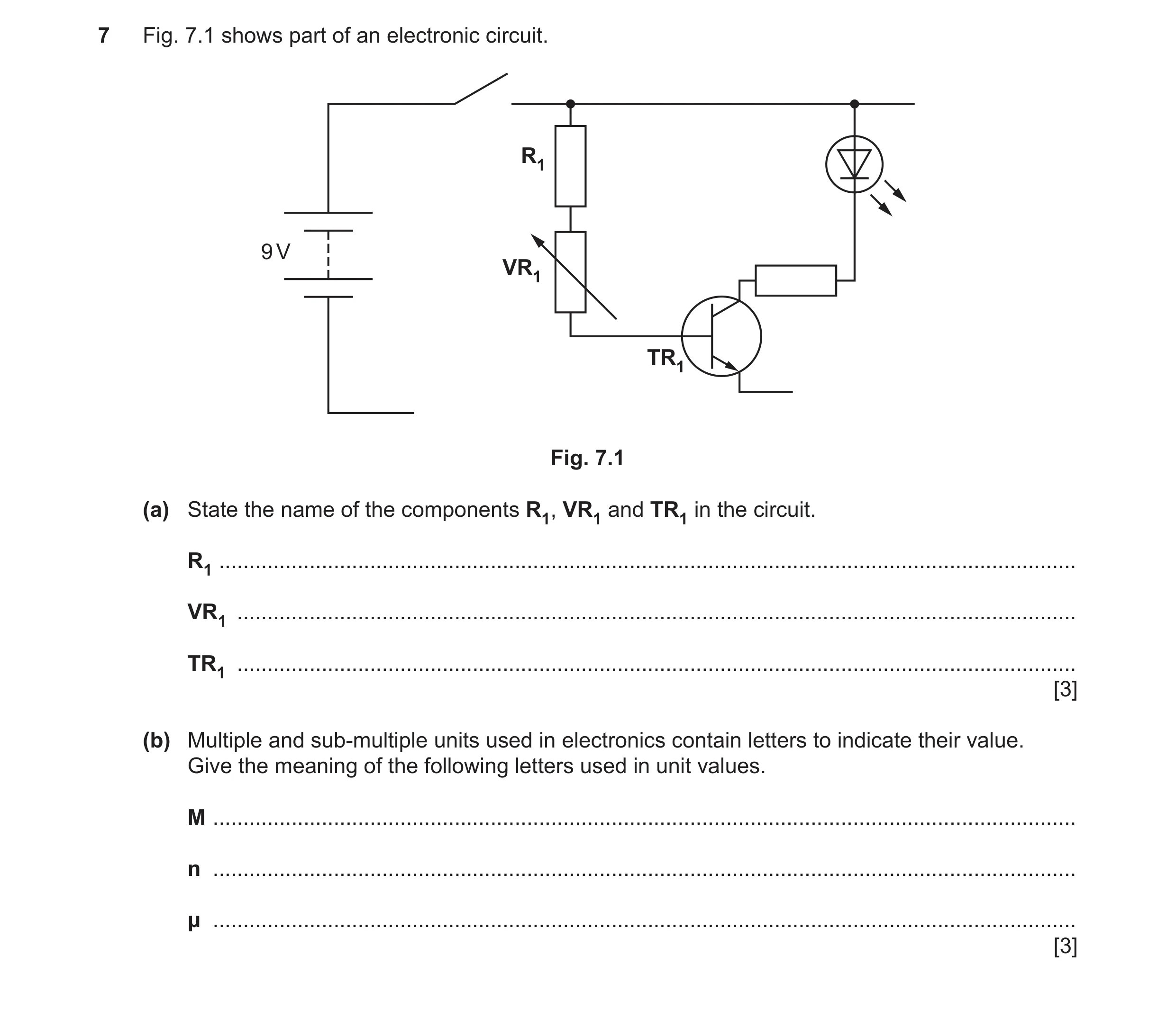
![Question 133: Use sketches and notes to describe how a reed switch is operated. [2]](https://img.pastlit.com/crops/c9cec639-fa30-4ff6-806d-f8c6a7fff804/q8.webp) 147 / 198
147 / 198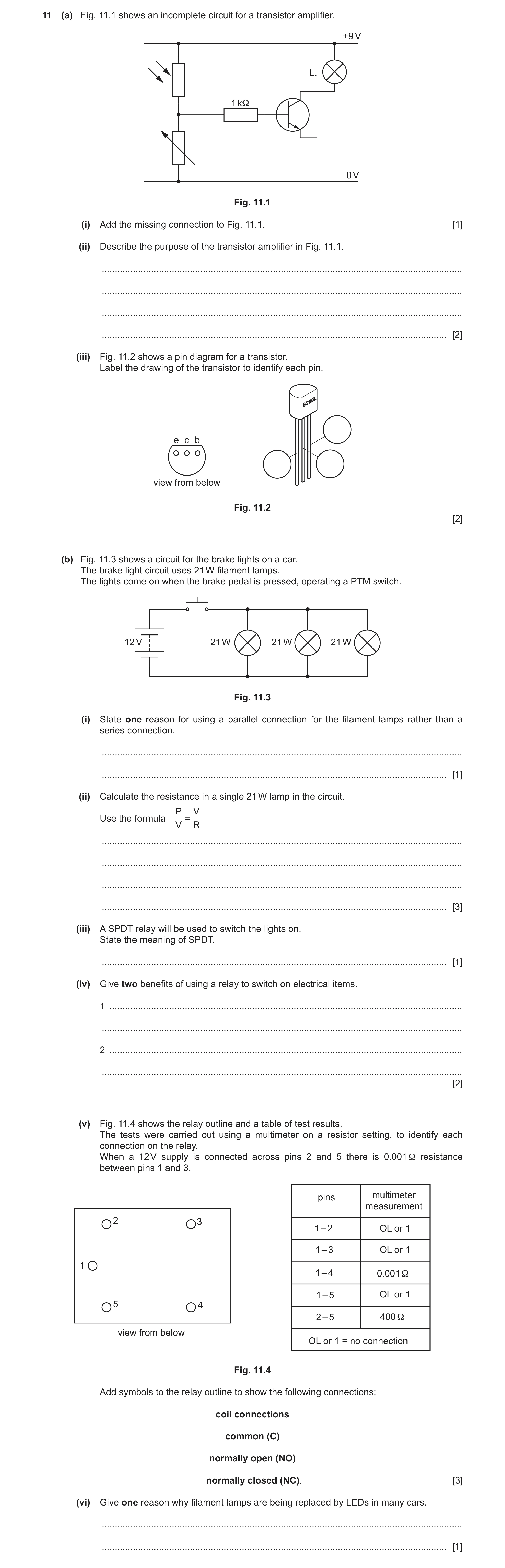
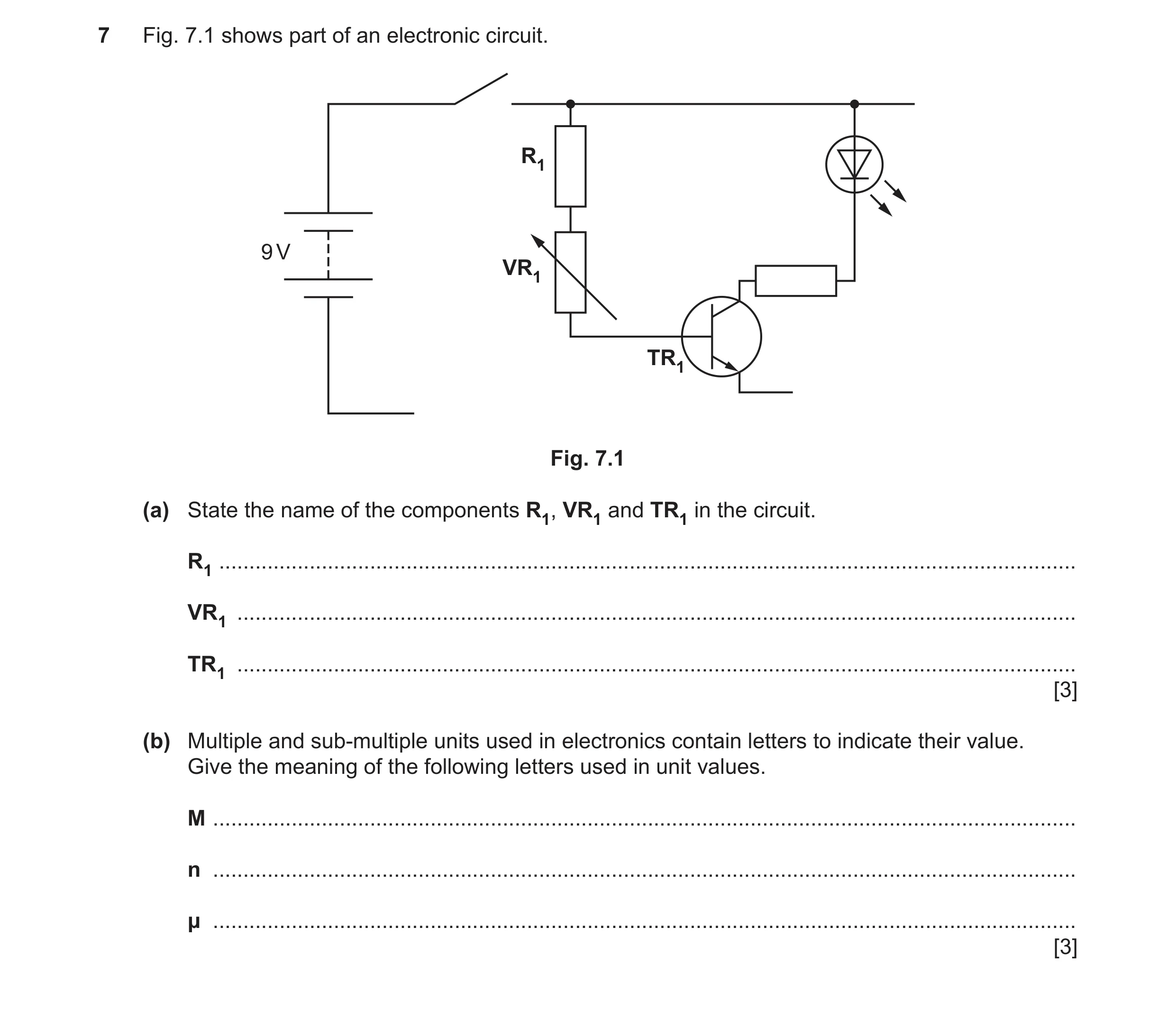
![Question 136: Use sketches and notes to describe how a reed switch is operated. [2]](https://img.pastlit.com/crops/1e2a17ef-1dec-4447-8eb3-d123ff8c29da/q8.webp) 151 / 198
151 / 198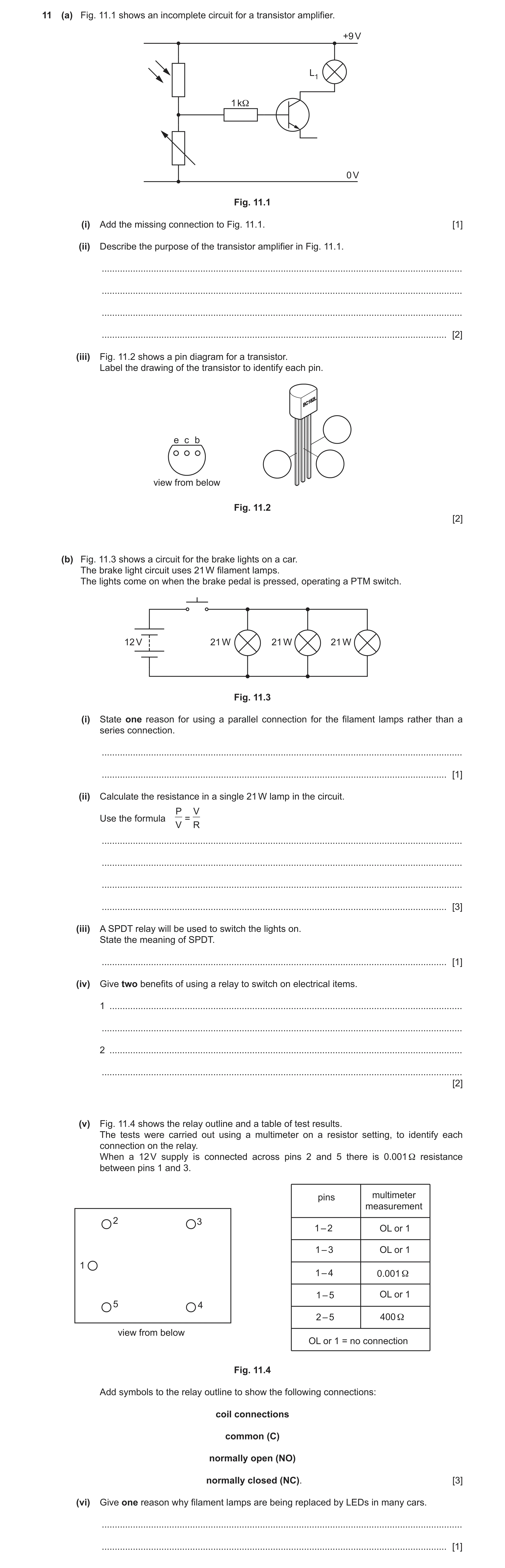
 154 / 198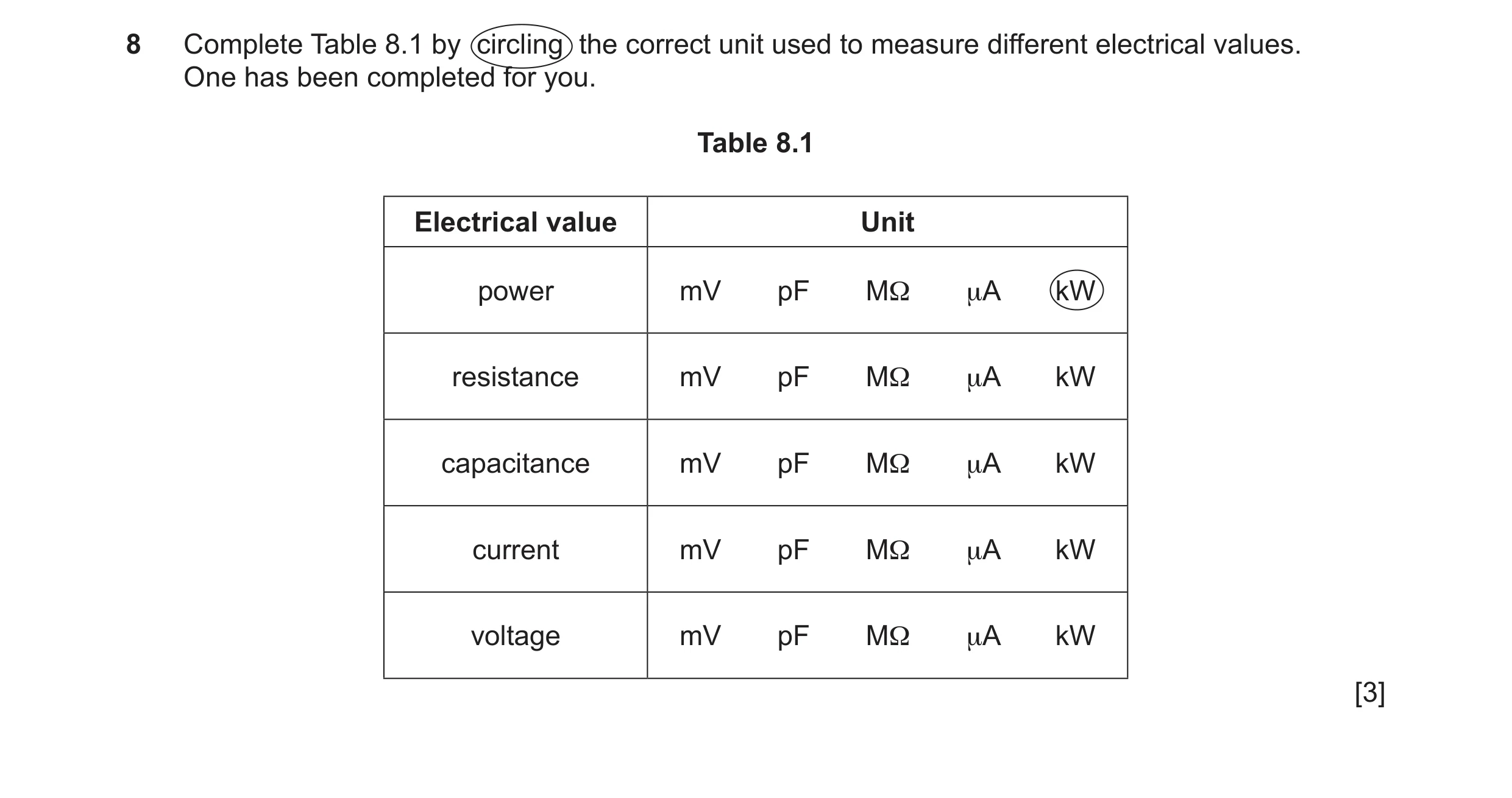
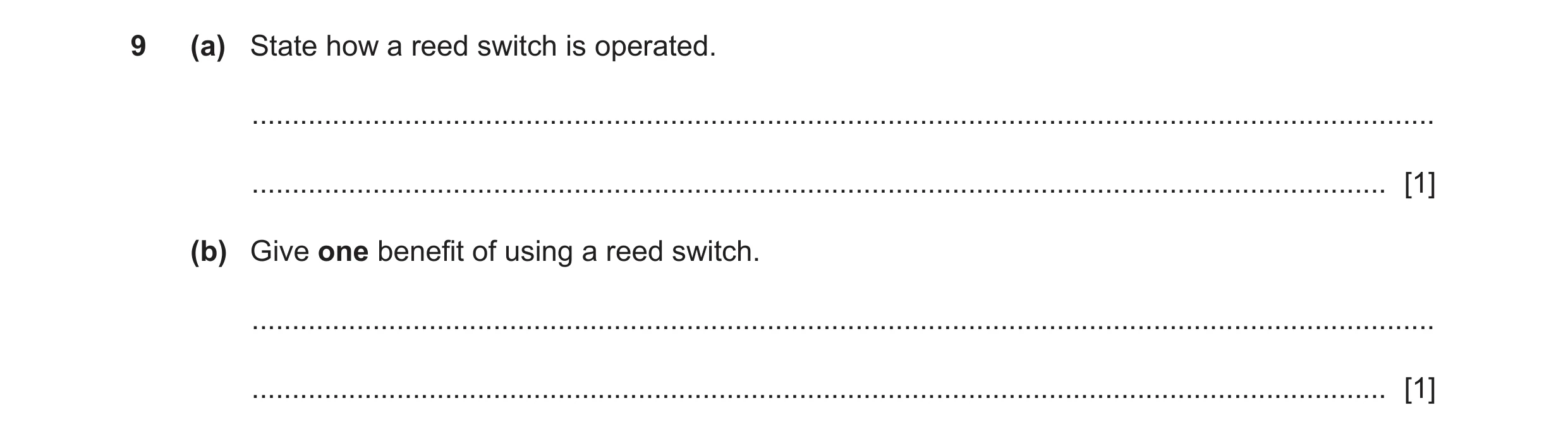 155 / 198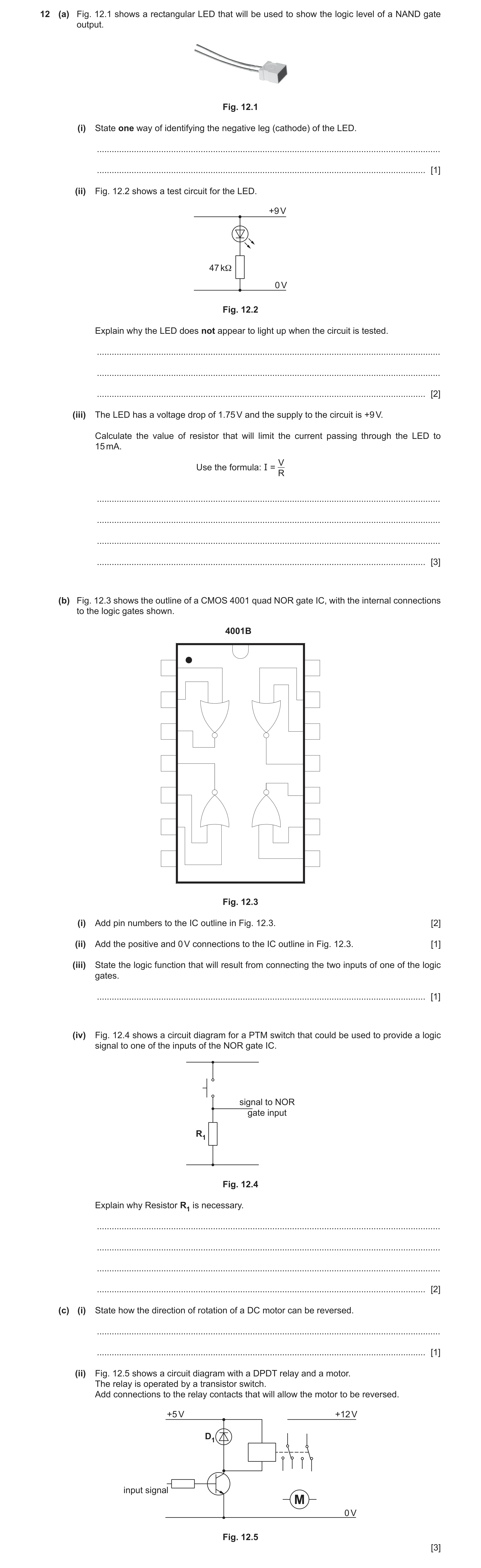
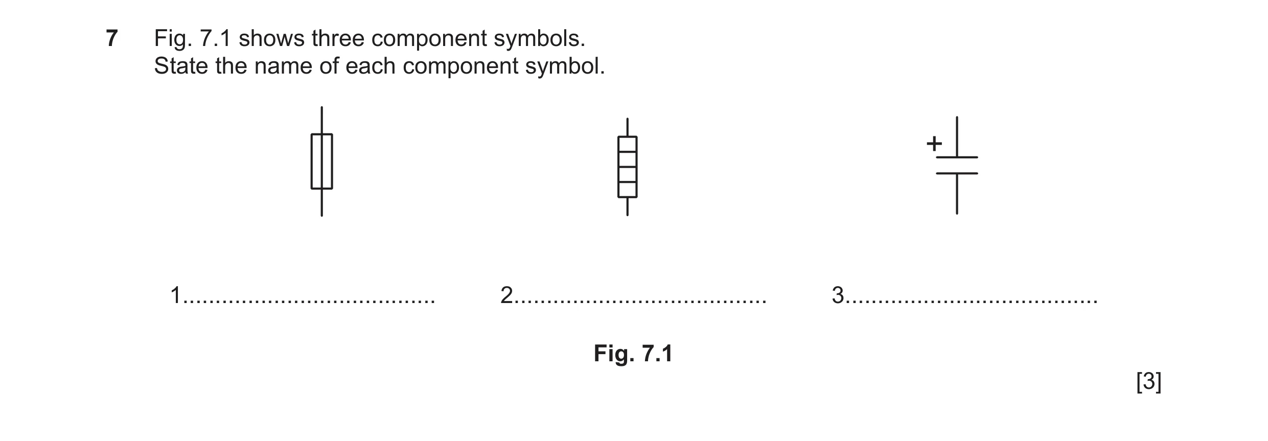
![Question 143: Fig. 8.1 shows two battery symbols. 9V 9V Fig. 8.1 (a) Draw parallel connections between the two batteries. [1] (b) State the output voltag…](https://img.pastlit.com/crops/dbaedf40-def3-4f35-8105-16151290898d/q8.webp) 158 / 198
158 / 198![Question 144: Complete Table 9.1 by adding the missing values. Table 9.1 Value in multiple units Value in ohms (Ω) 5 kΩ Ω 0.27 kΩ Ω 3 MΩ Ω [3]](https://img.pastlit.com/crops/dbaedf40-def3-4f35-8105-16151290898d/q9.webp) 159 / 198
159 / 198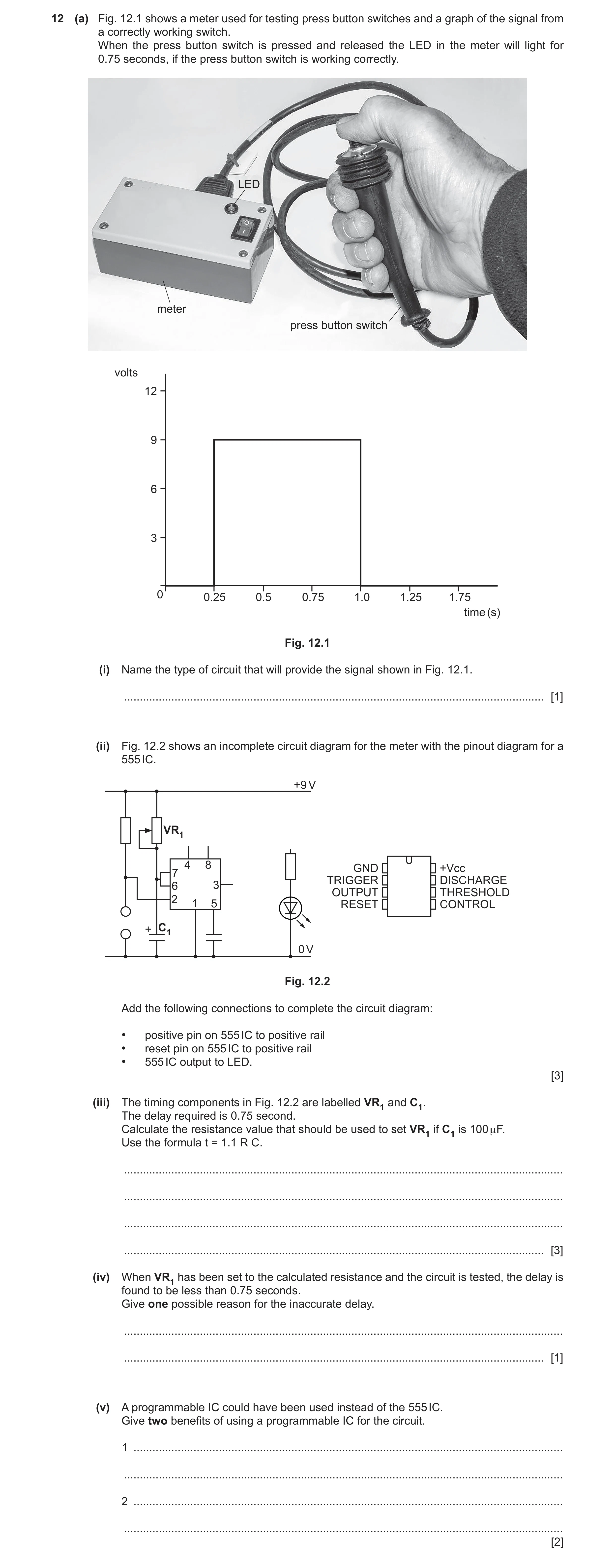

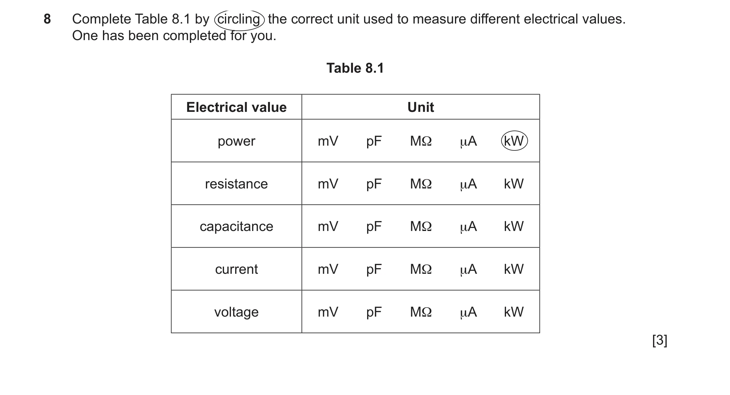
 161 / 198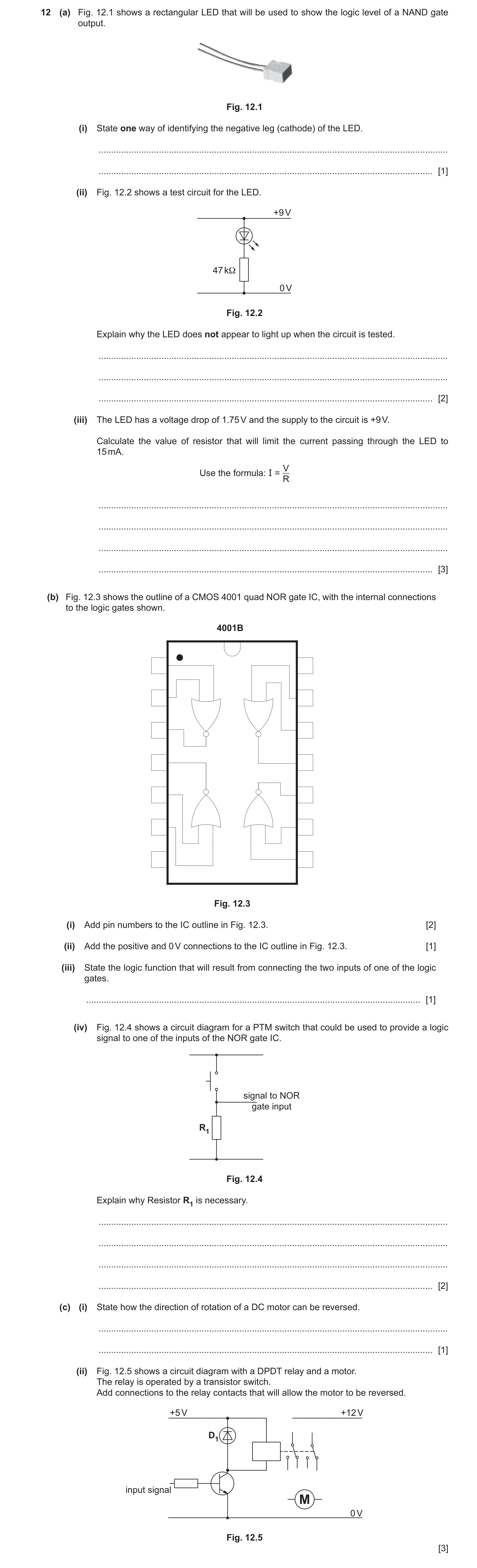
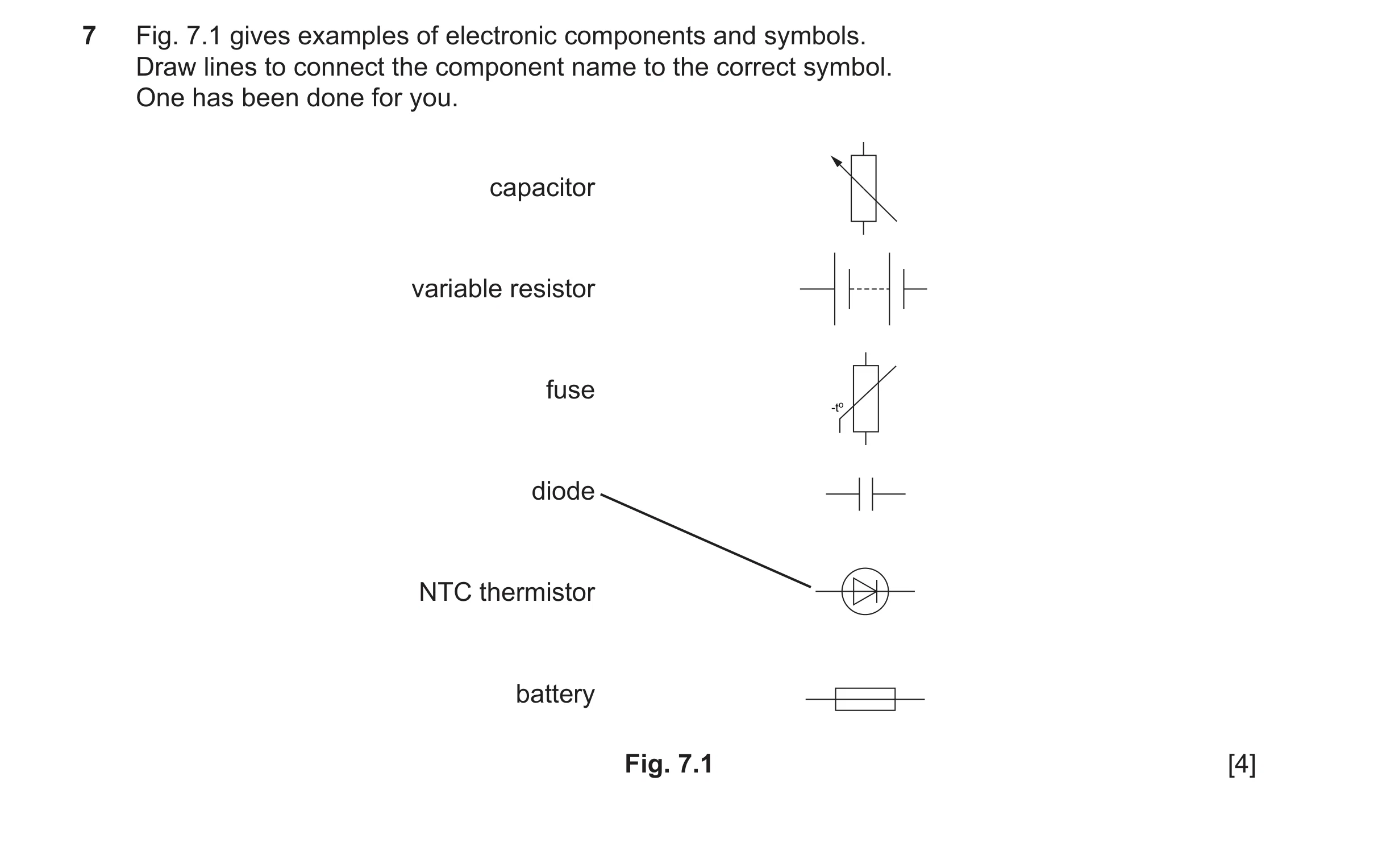 164 / 198
 165 / 198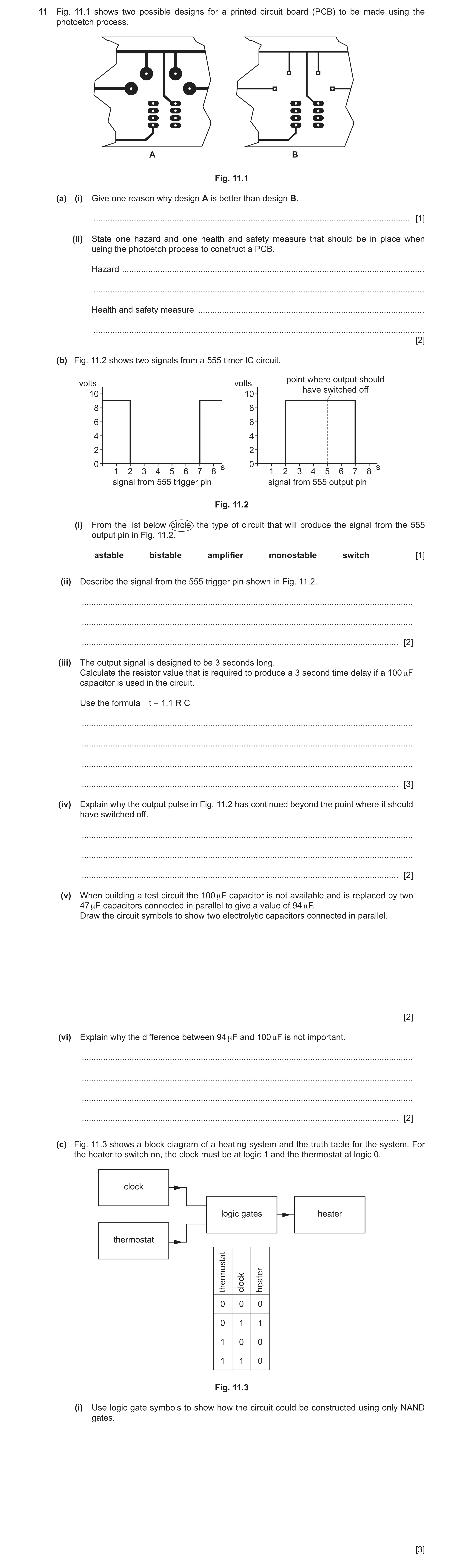
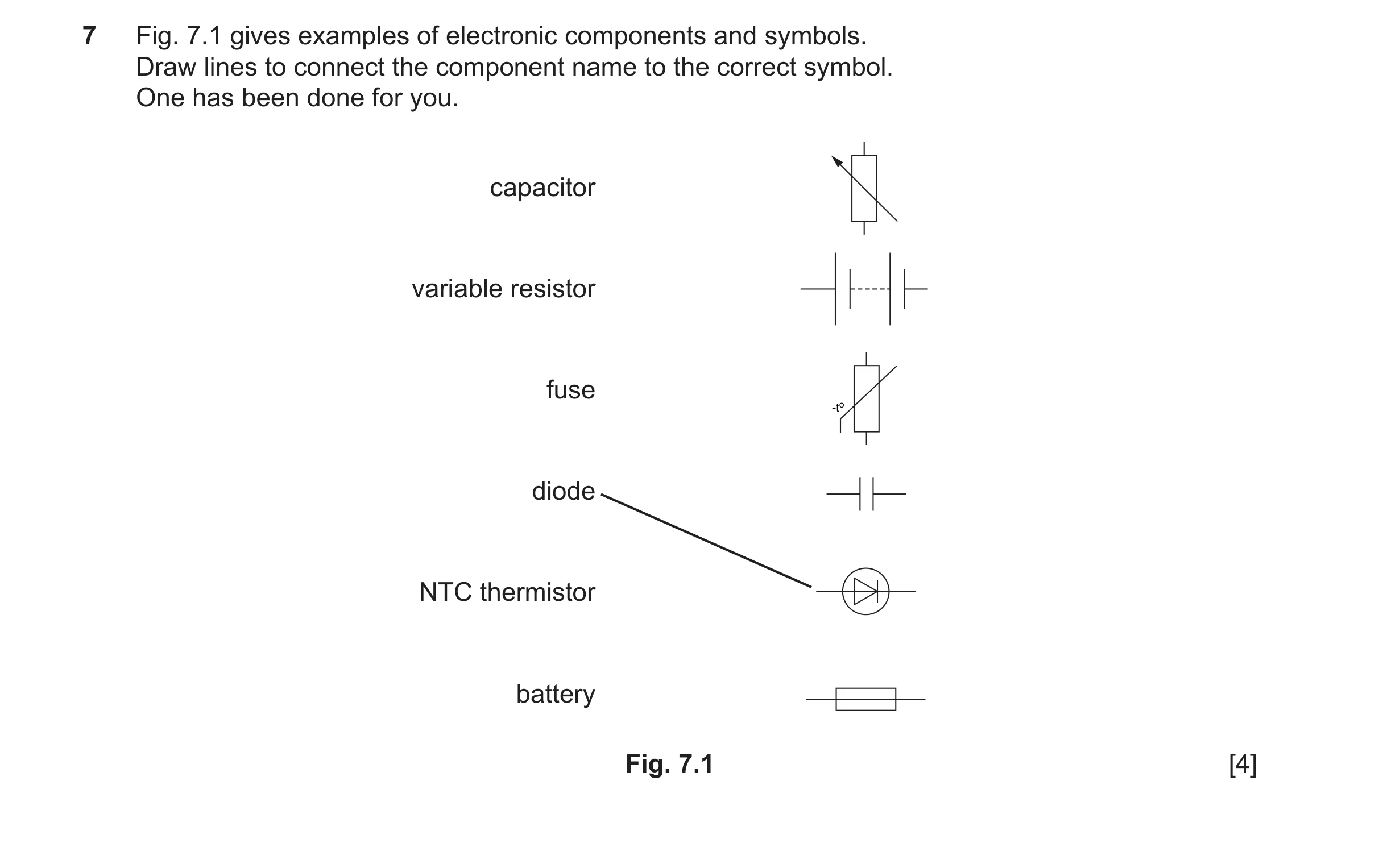
 168 / 198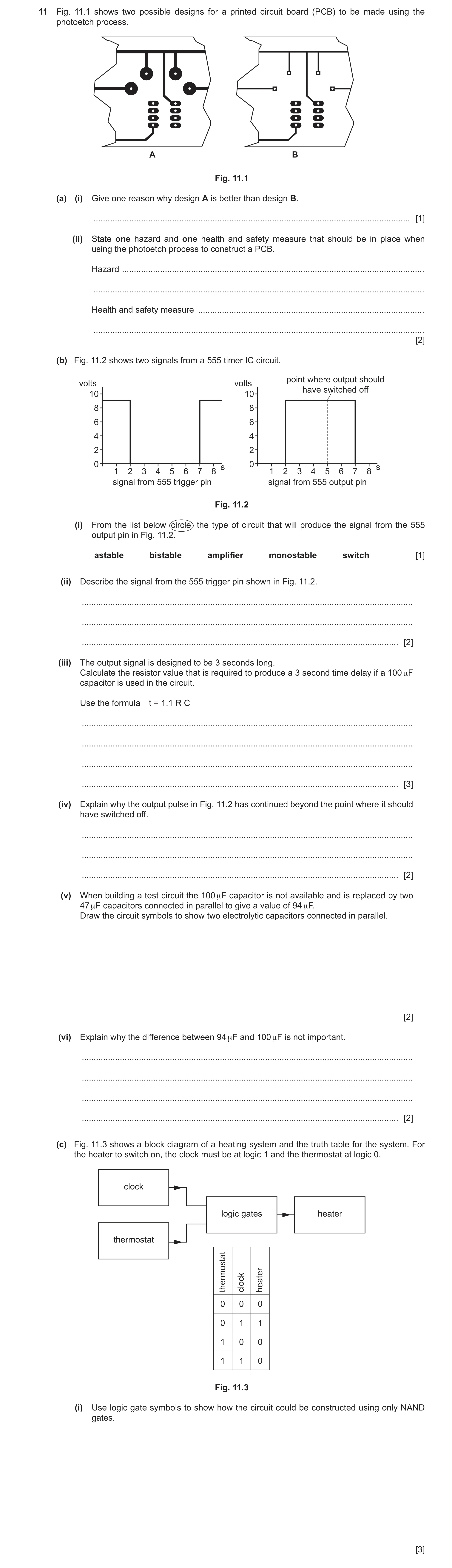
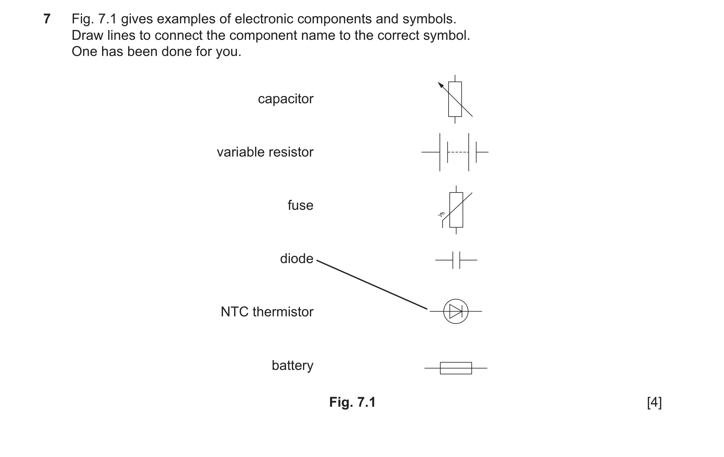
 172 / 198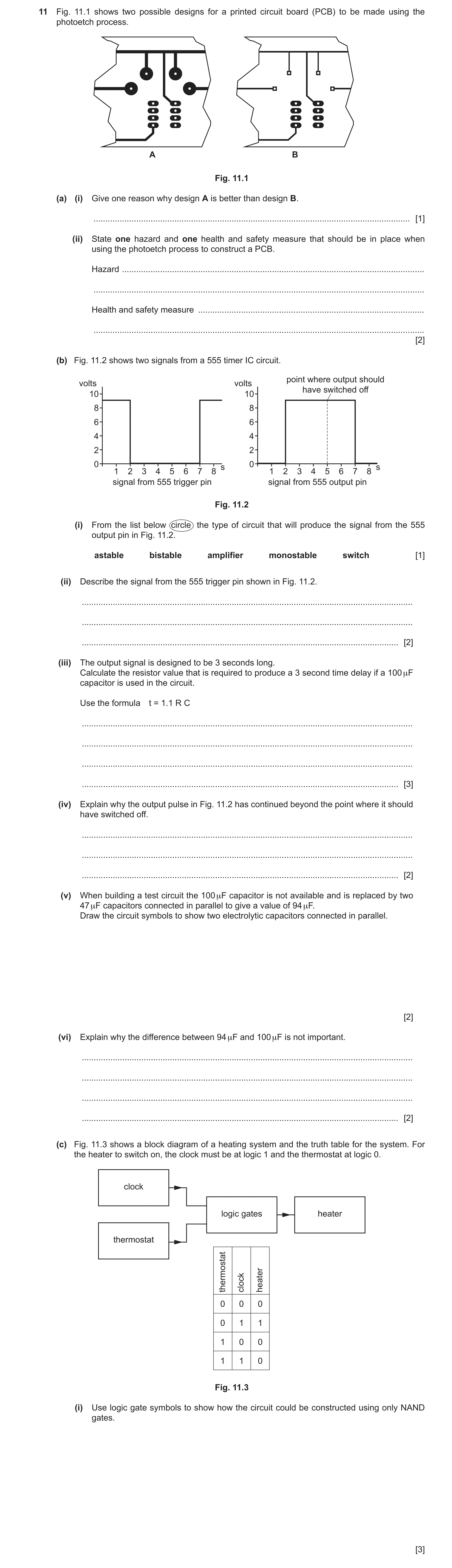
 175 / 198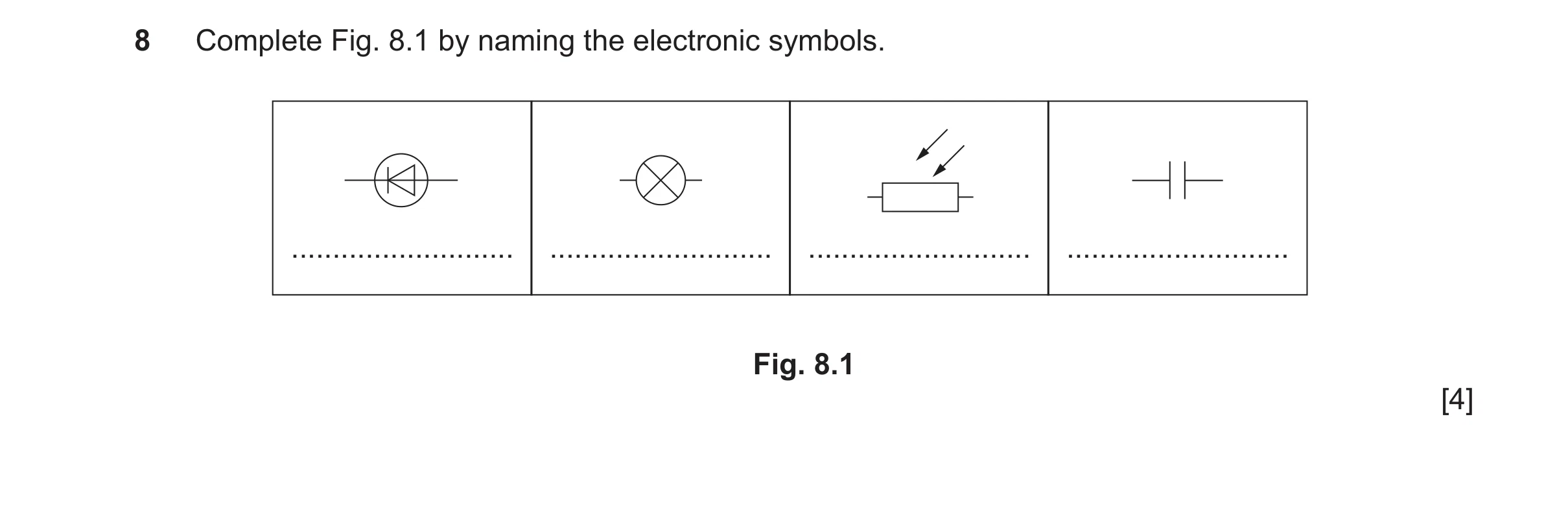
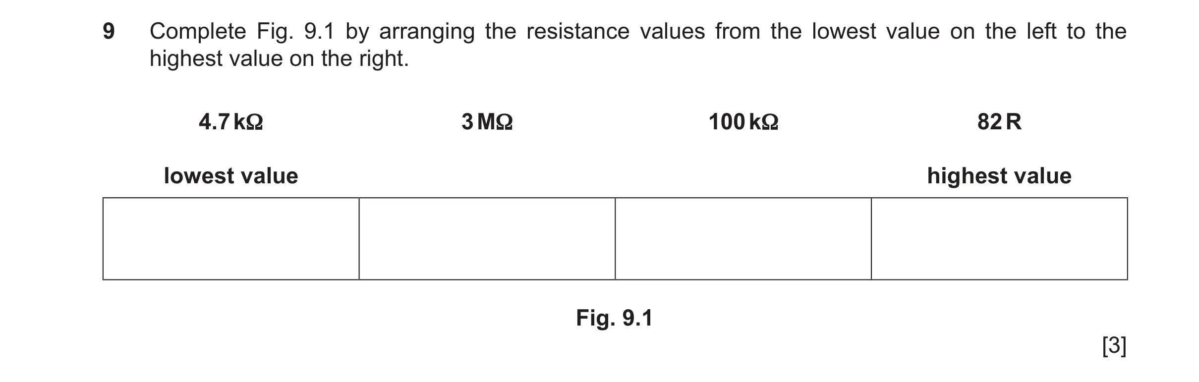 176 / 198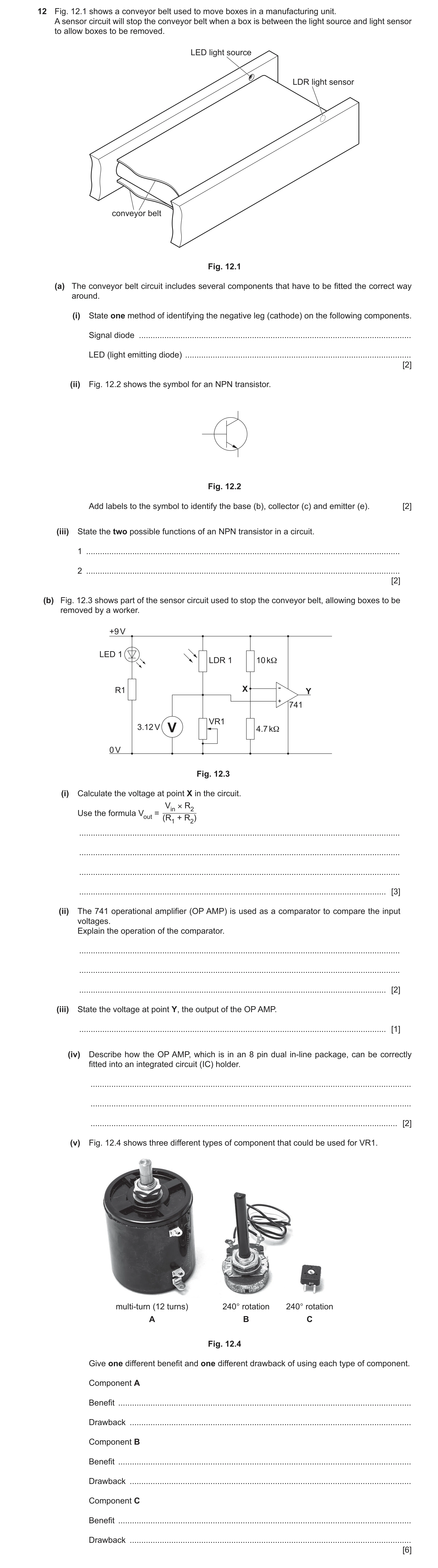
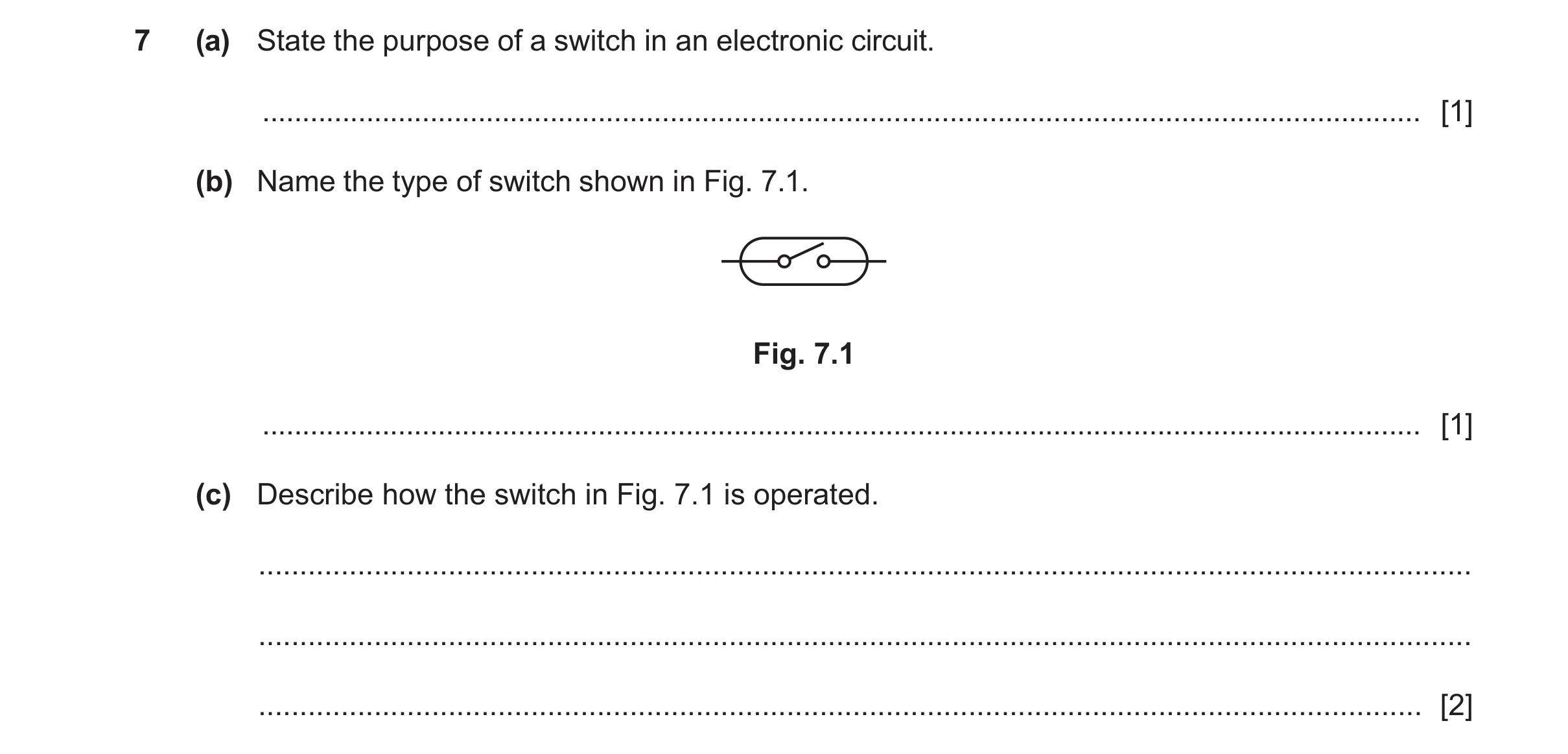
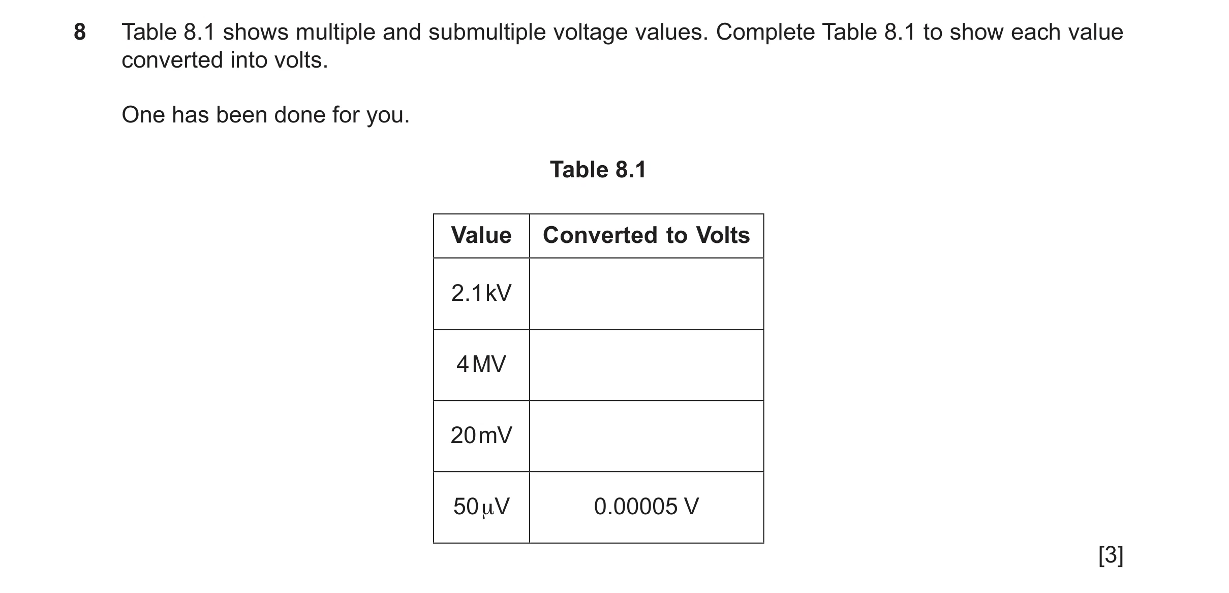 180 / 198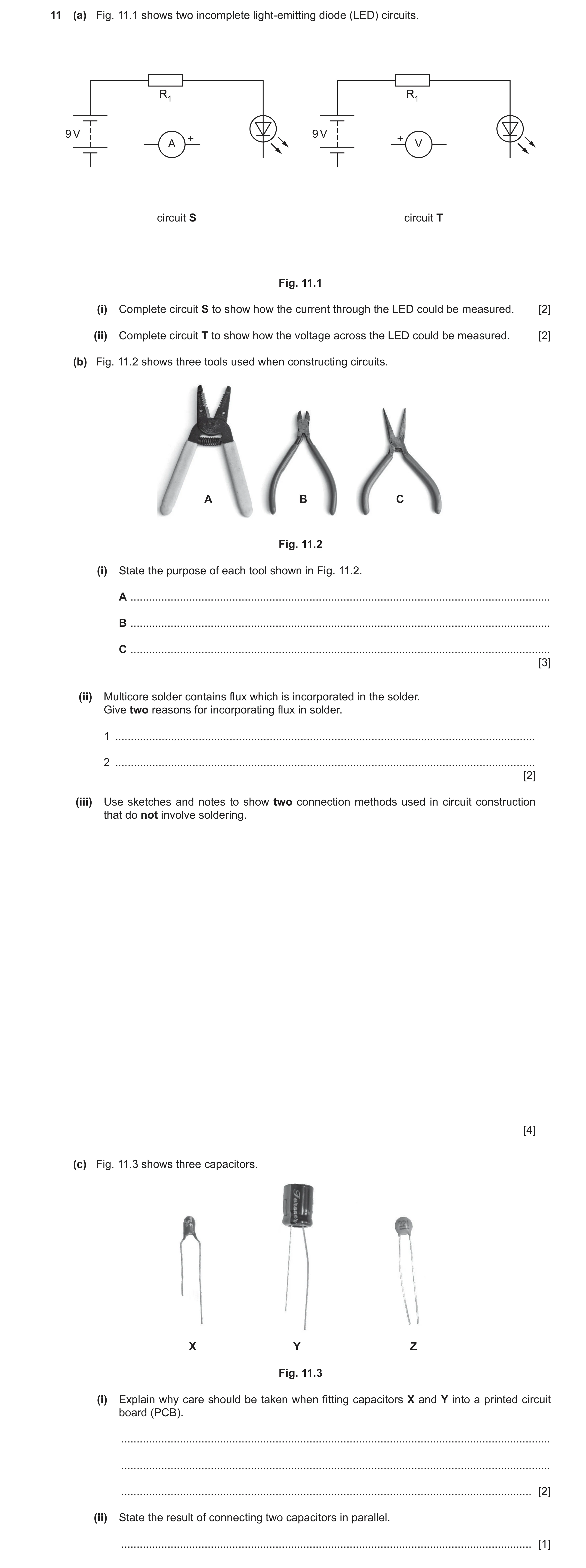
 182 / 198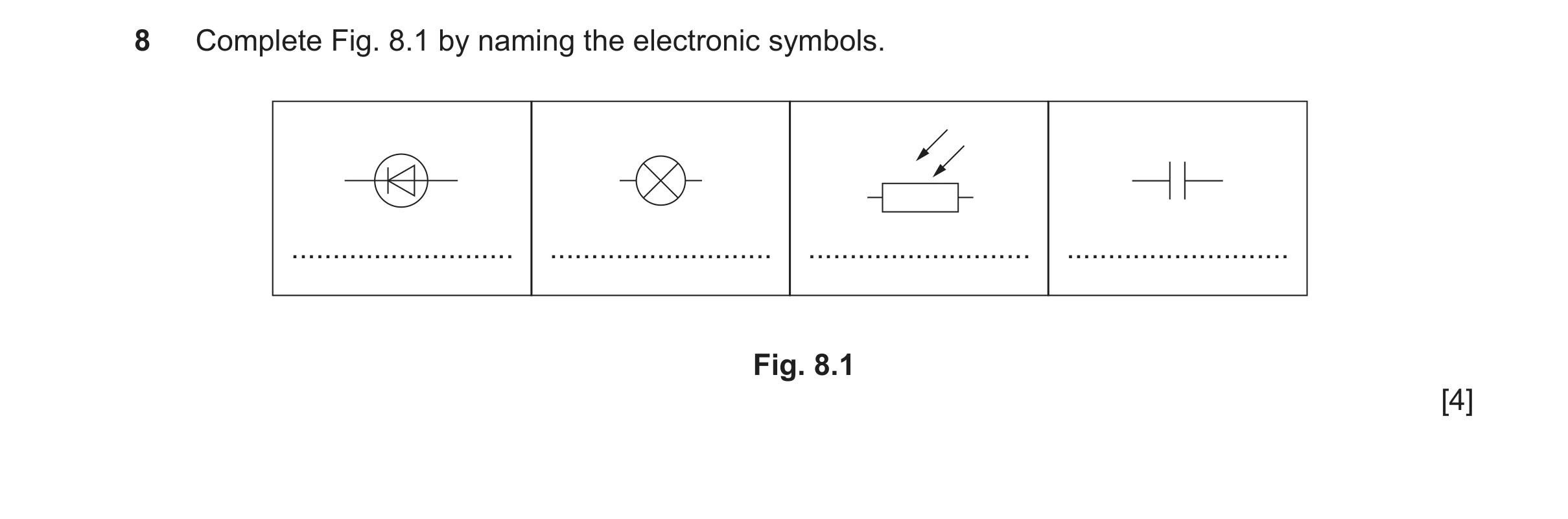
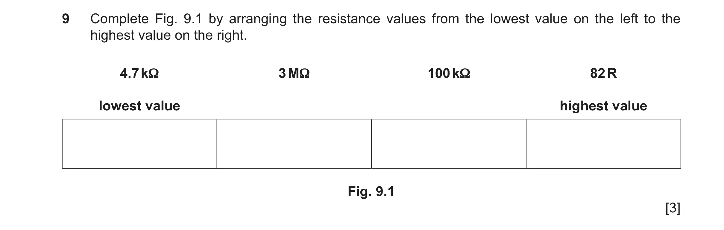 183 / 198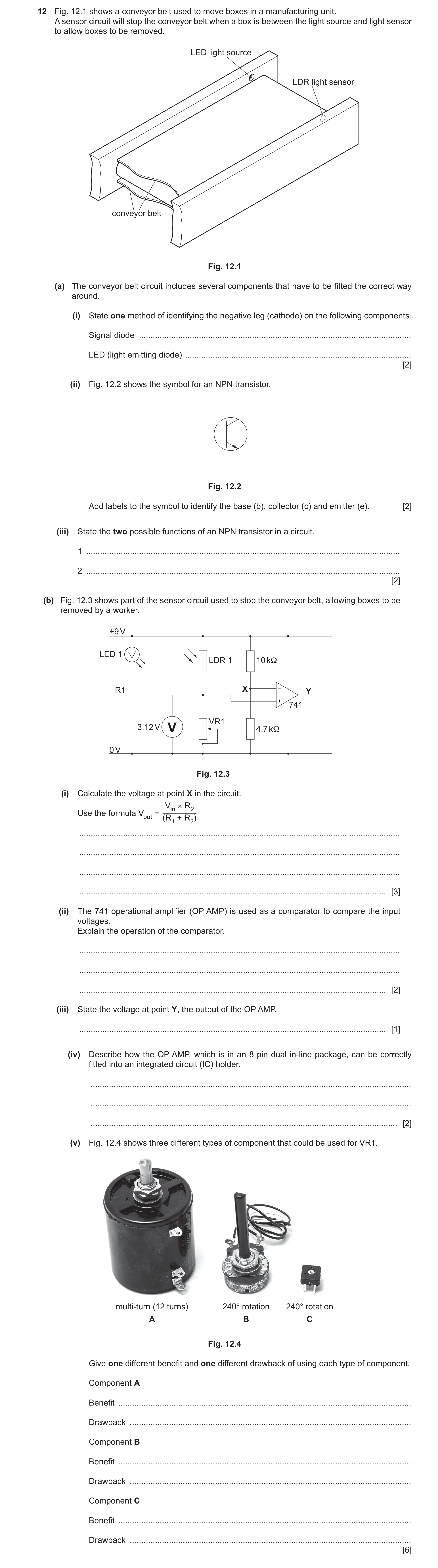
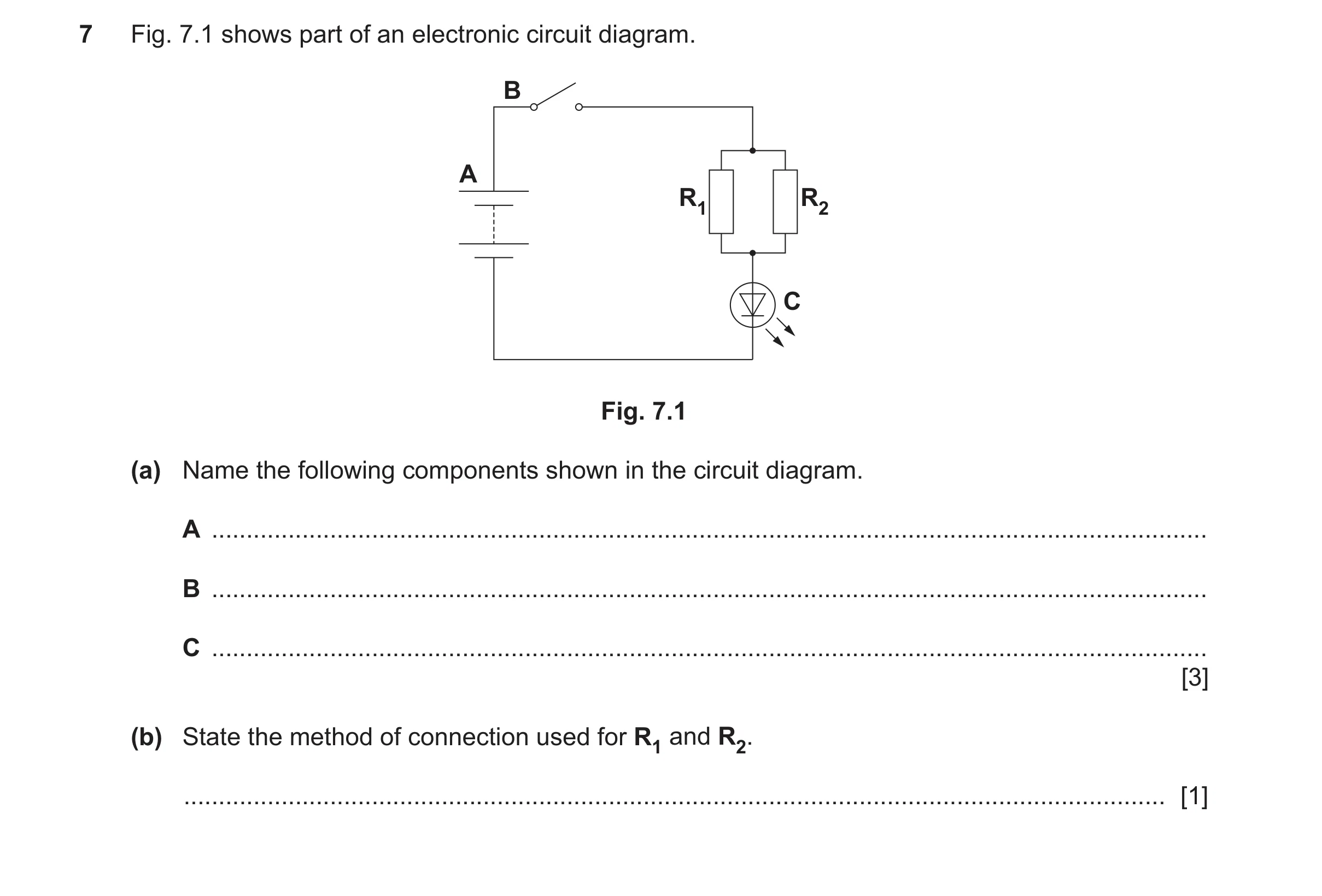

 187 / 198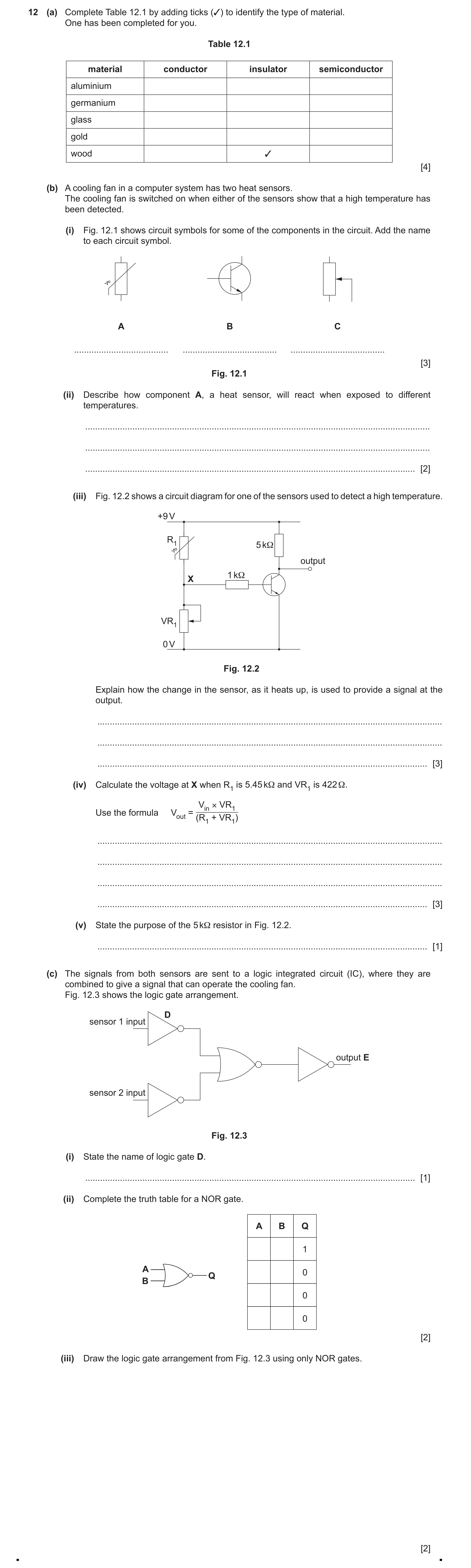
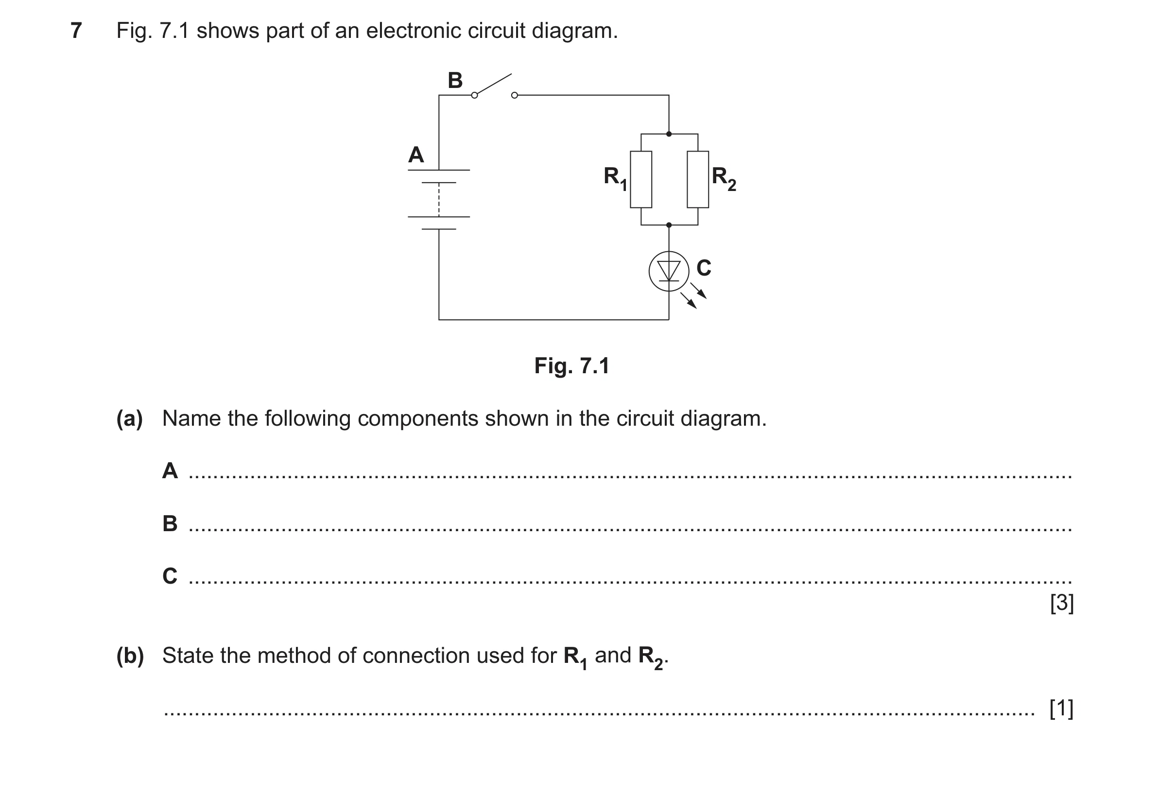

 191 / 198

 195 / 198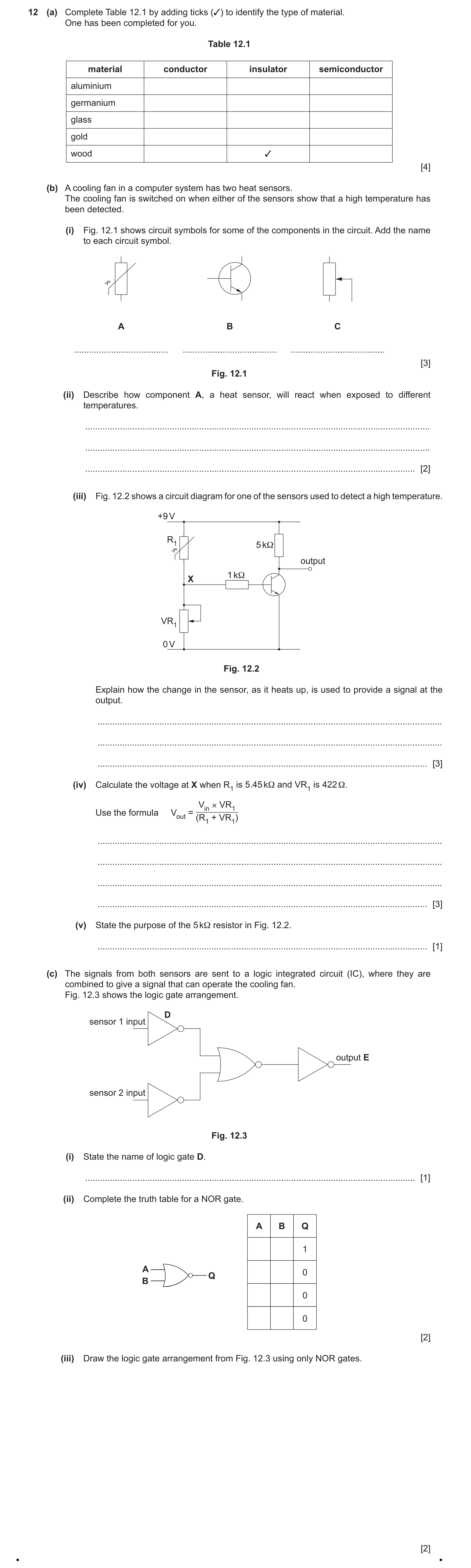
 2
2 3
3 3
3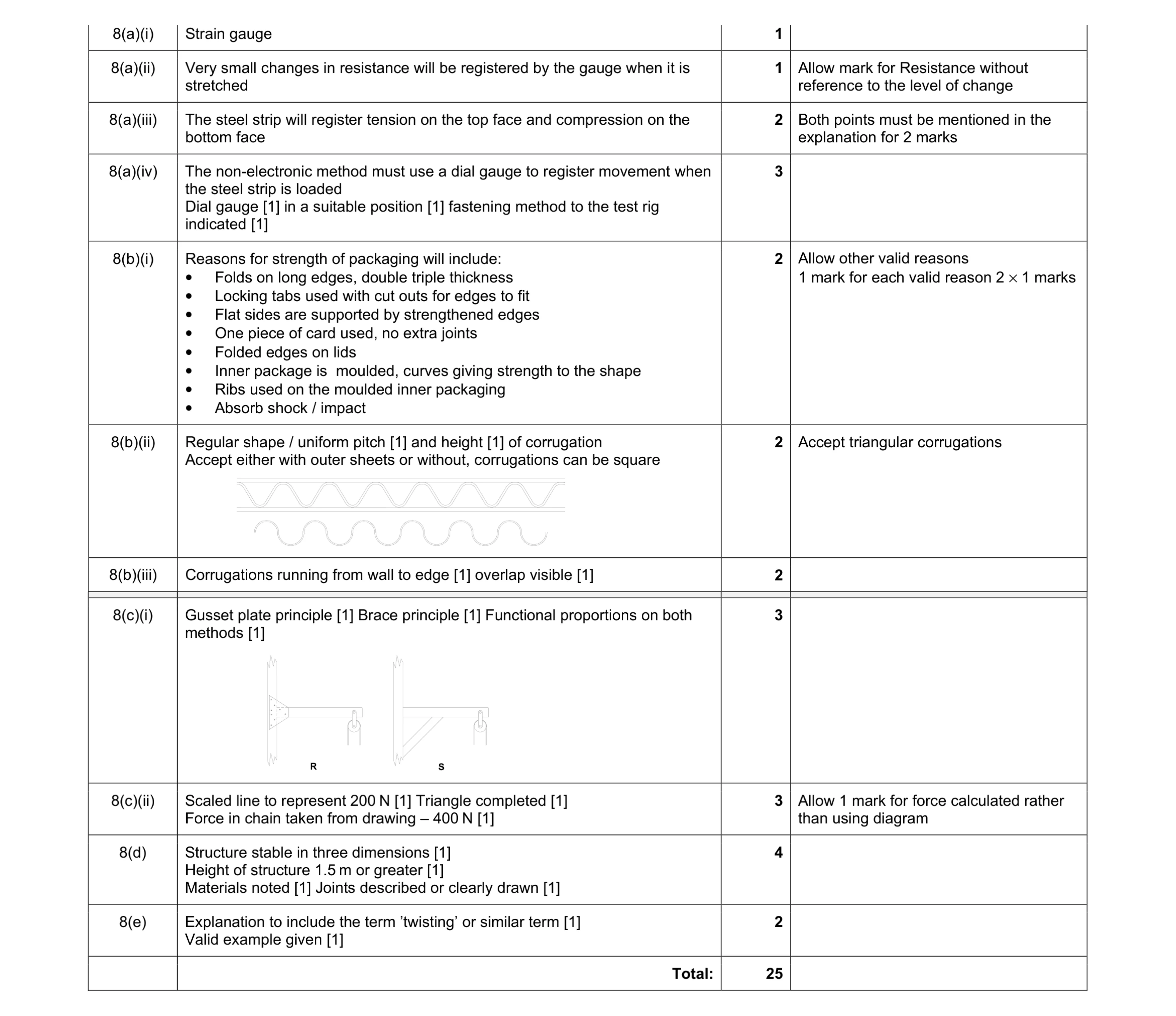 25
25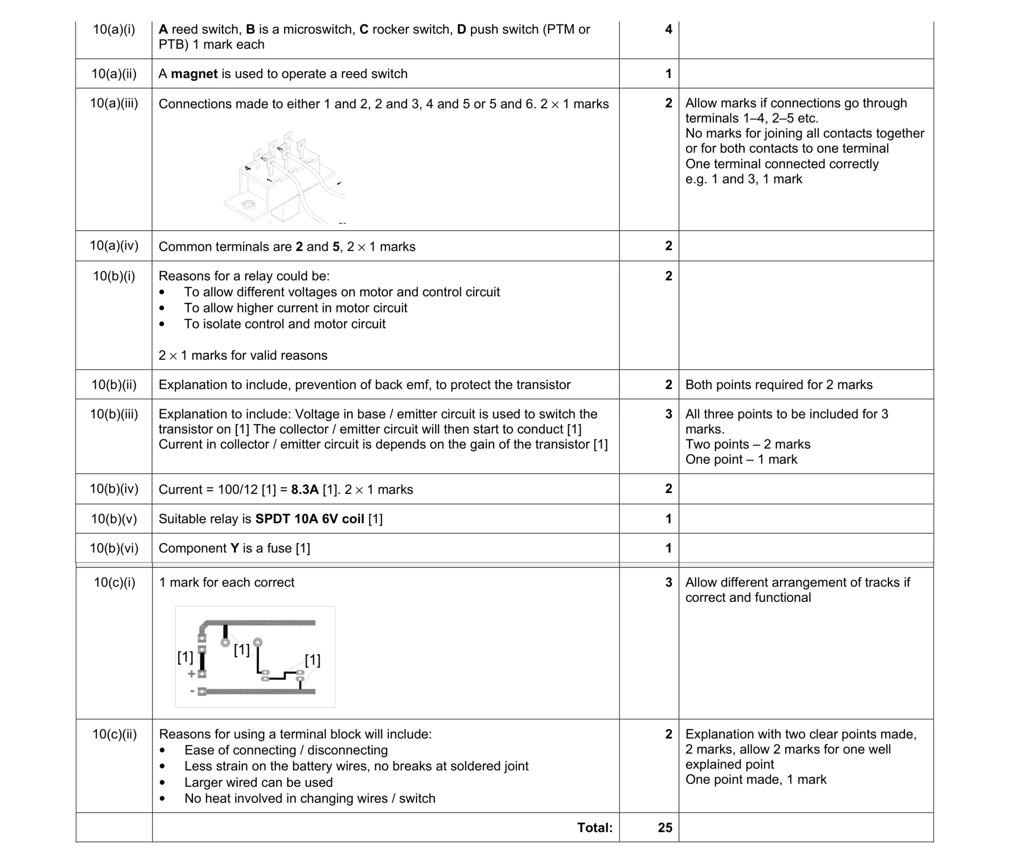 23
23 2
2 3
3 3
3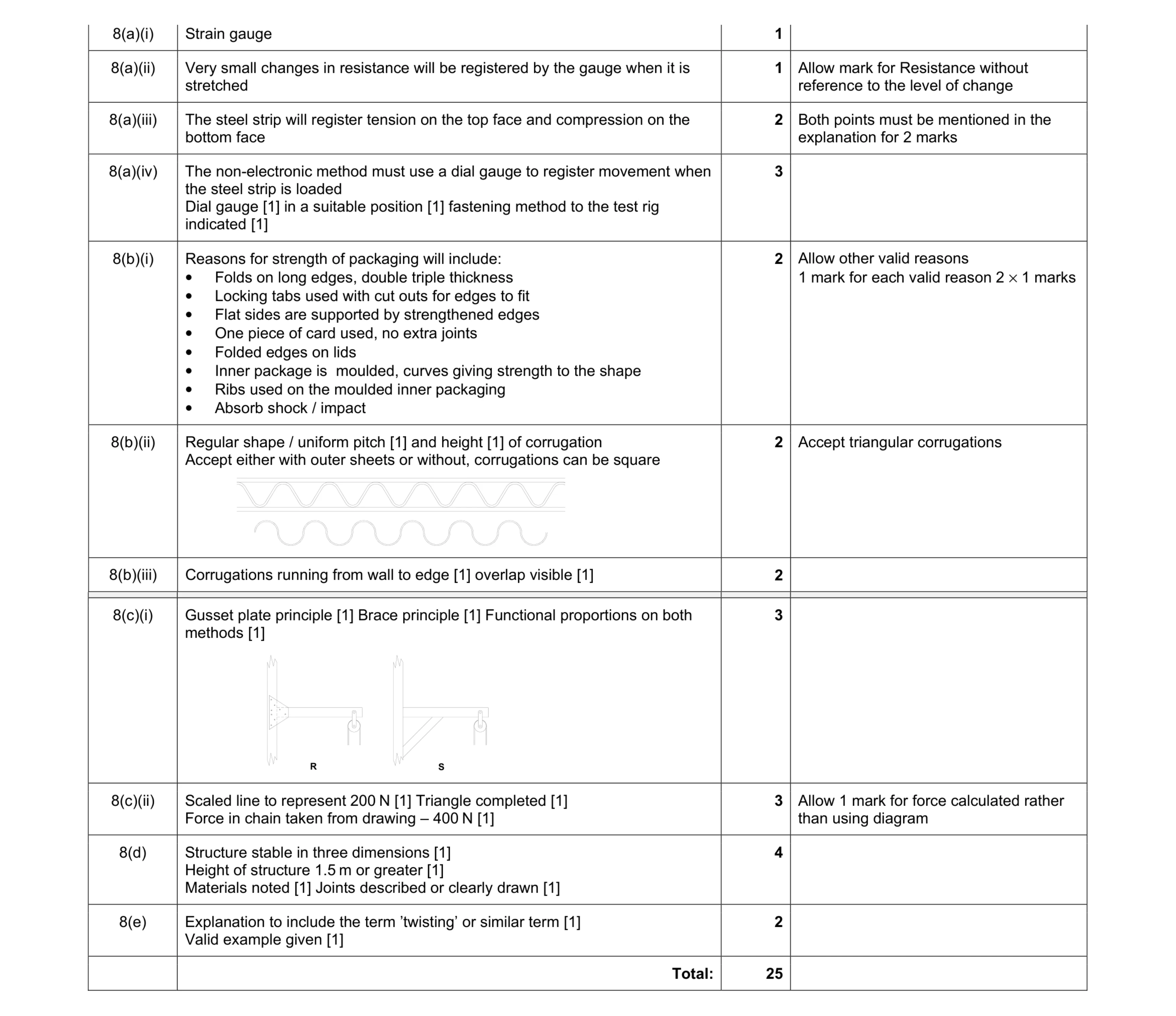 25
25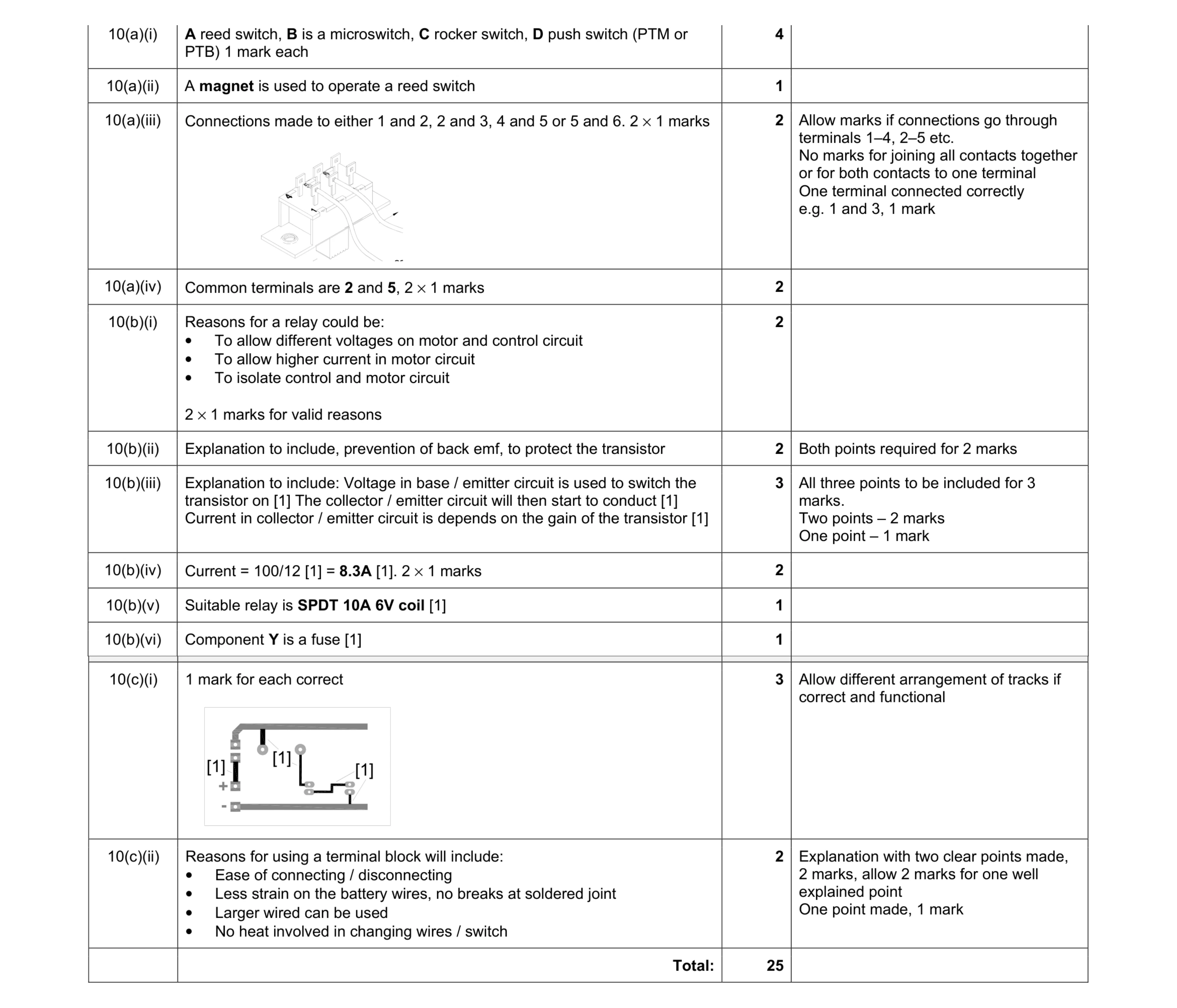 23
23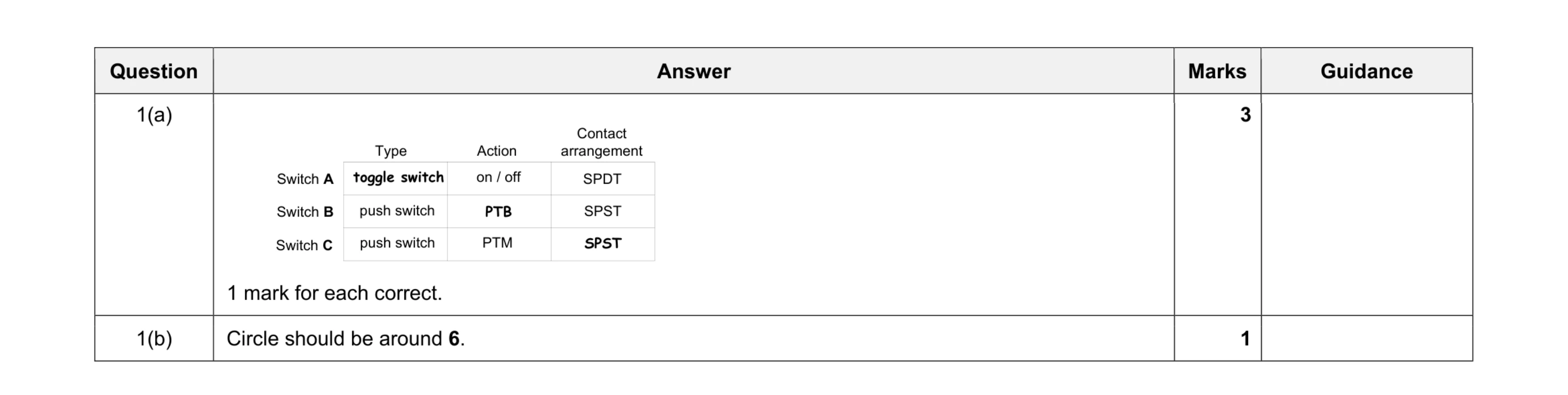 4
4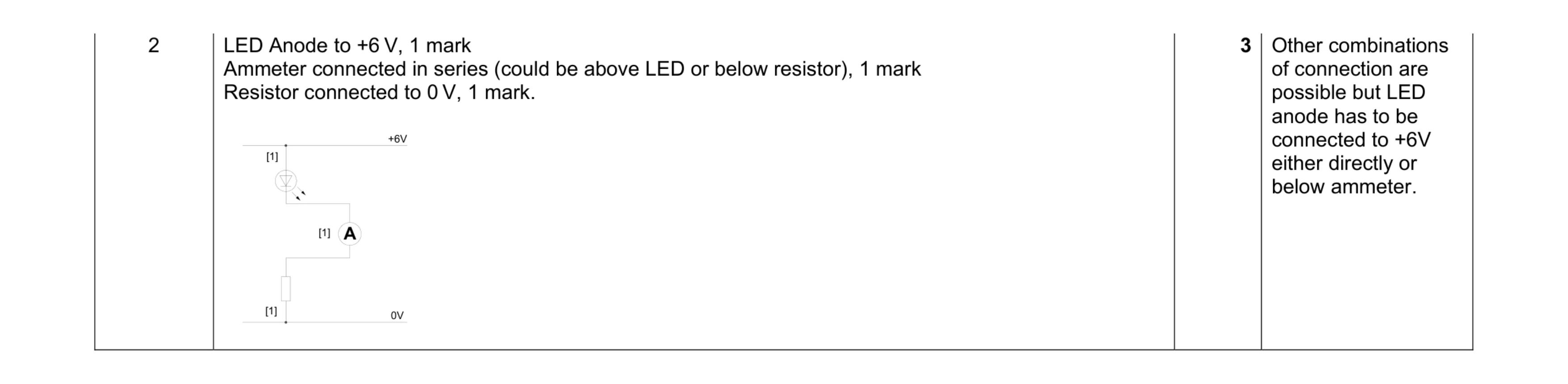 3
3 2
2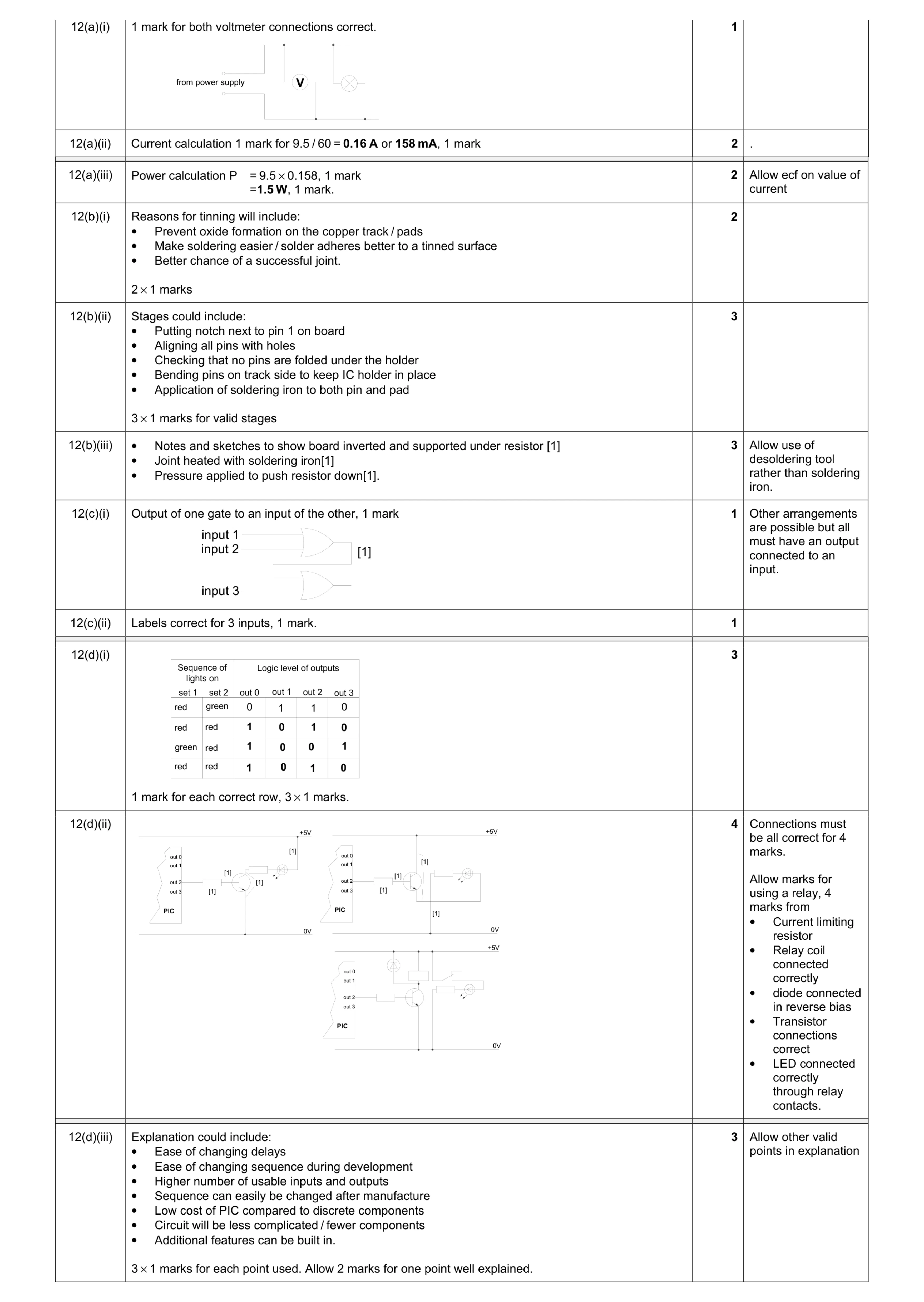 22
22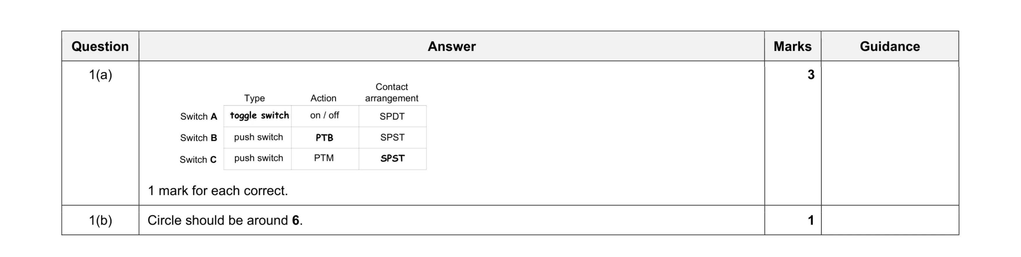 4
4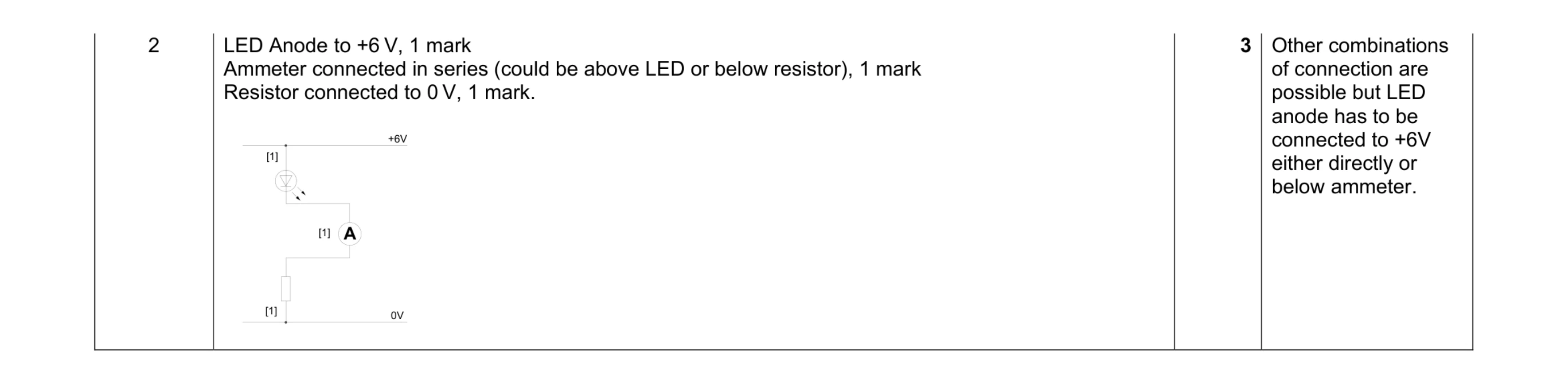 3
3 2
2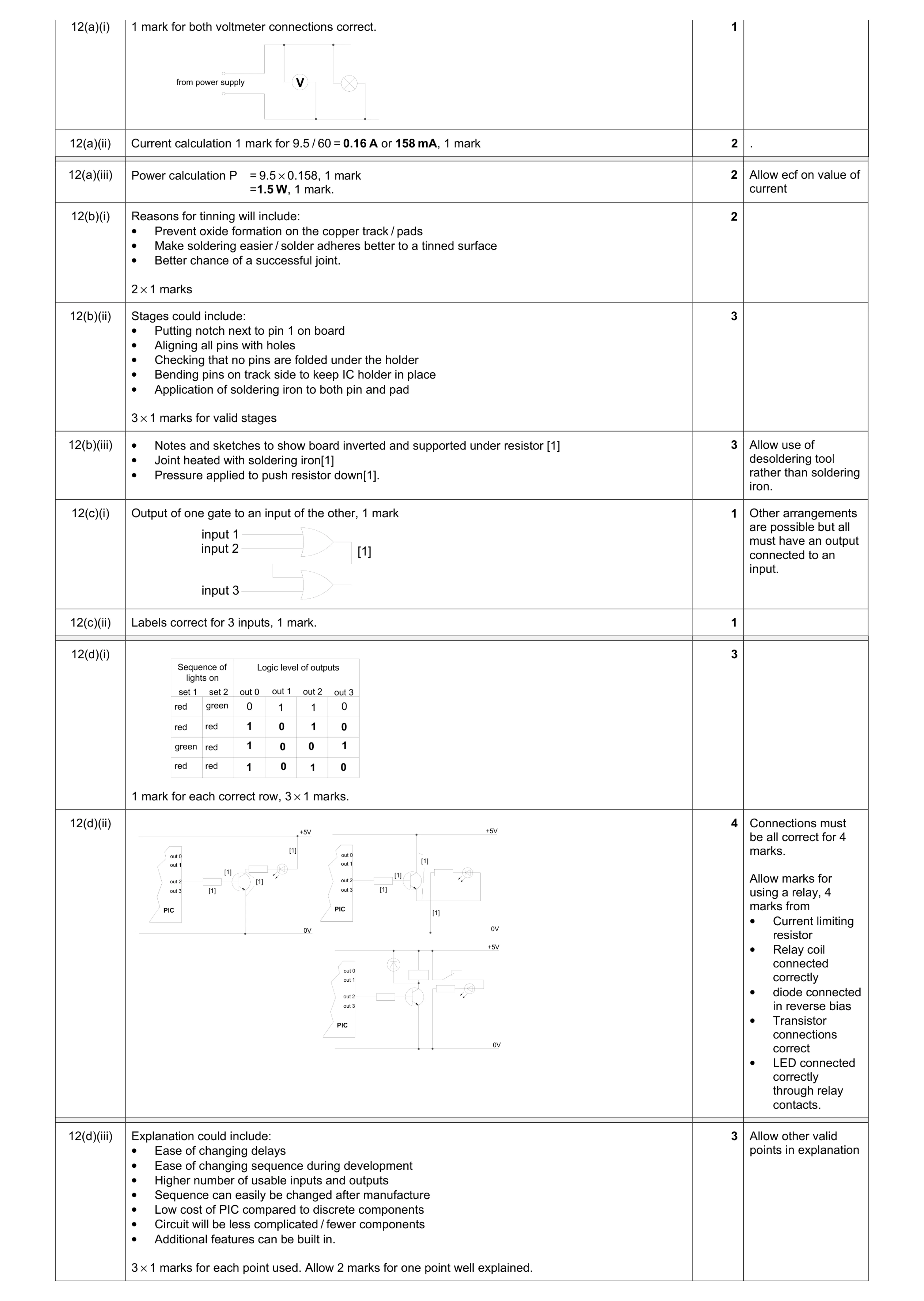 22
22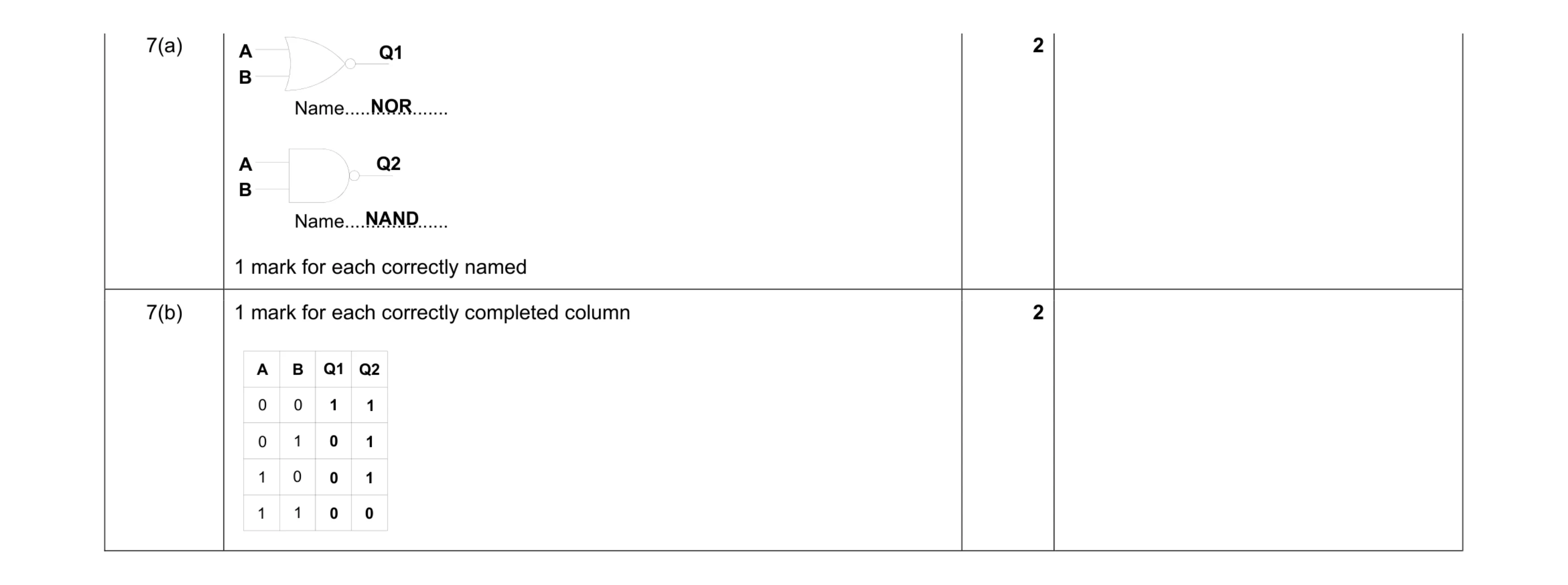 4
4 3
3 1
1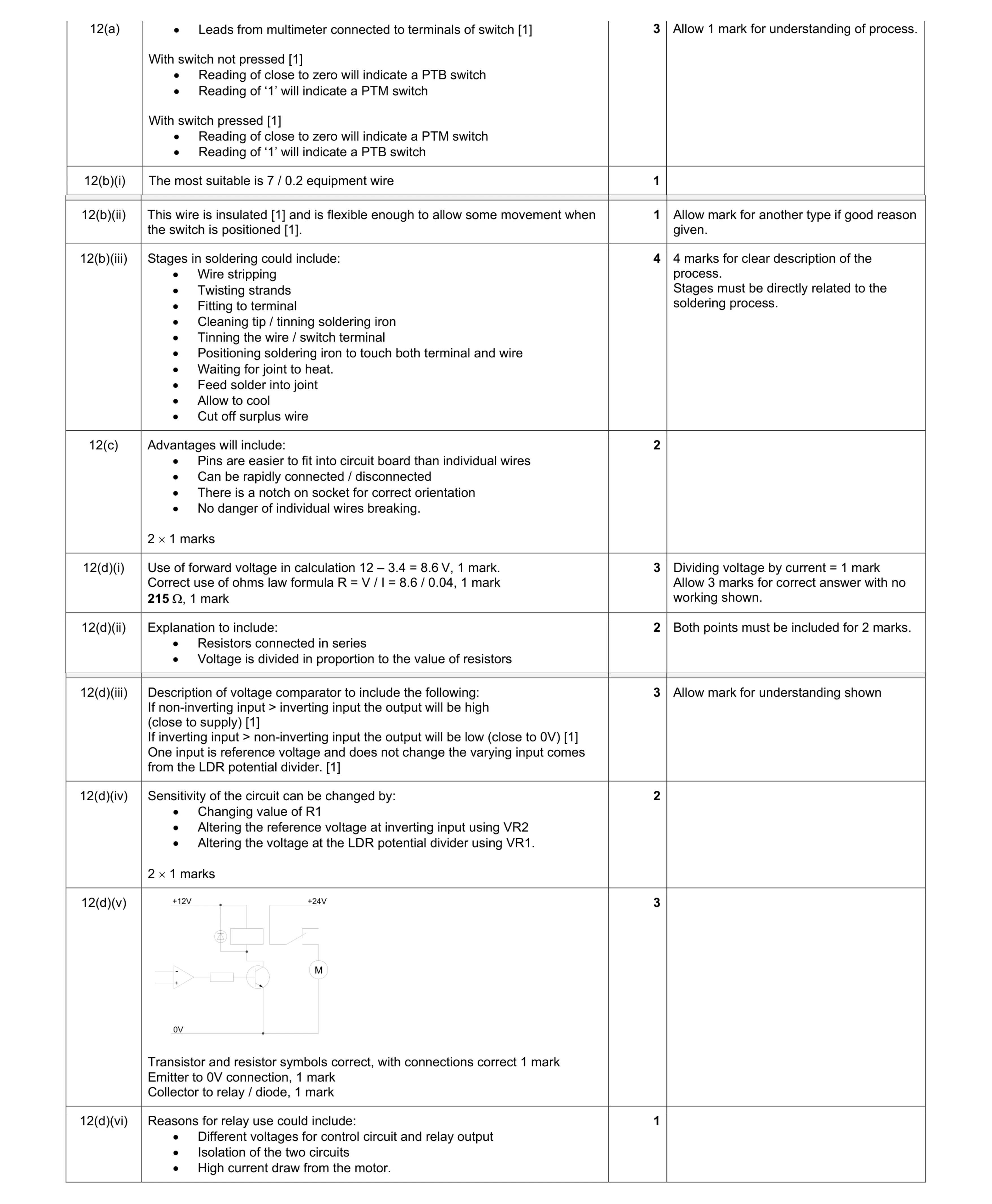 14
14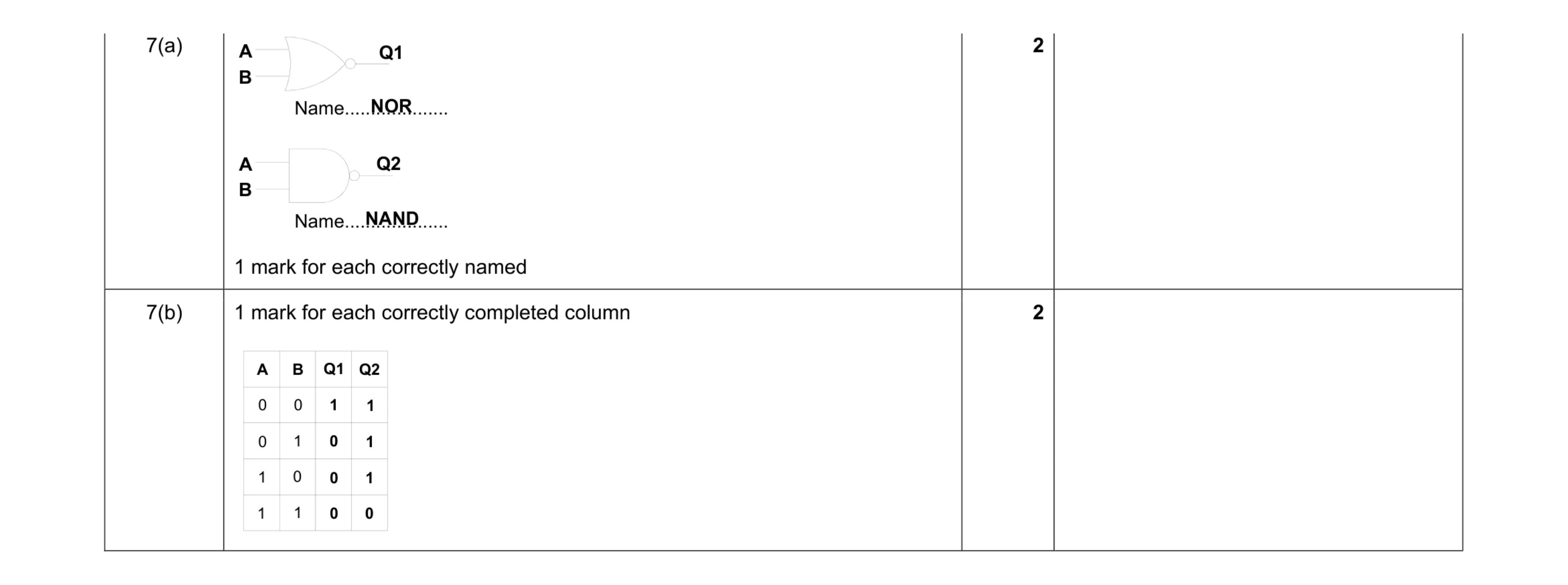 4
4 3
3 1
1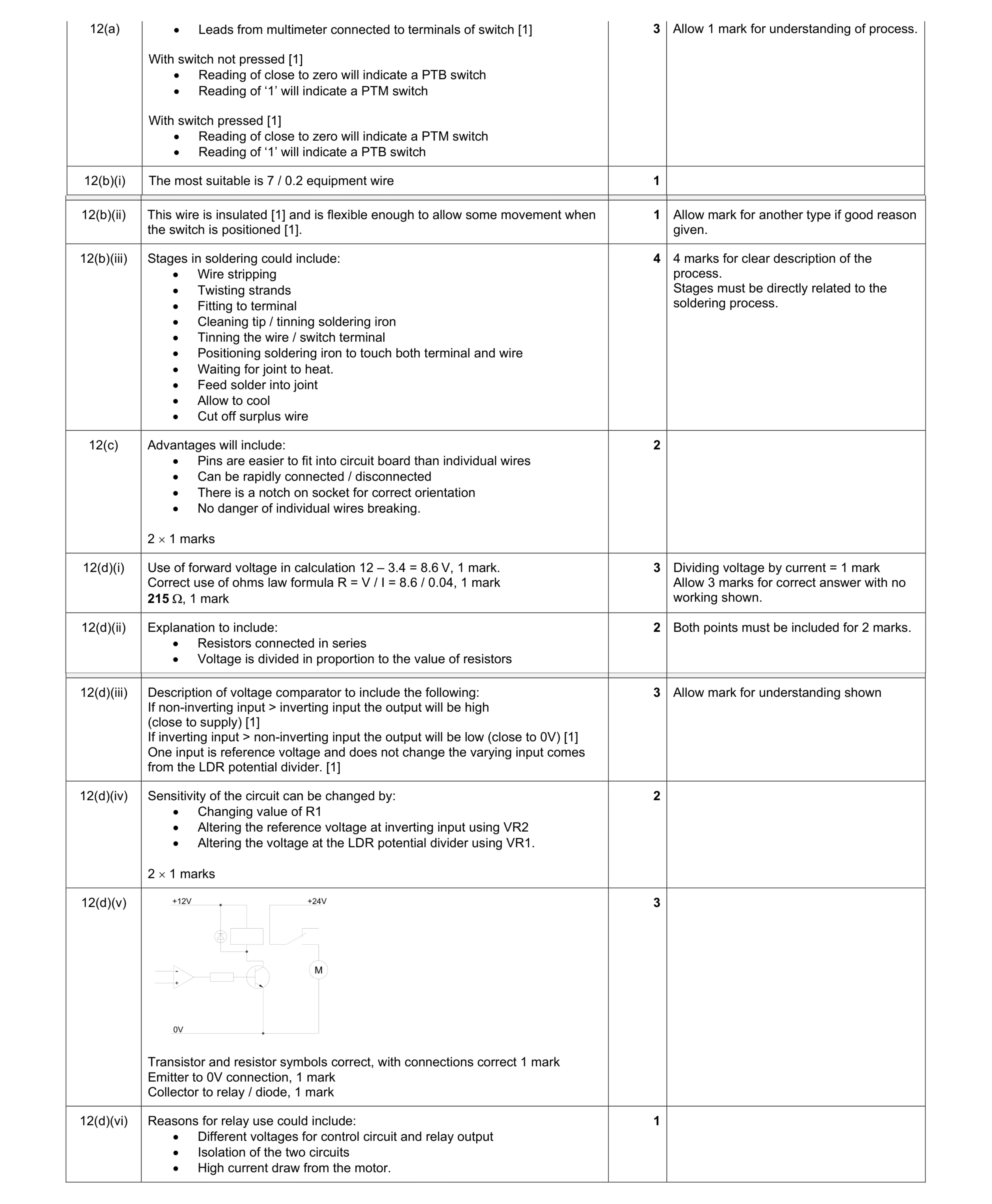 14
14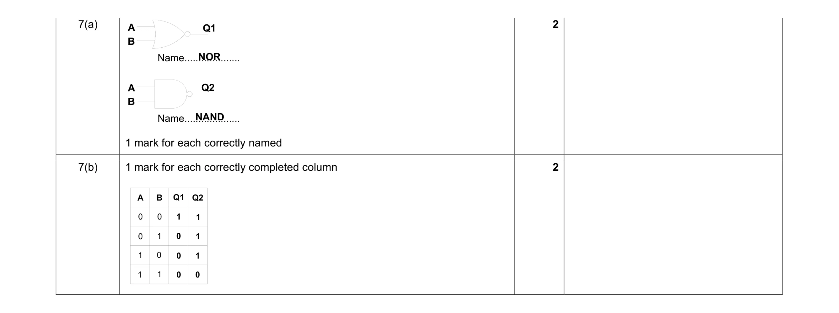 4
4 3
3 1
1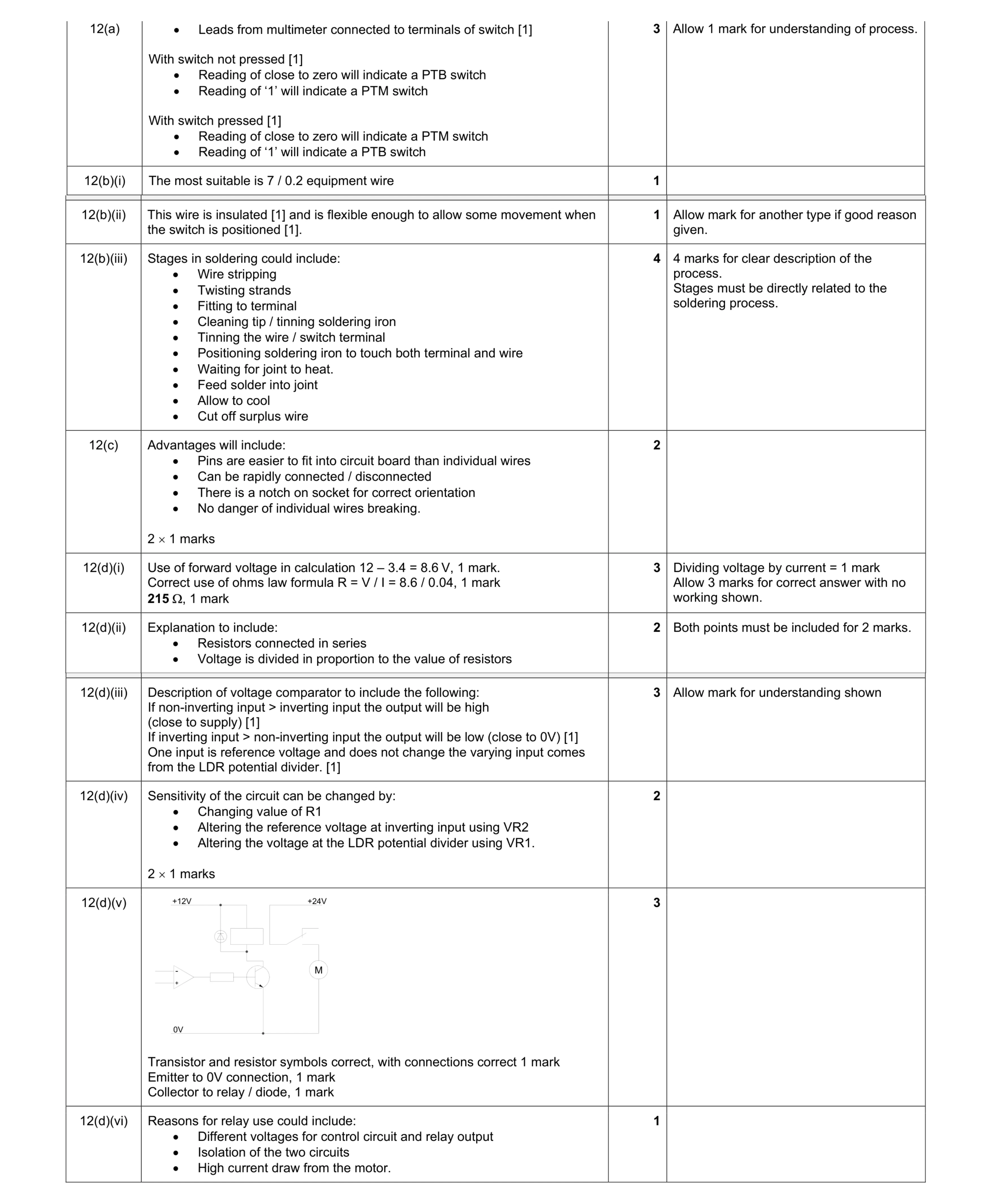 14
14 2
2 3
3 3
3 2
2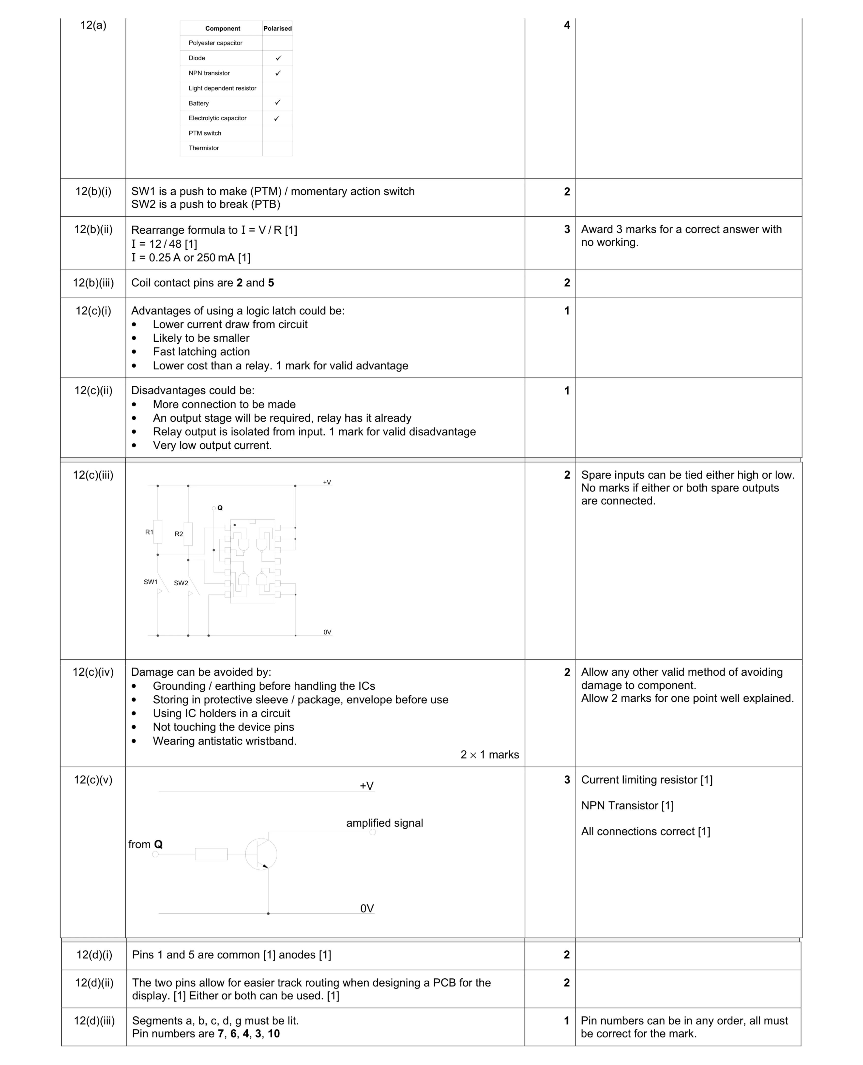 17
17 2
2 3
3 3
3 2
2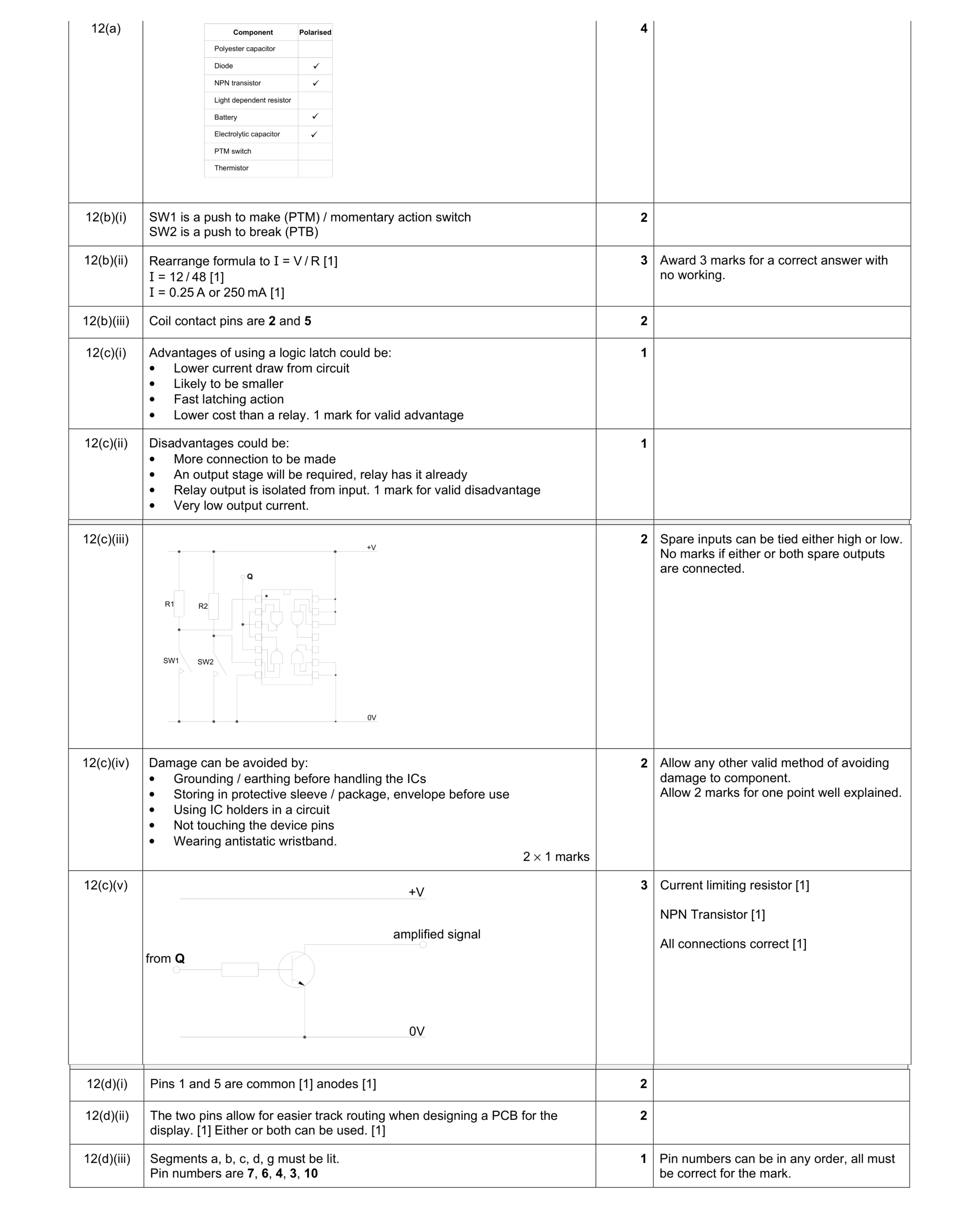 17
17 2
2 3
3 3
3 2
2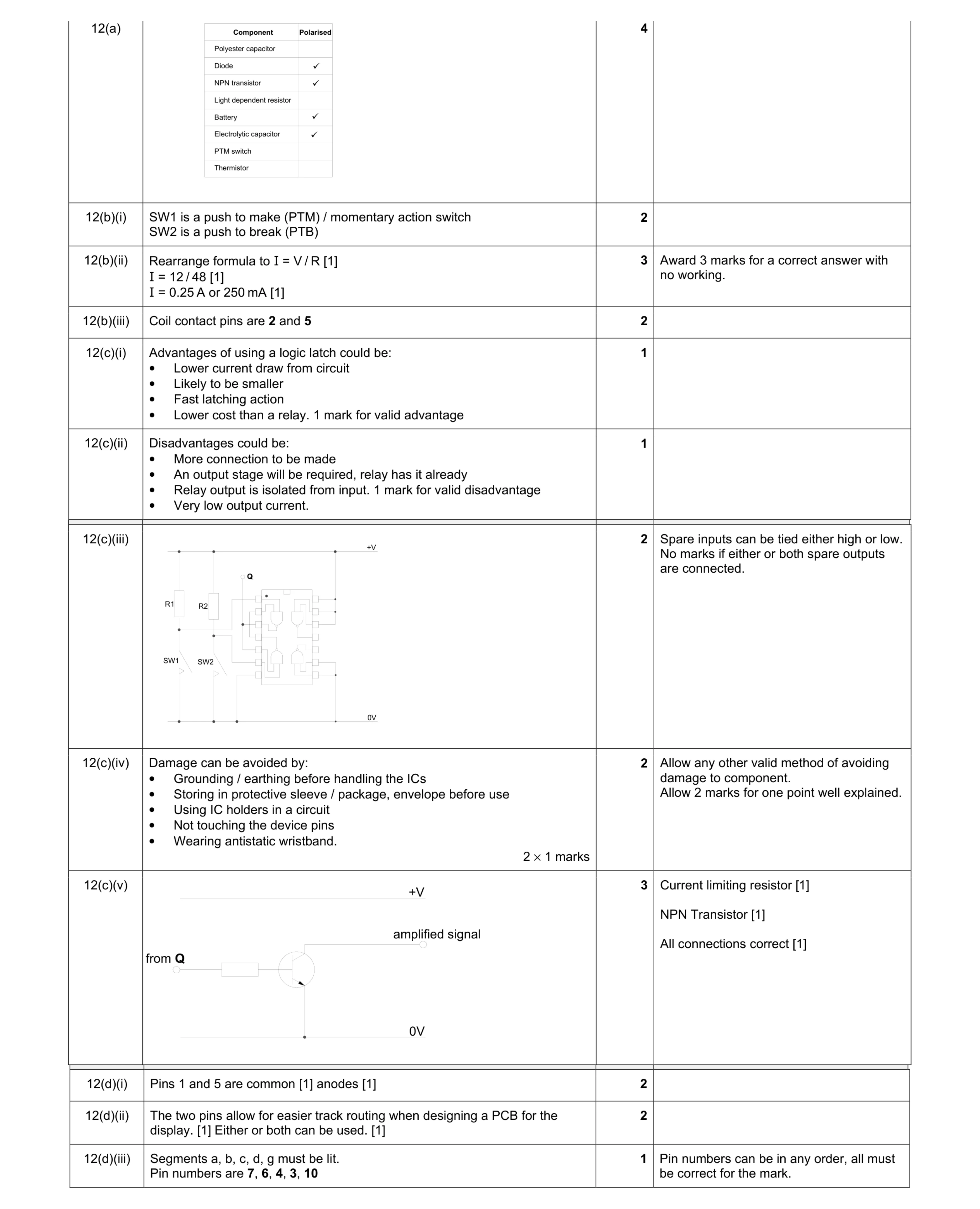 17
17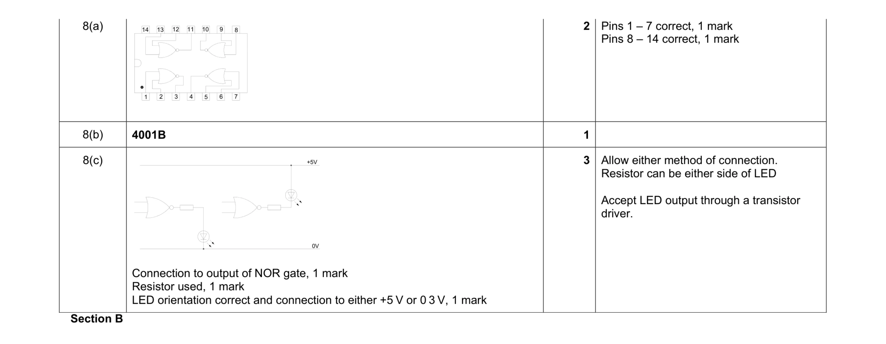 6
6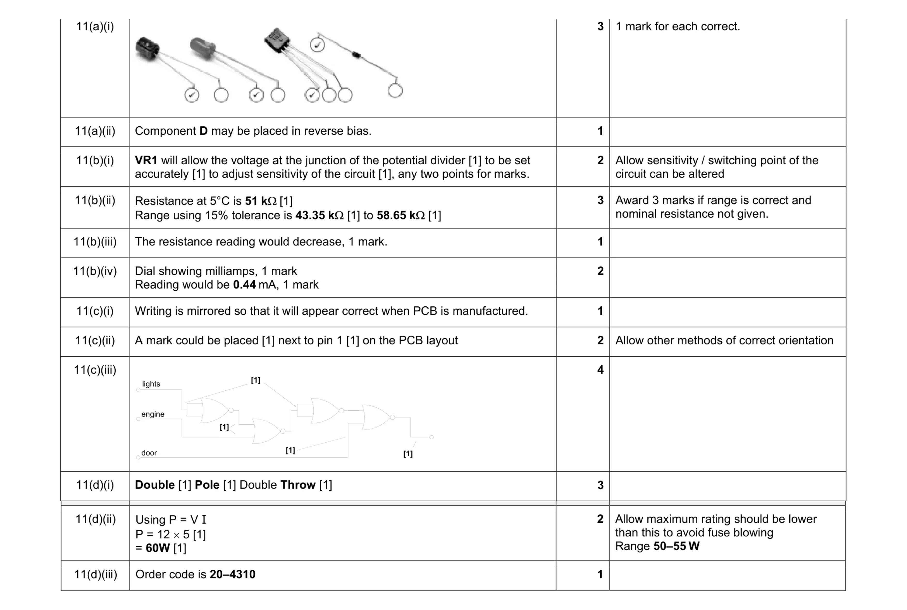 19
19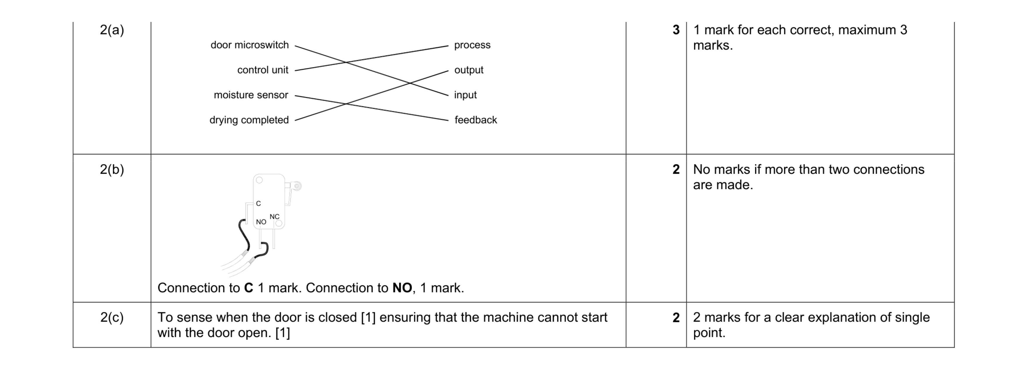 7
7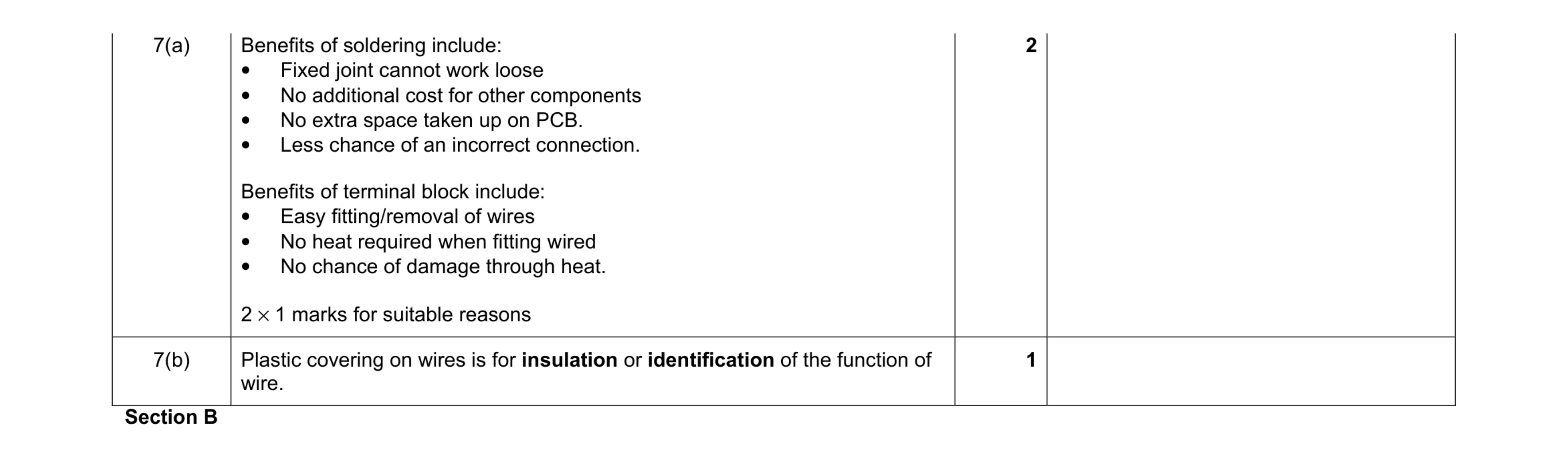 3
3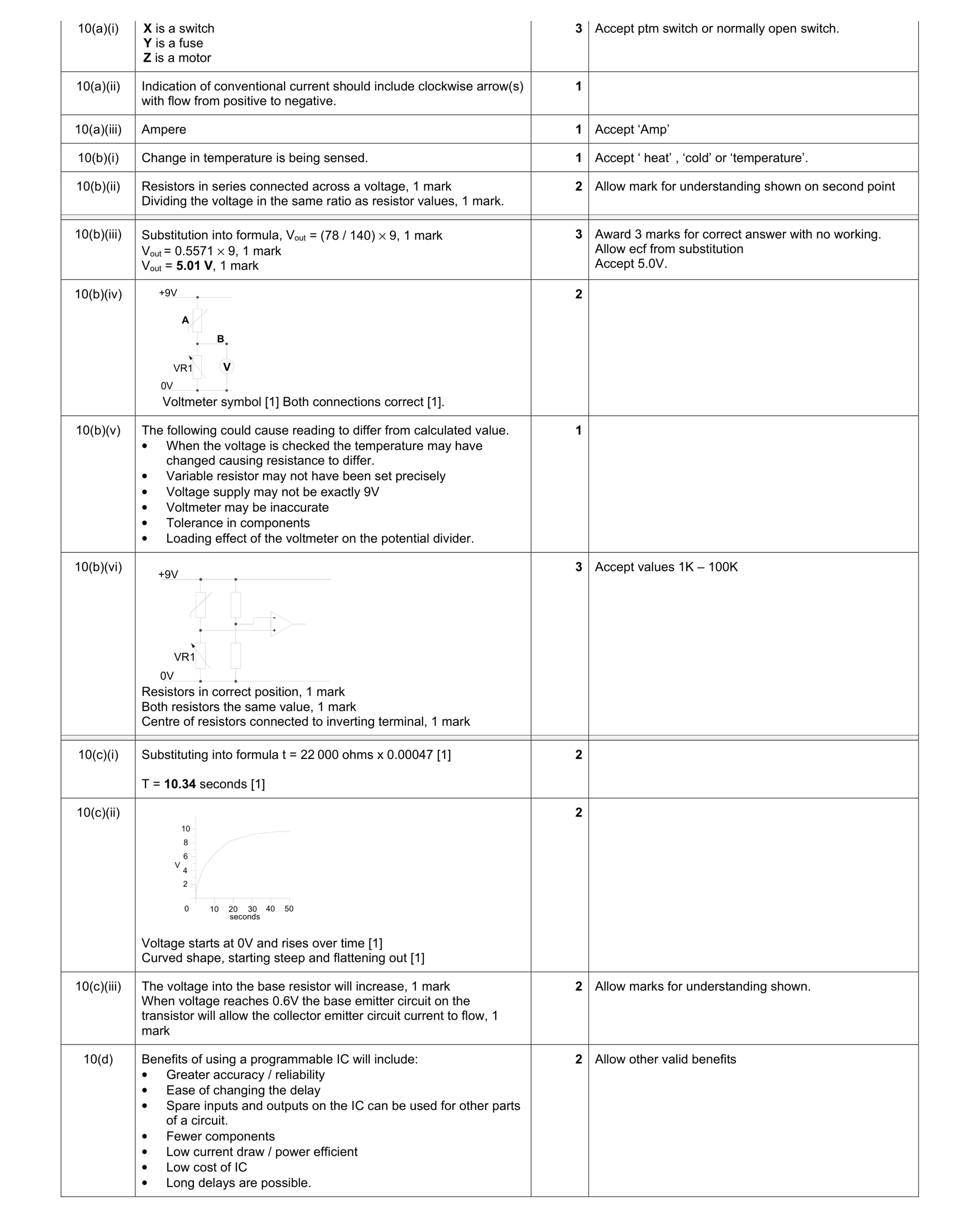 25
25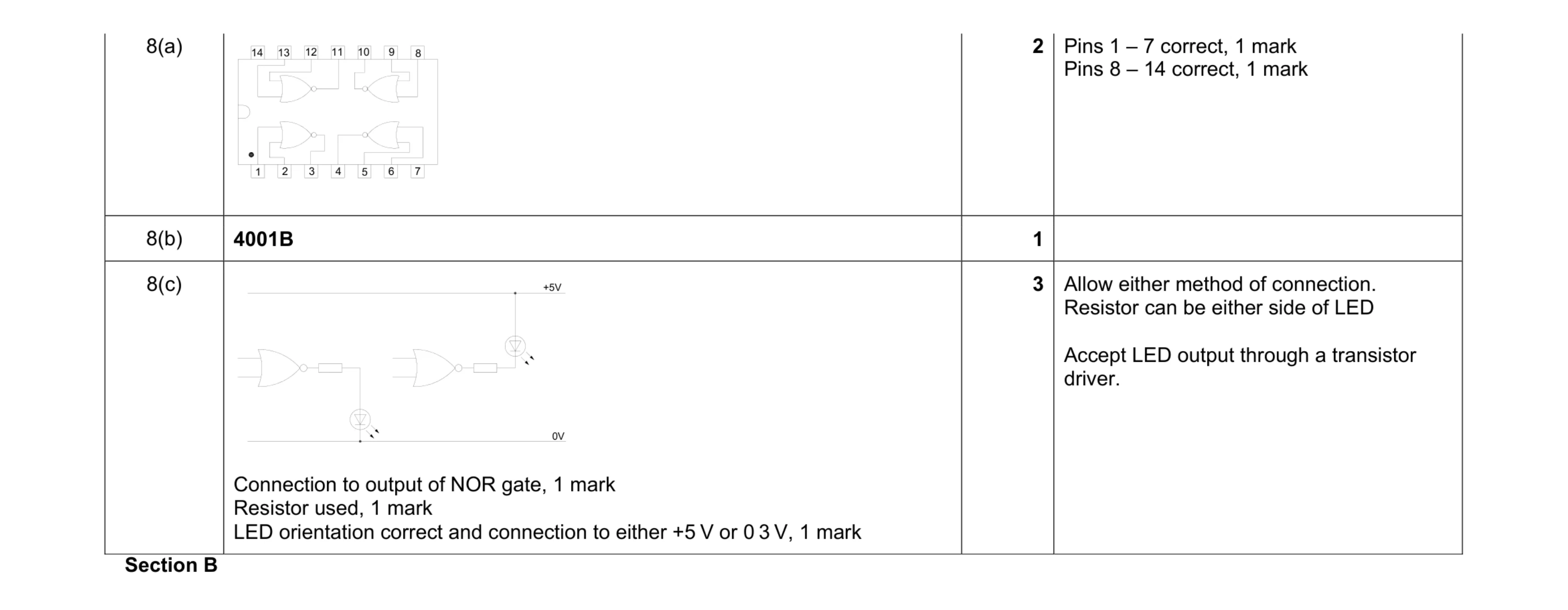 6
6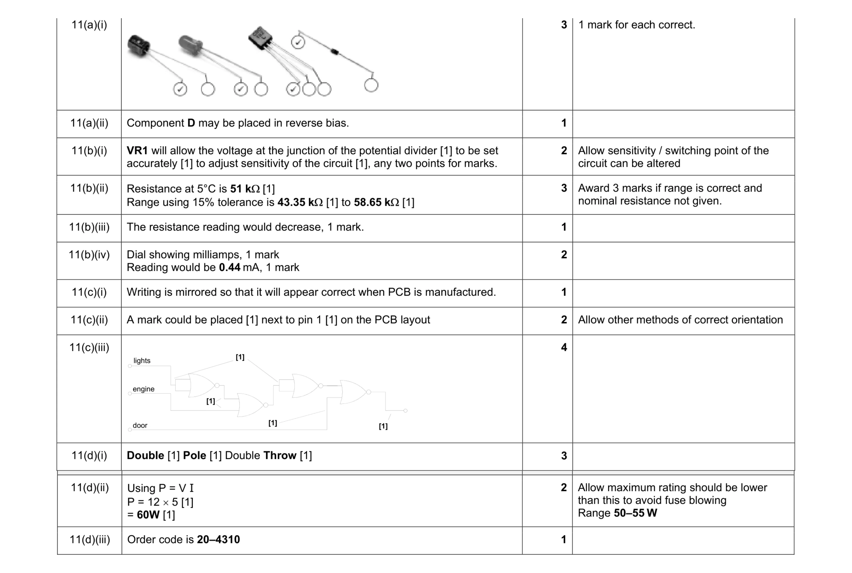 19
19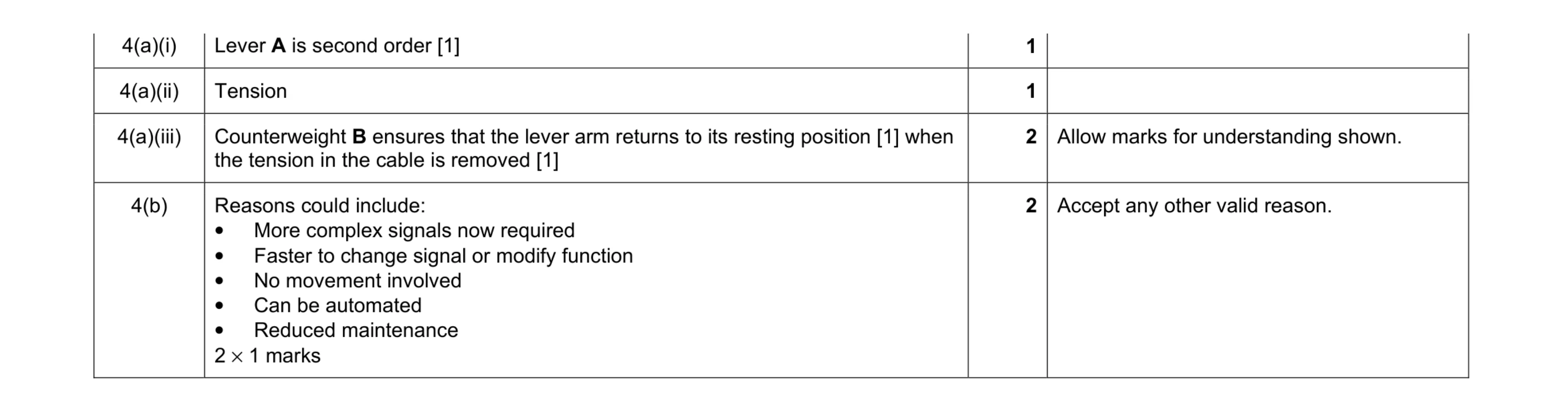 6
6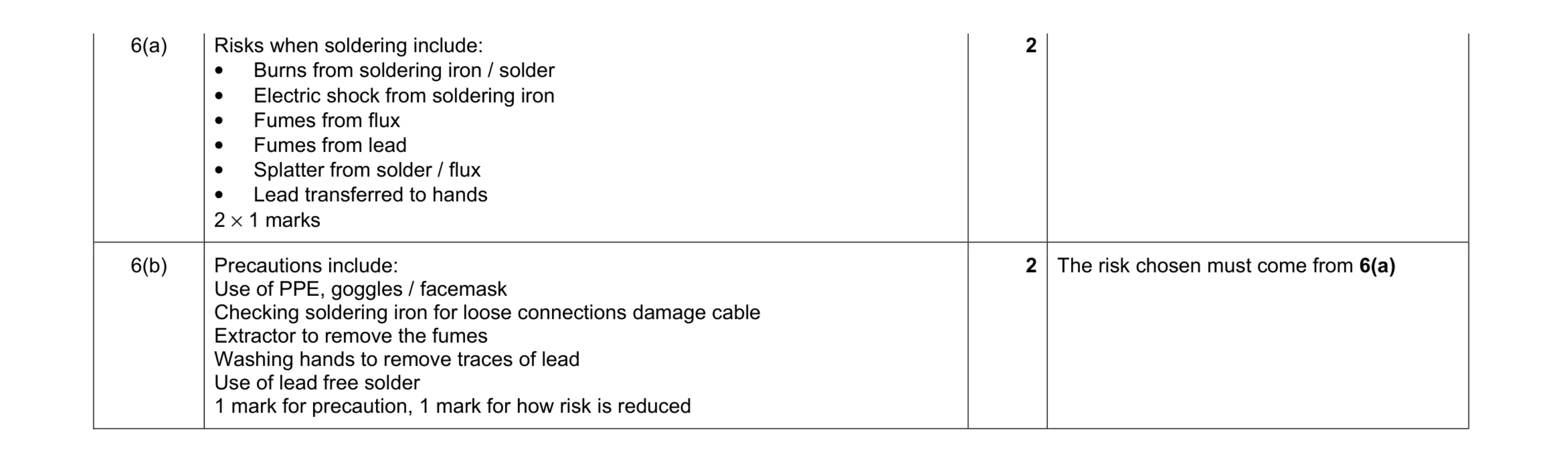 4
4 1
1 3
3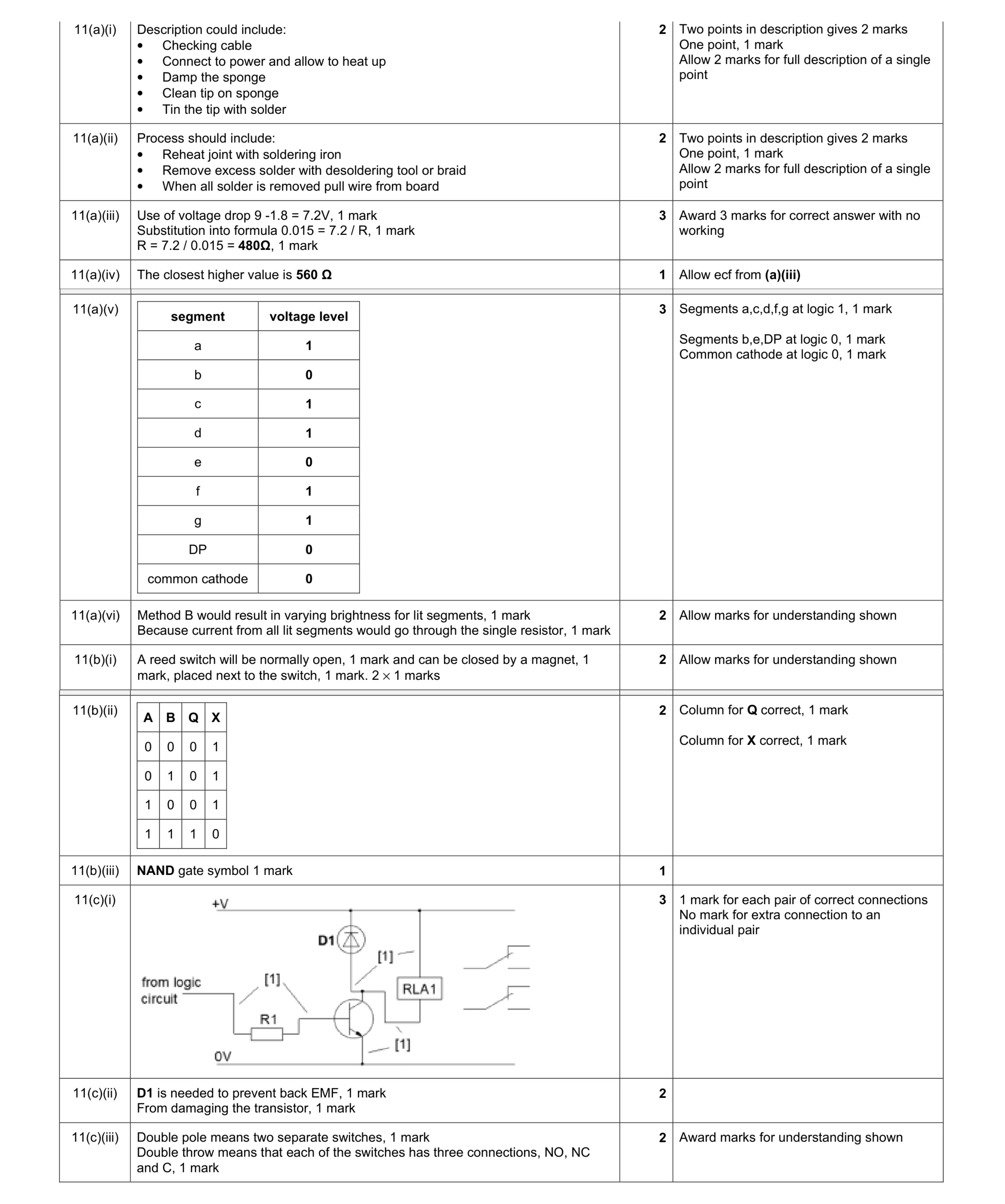 21
21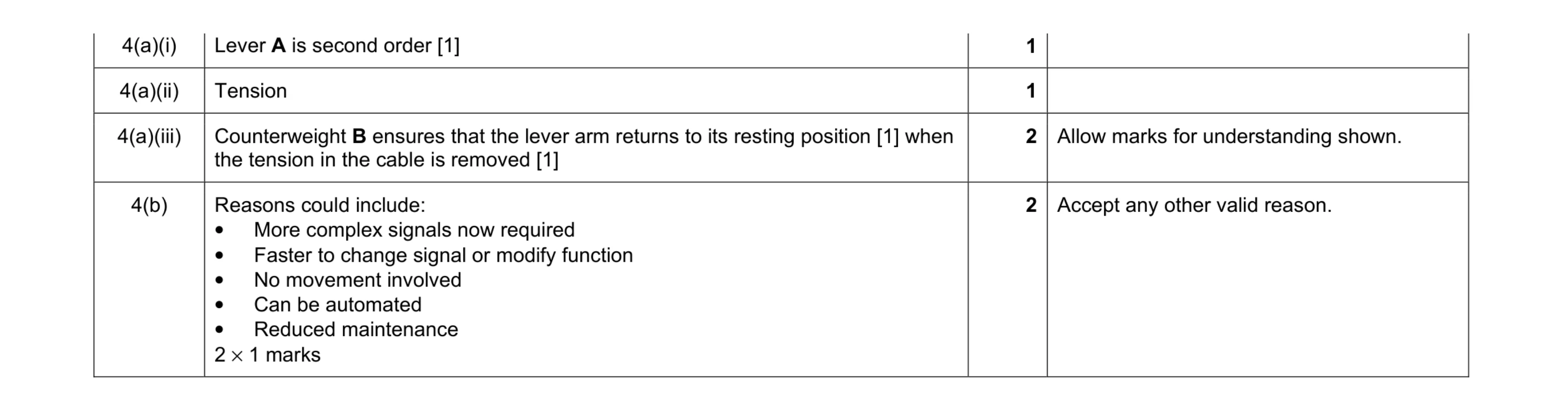 6
6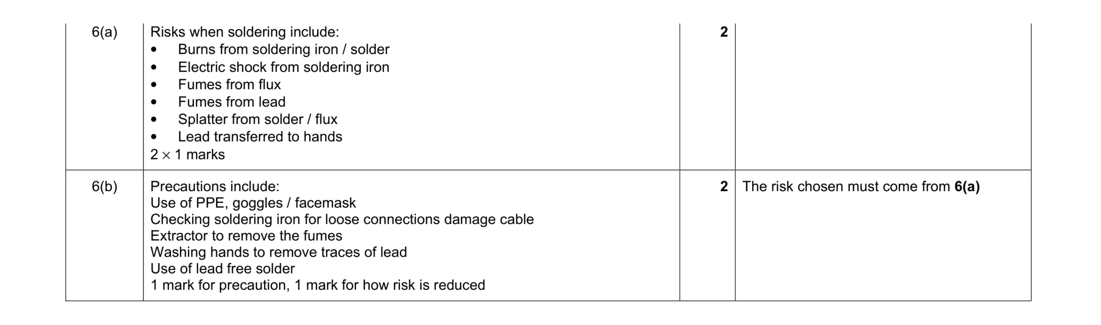 4
4 1
1 3
3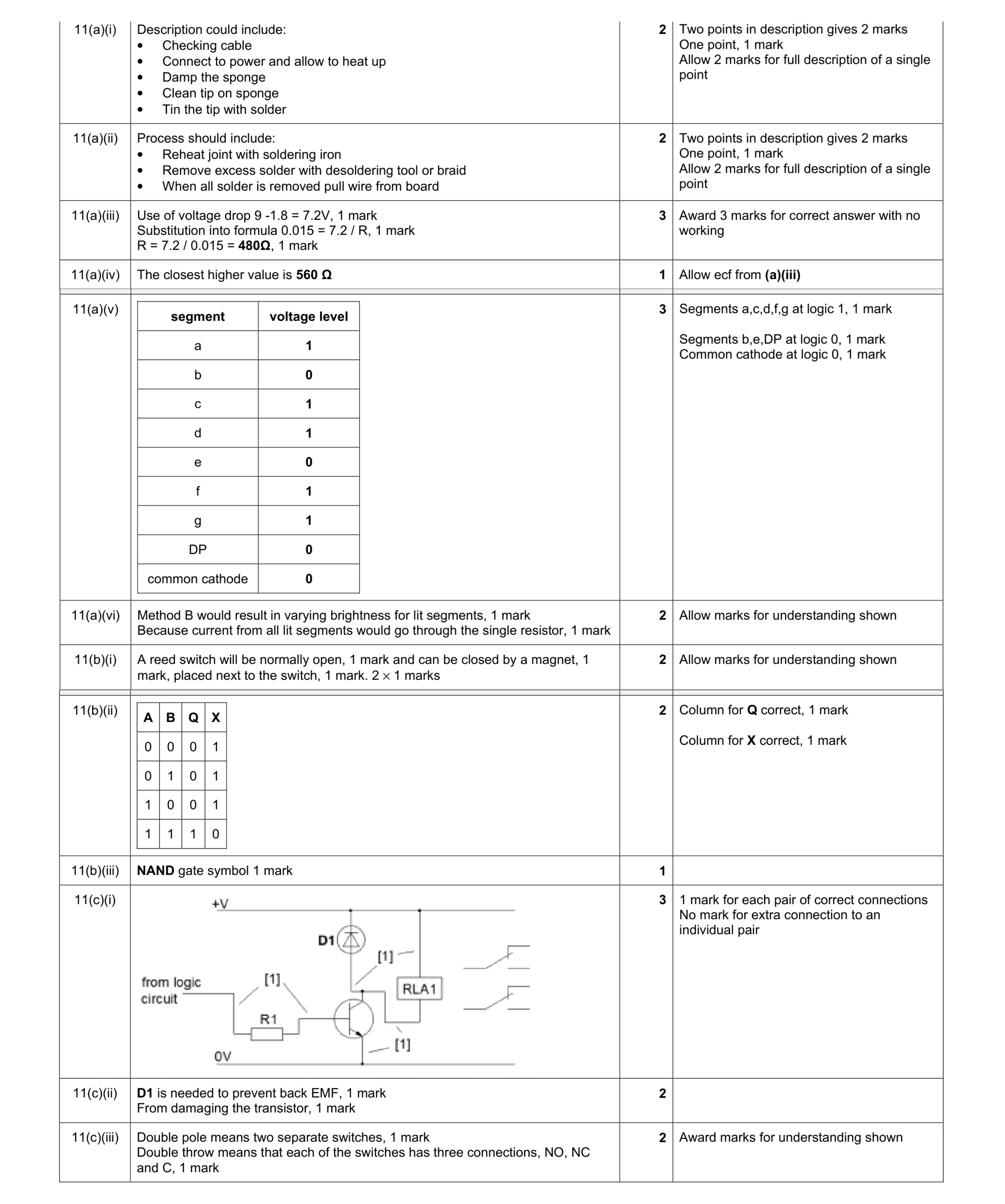 21
21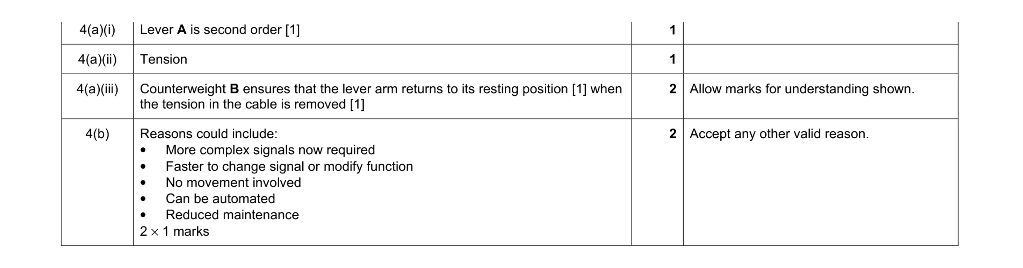 6
6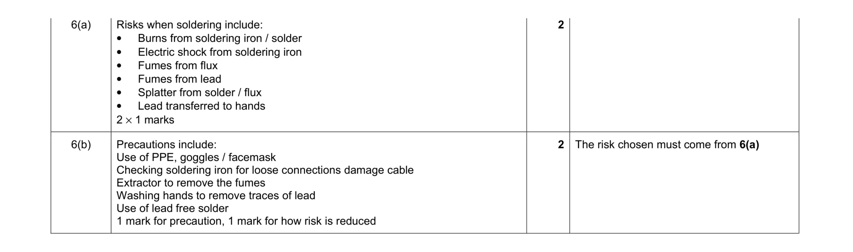 4
4 1
1 3
3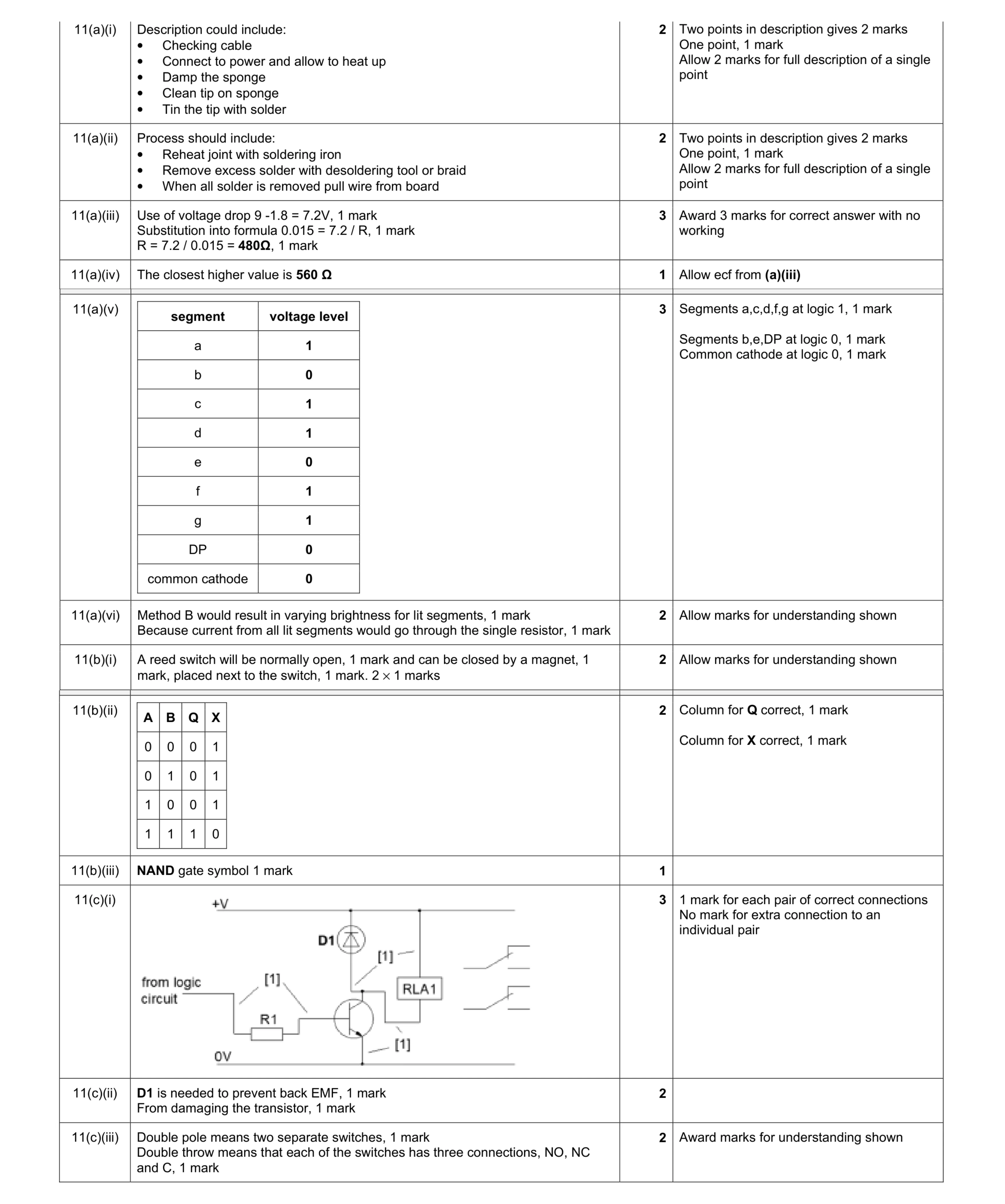 21
21 2
2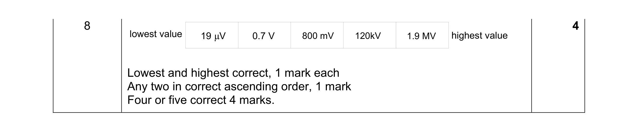 4
4 3
3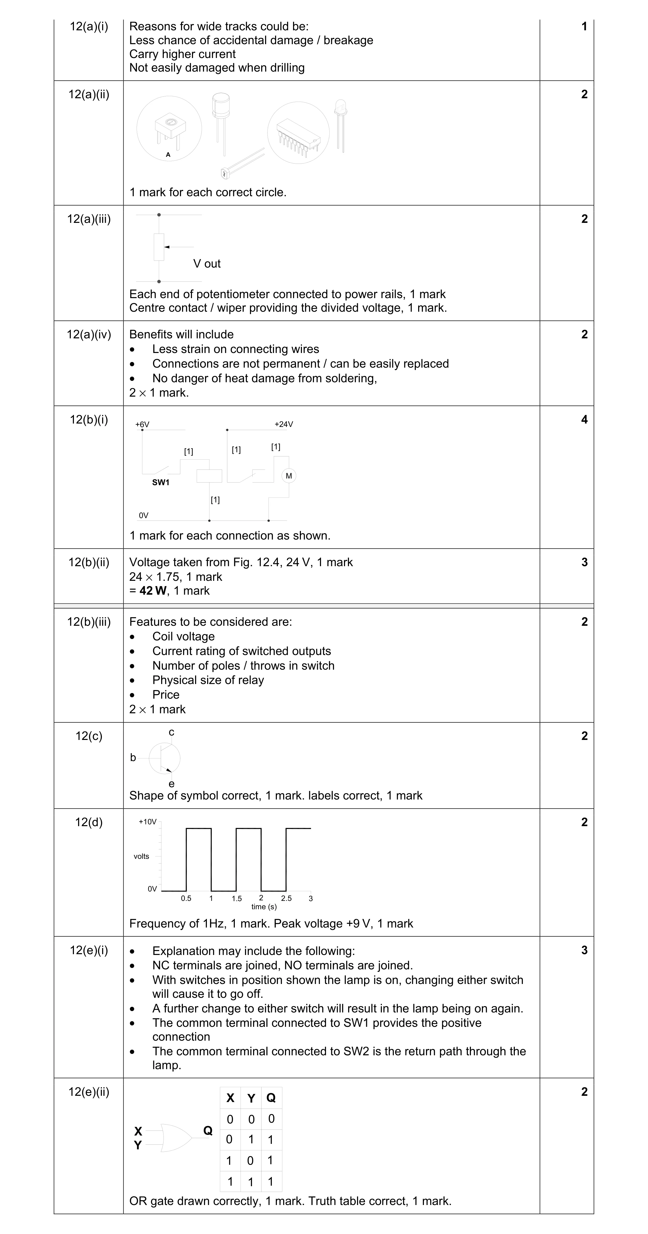 16
16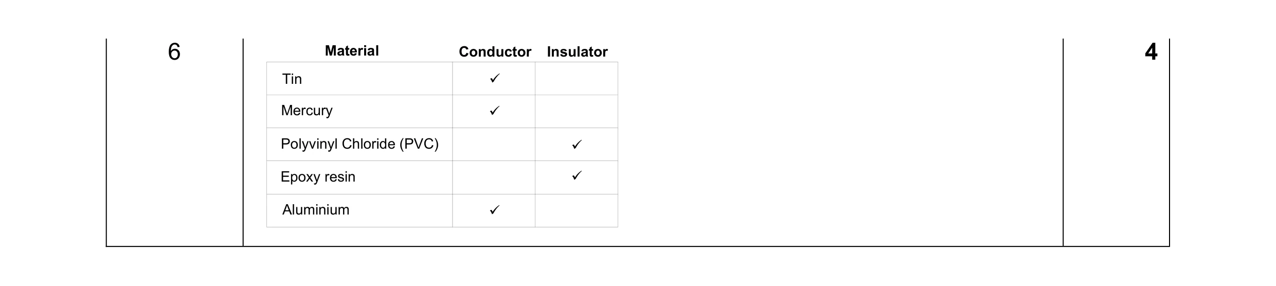 4
4 3
3 2
2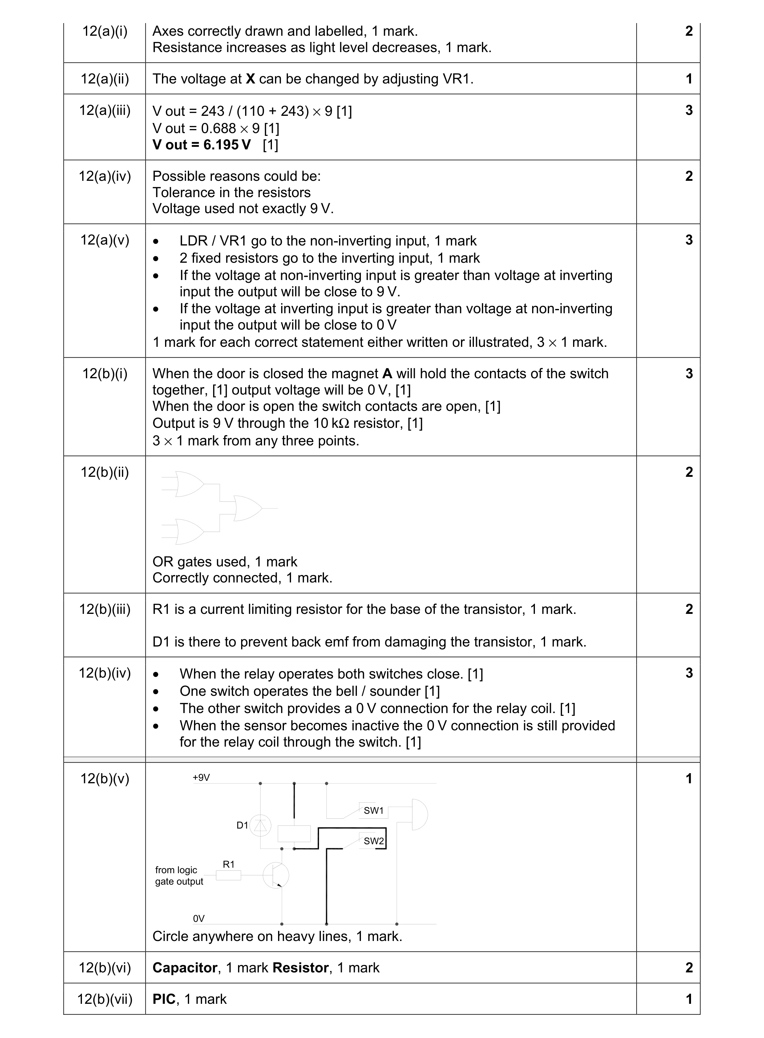 11
11 2
2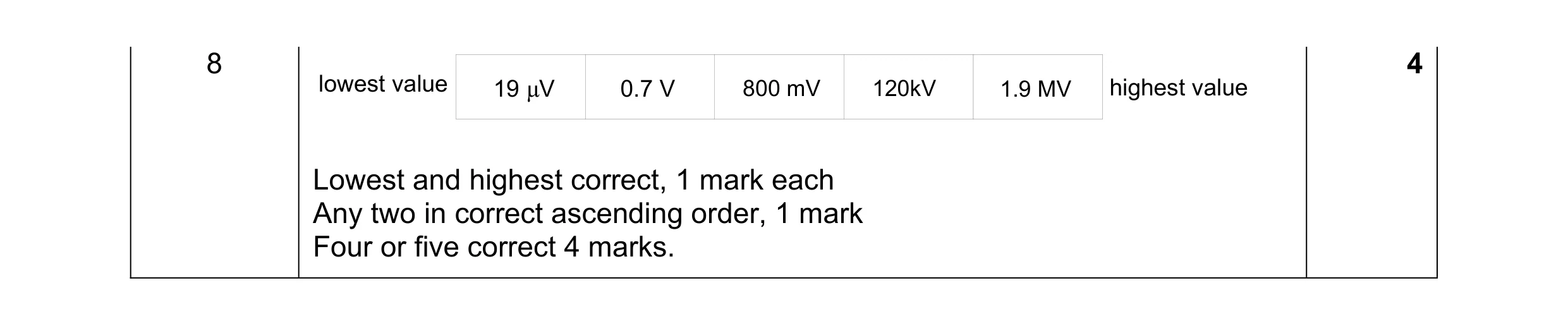 4
4 3
3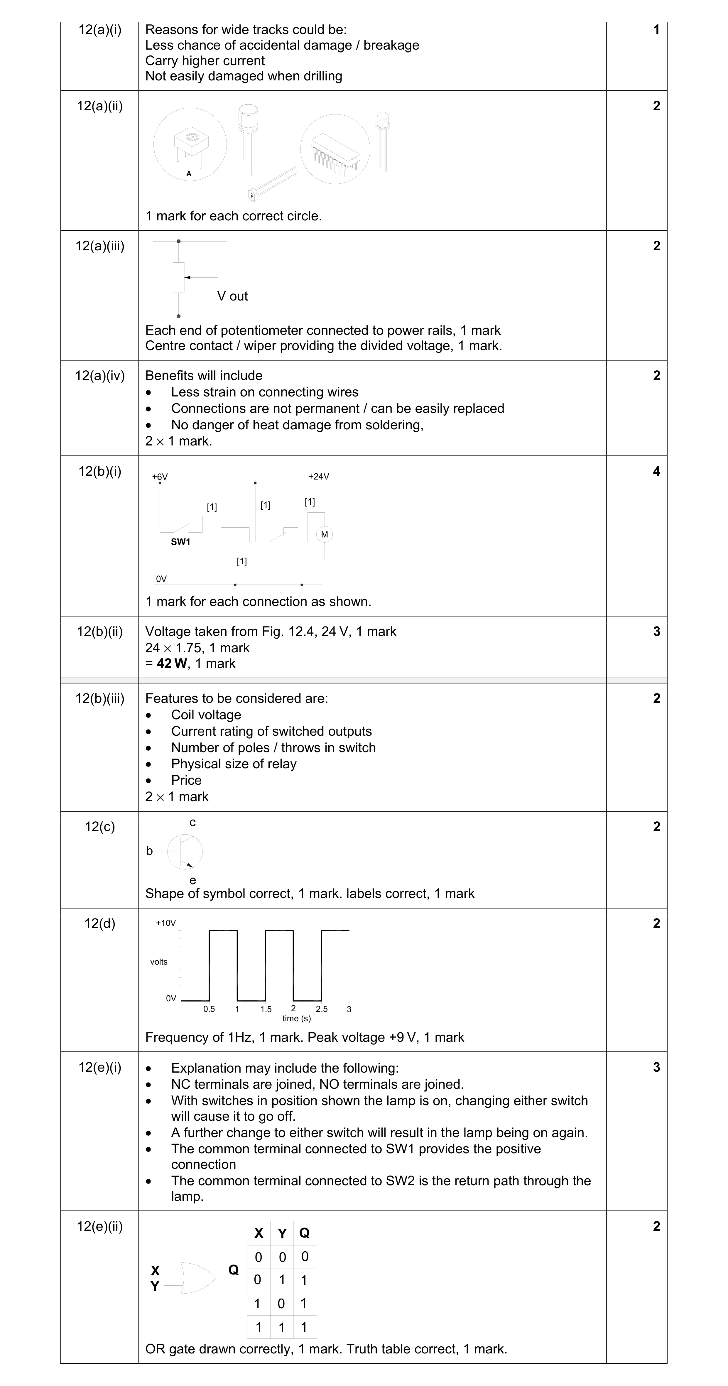 16
16 3
3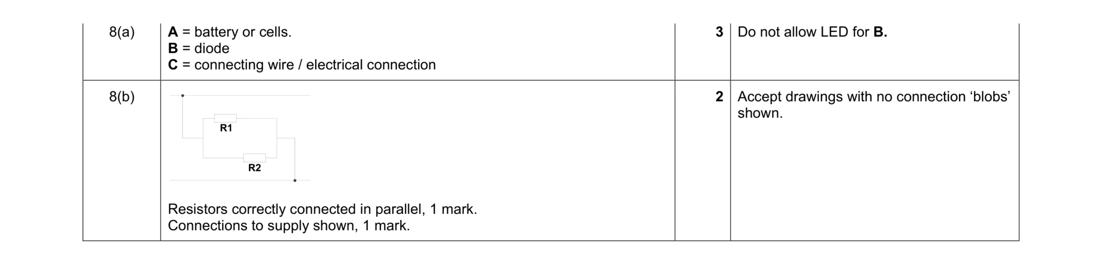 5
5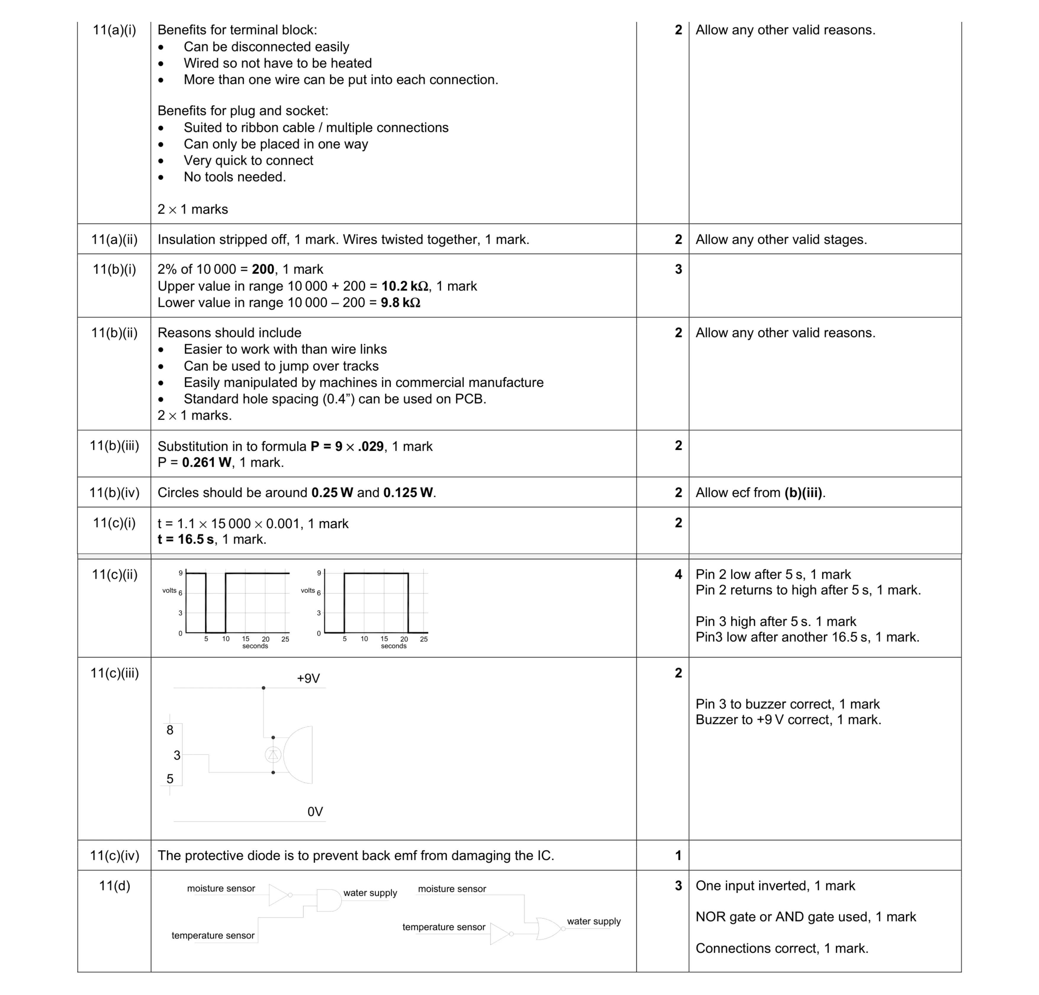 19
19 3
3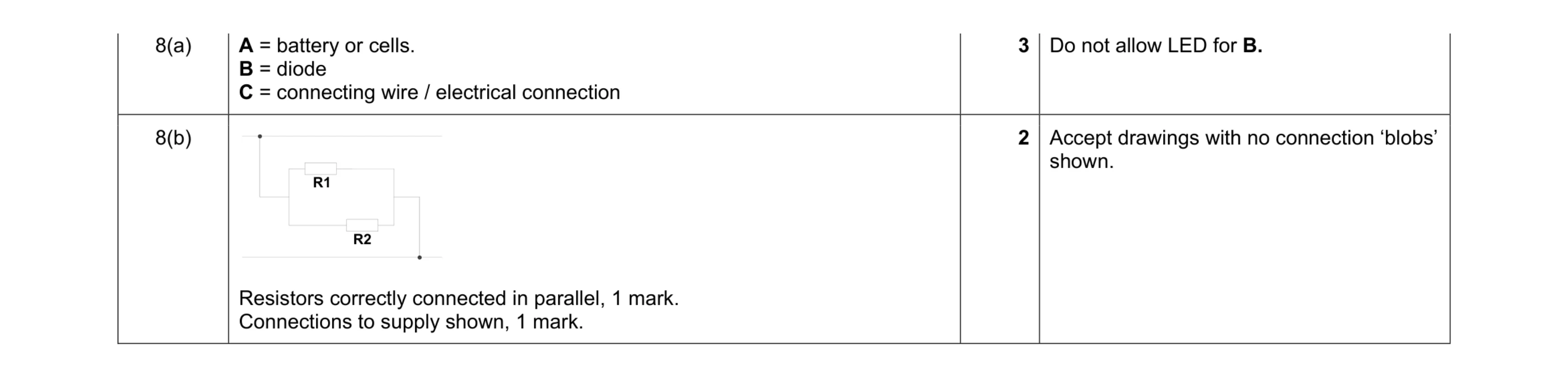 5
5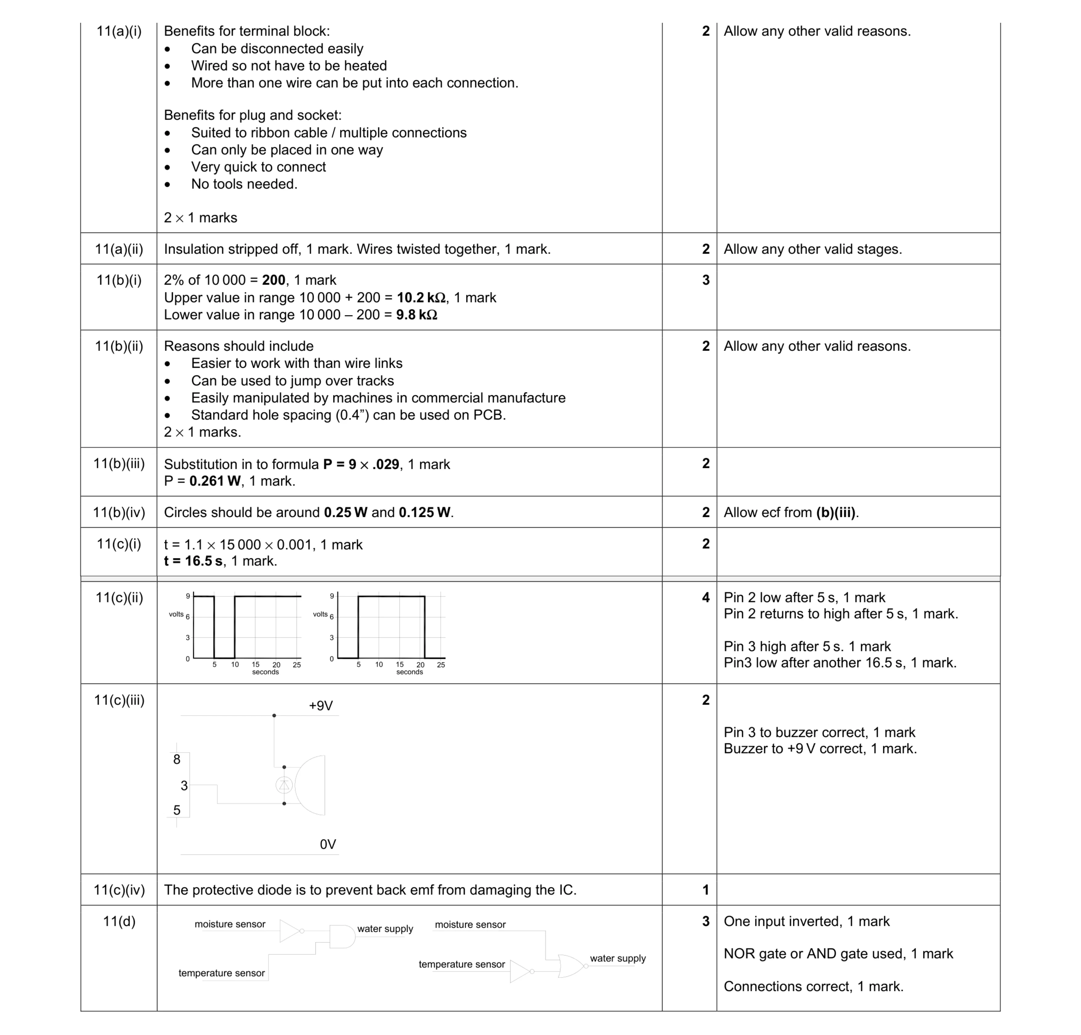 19
19 3
3 4
4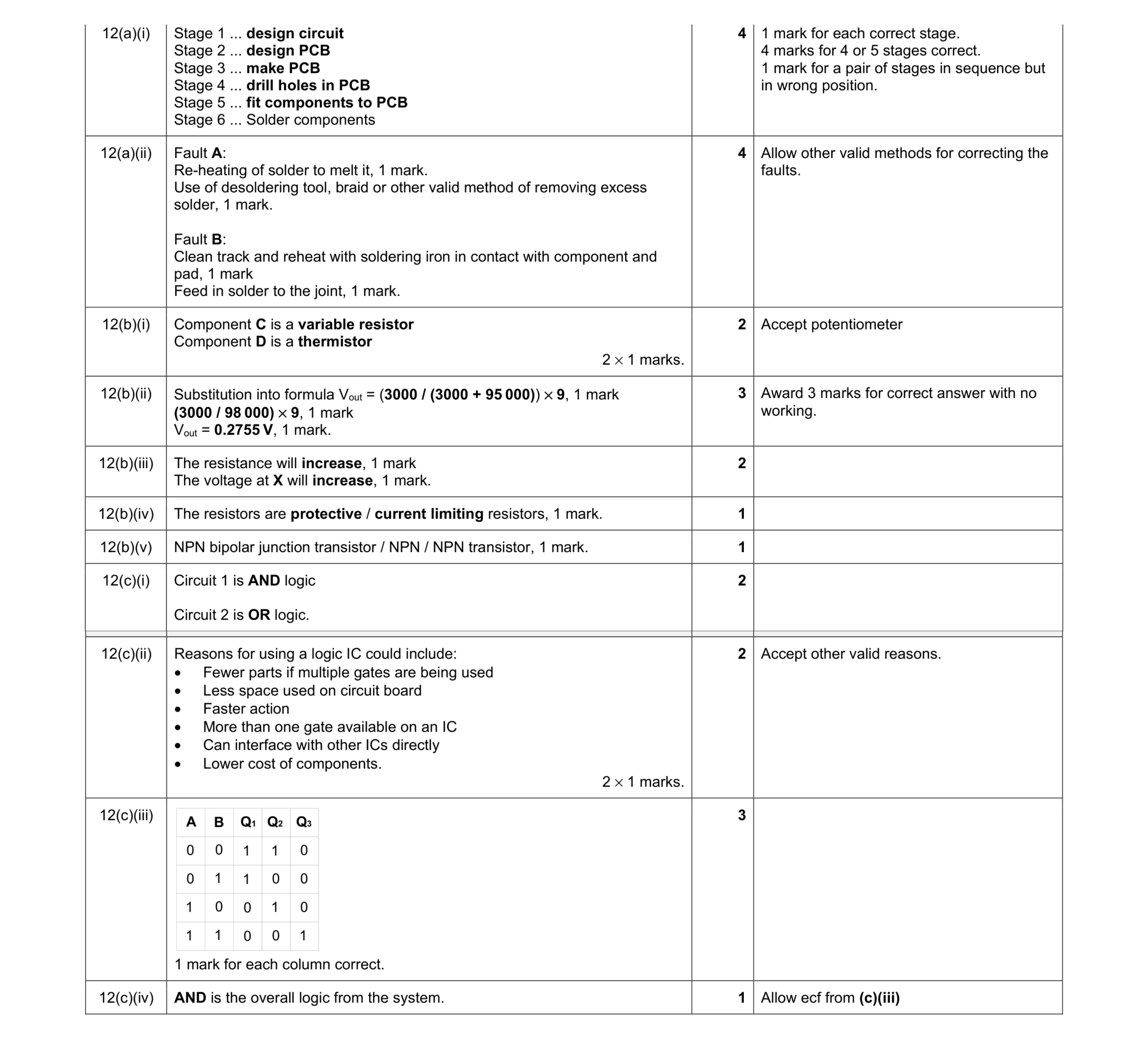 19
19 3
3 2
2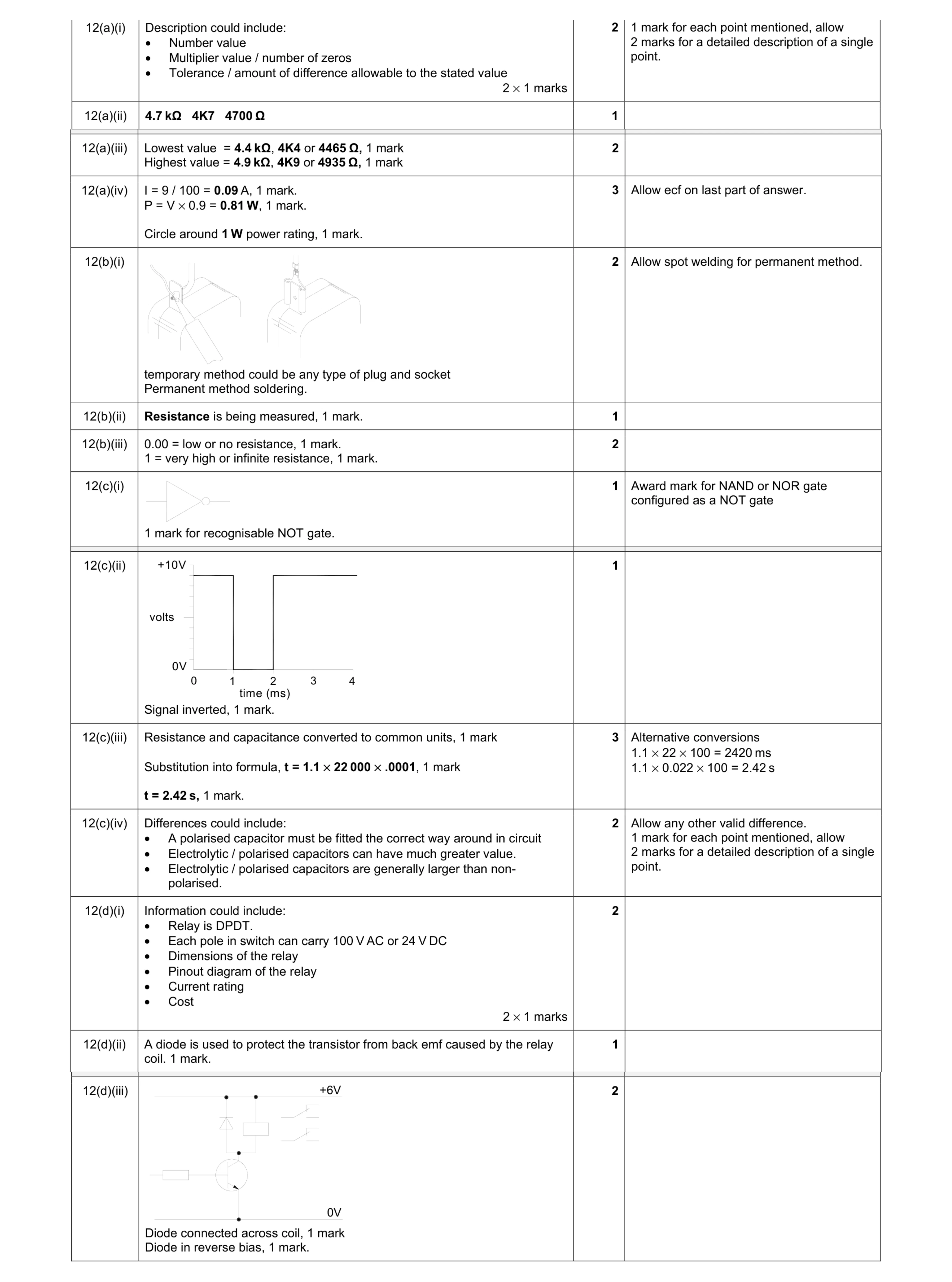 14
14 5
5 2
2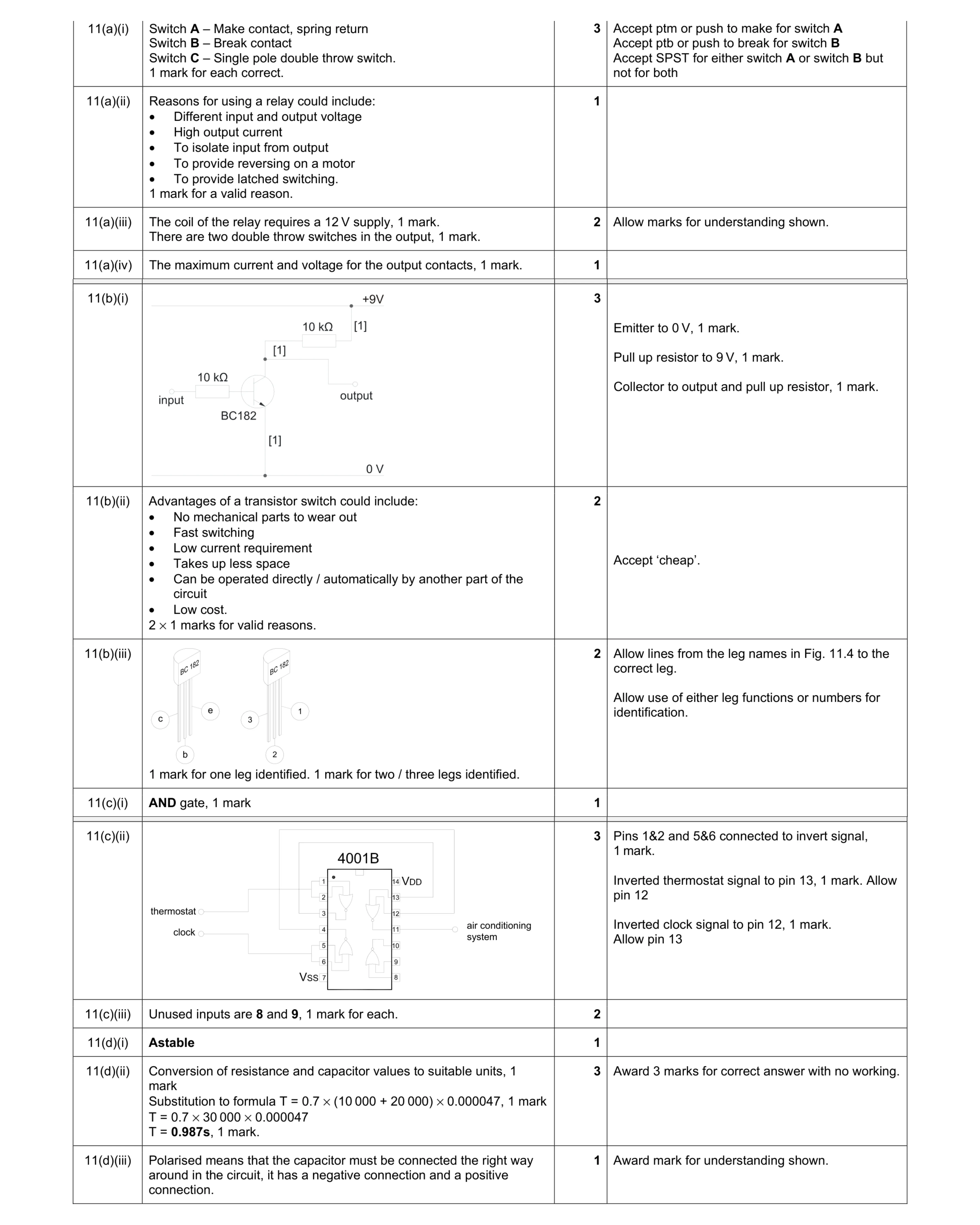 20
20 3
3 2
2 1
1 2
2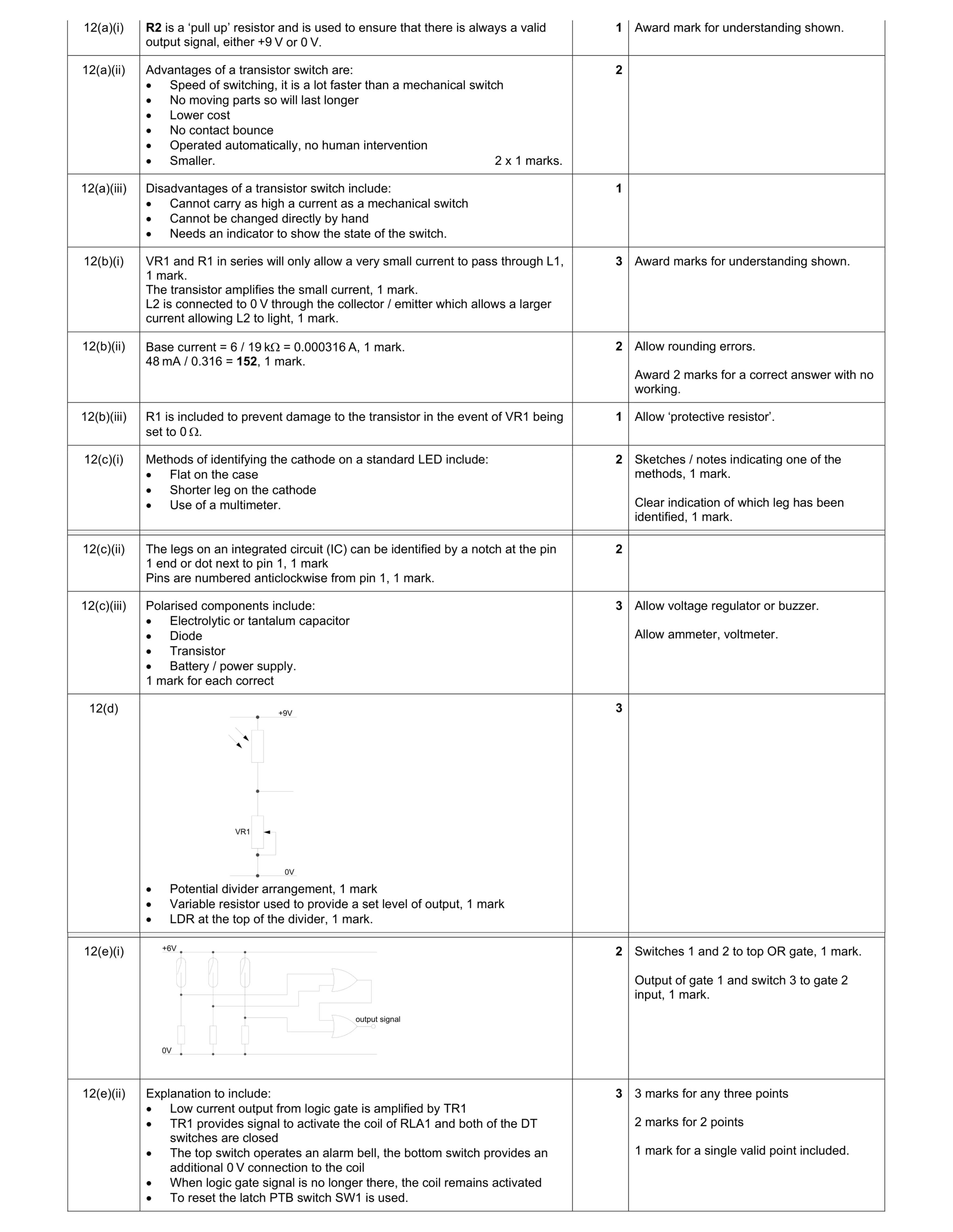 17
17 1
1 4
4 2
2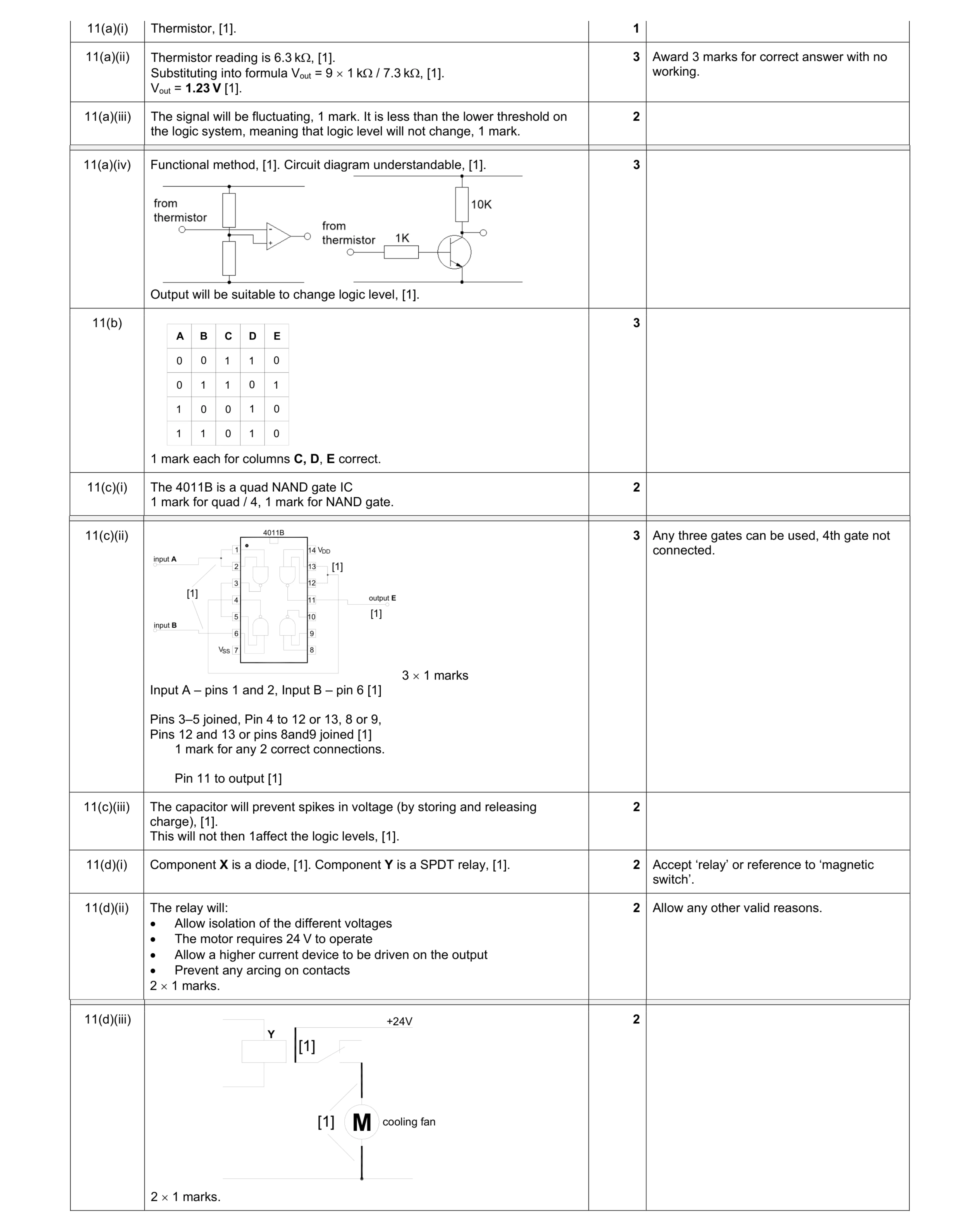 19
19 3
3 2
2 1
1 2
2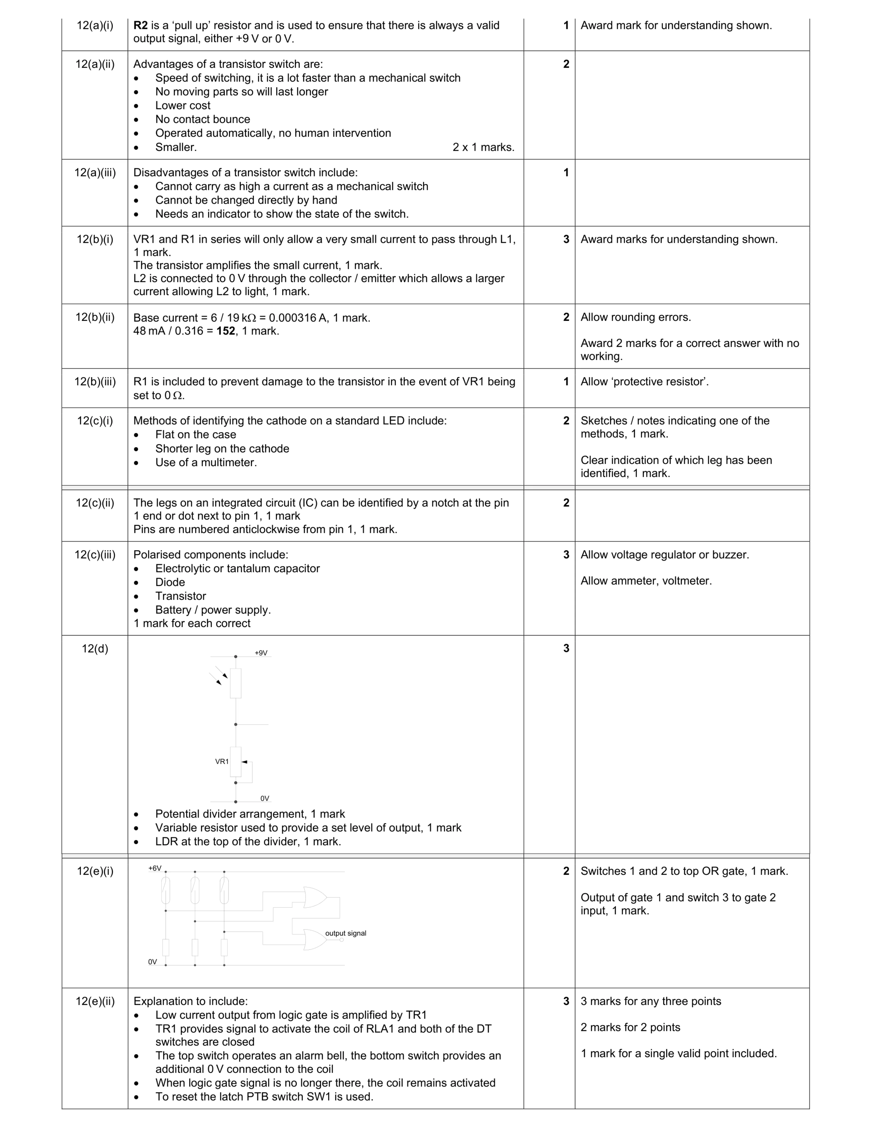 17
17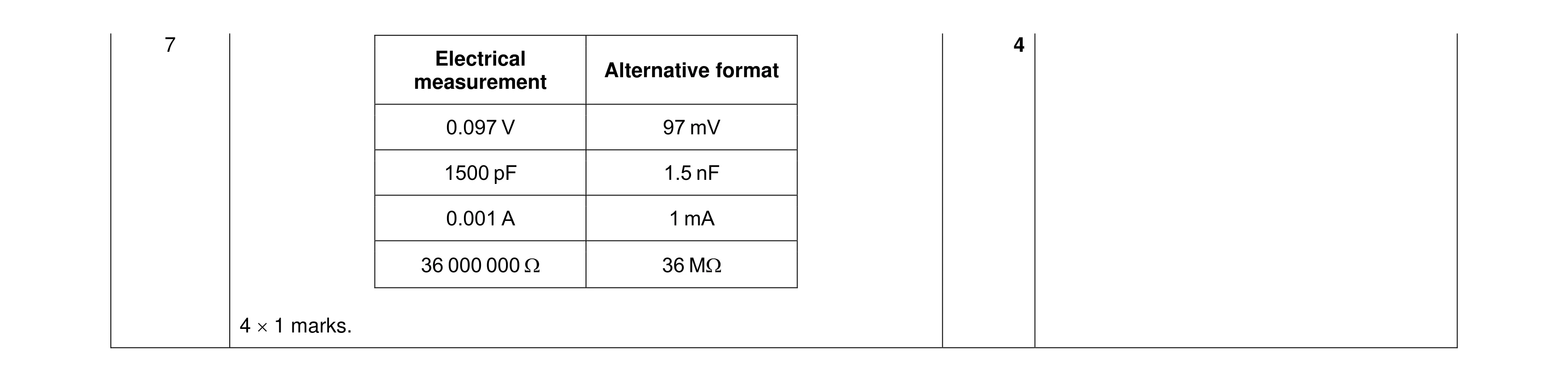 4
4 3
3 2
2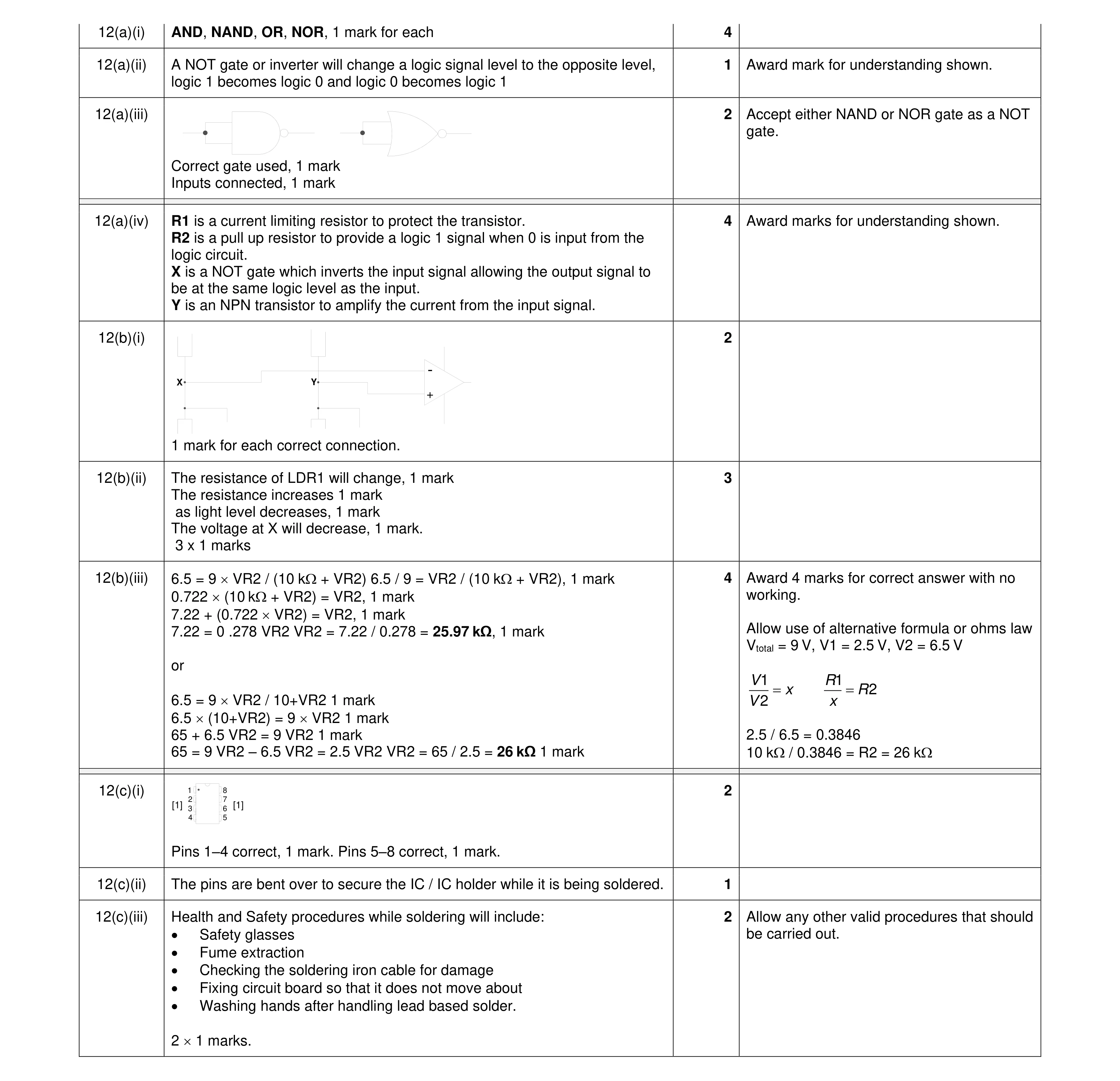 25
25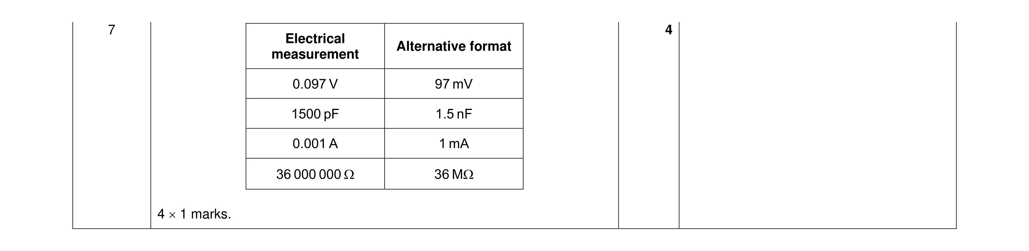 4
4 3
3 2
2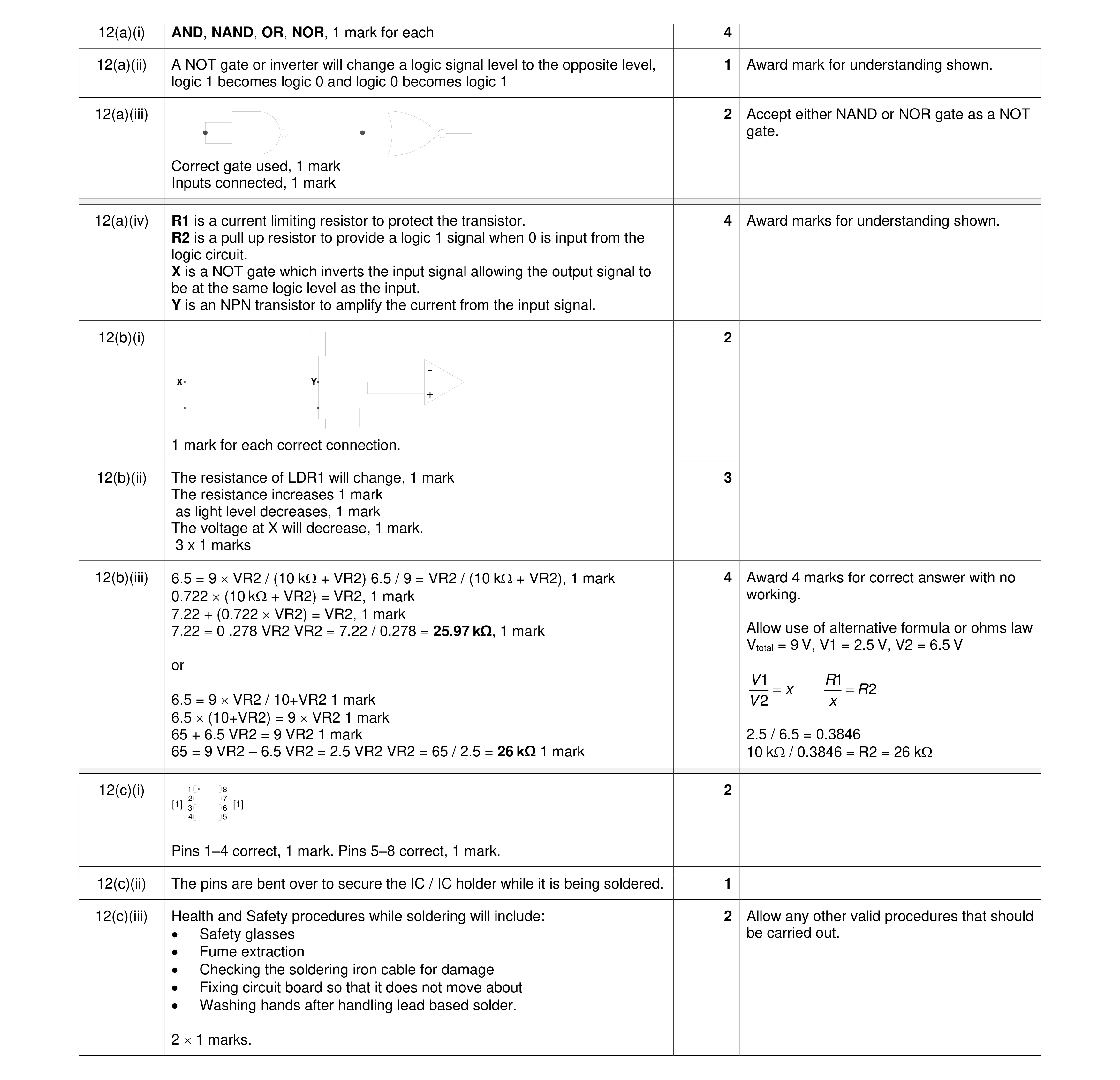 25
25 3
3 2
2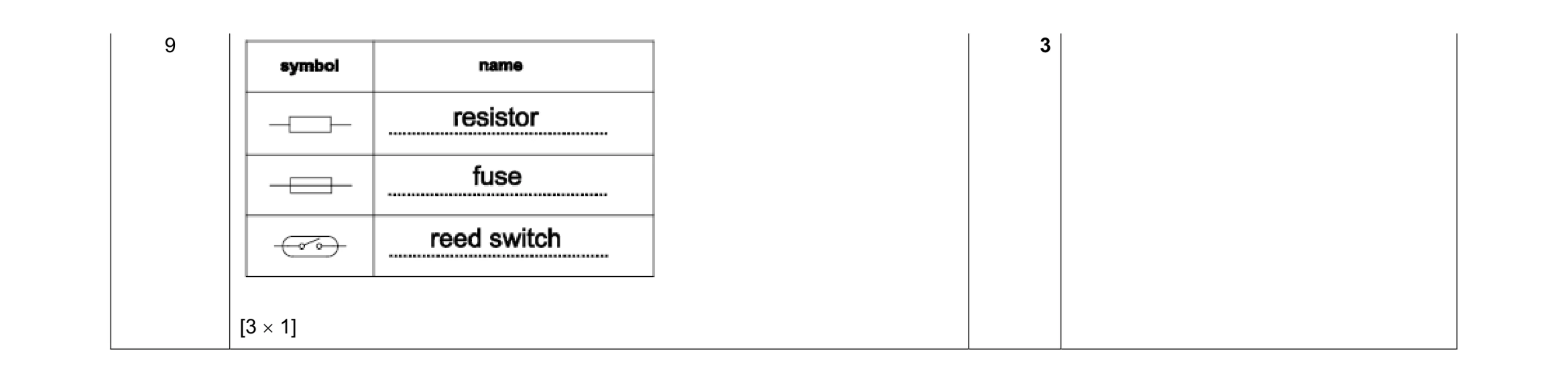 3
3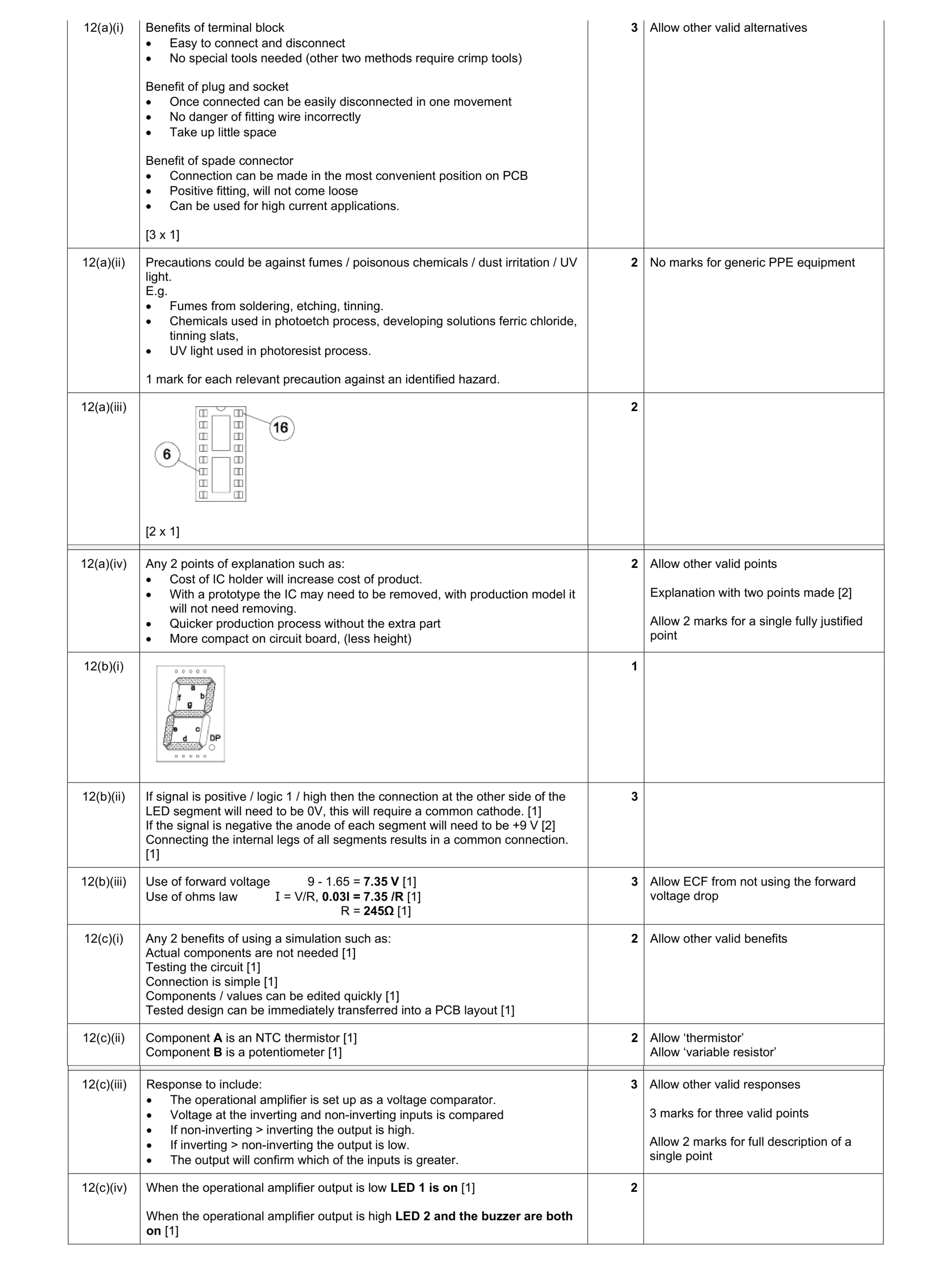 16
16 3
3 4
4 3
3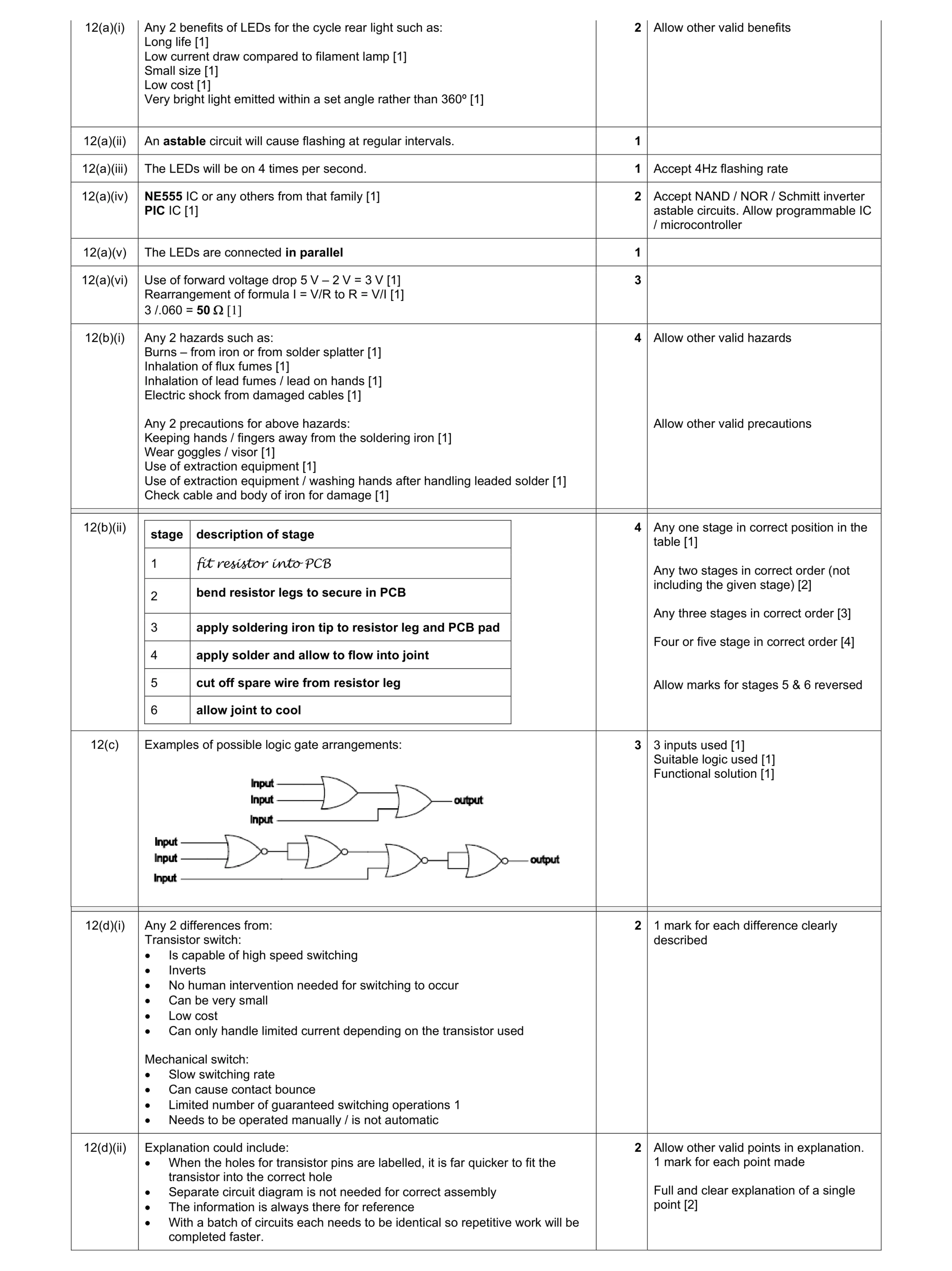 21
21 3
3 2
2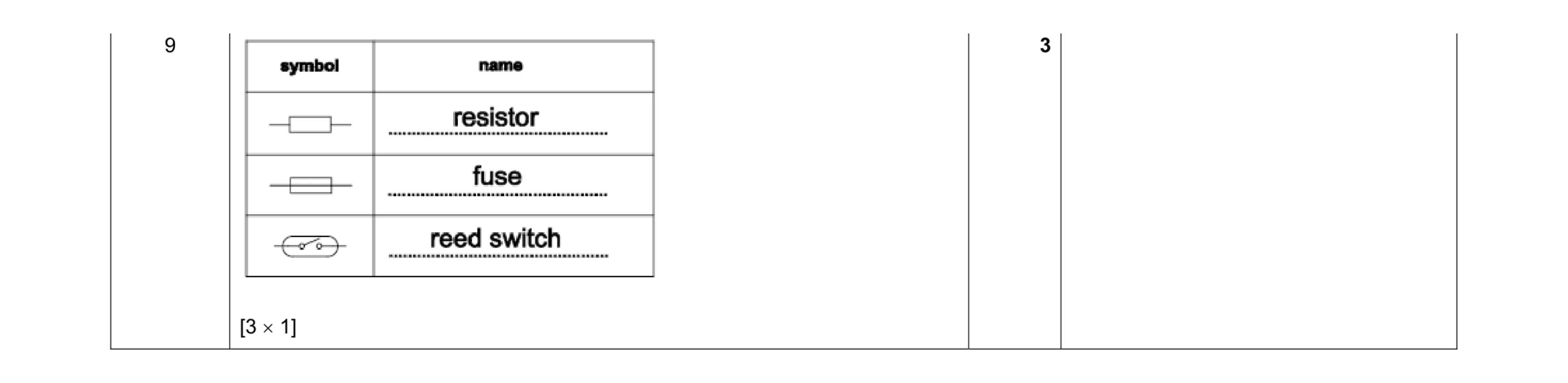 3
3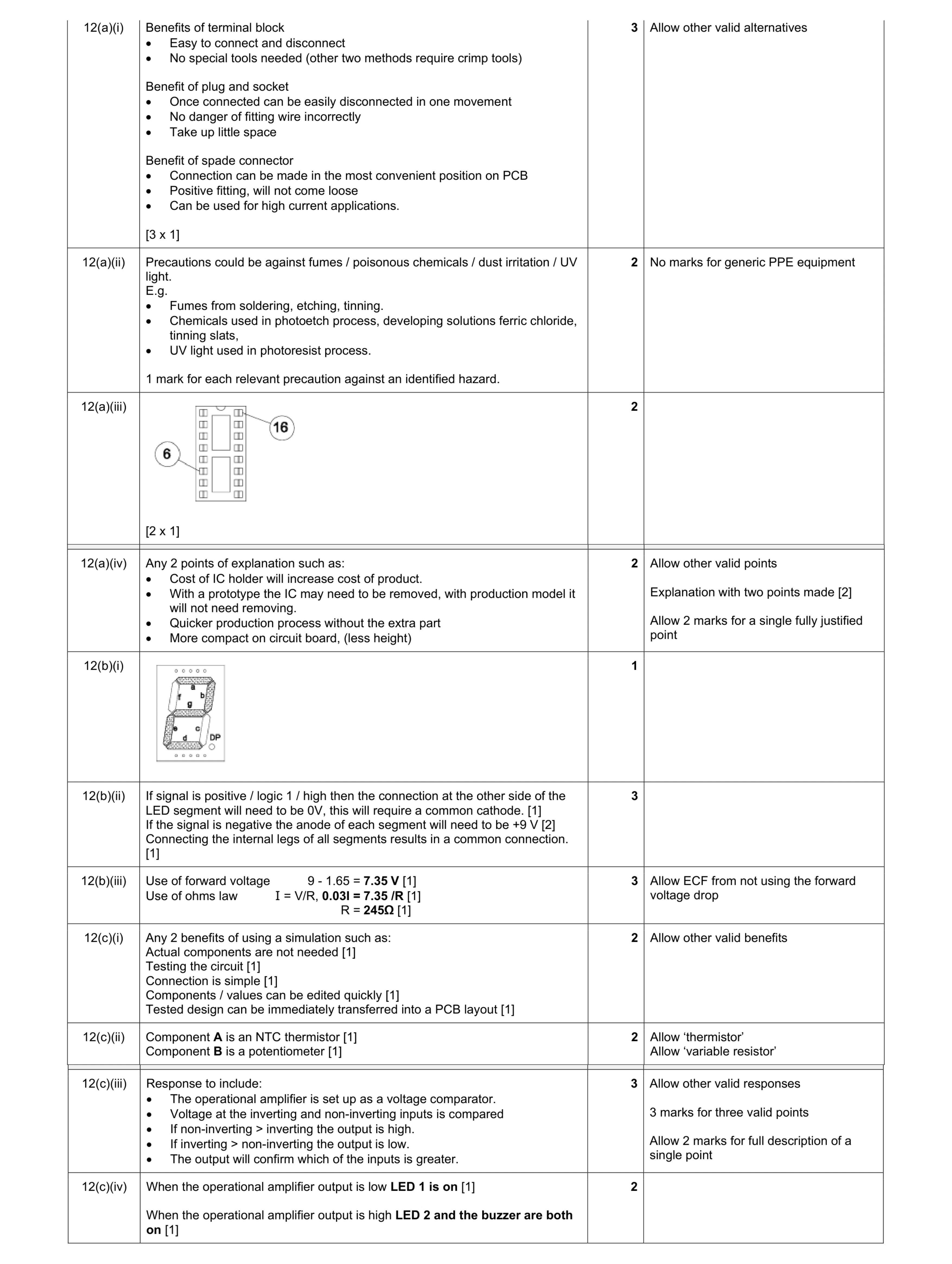 16
16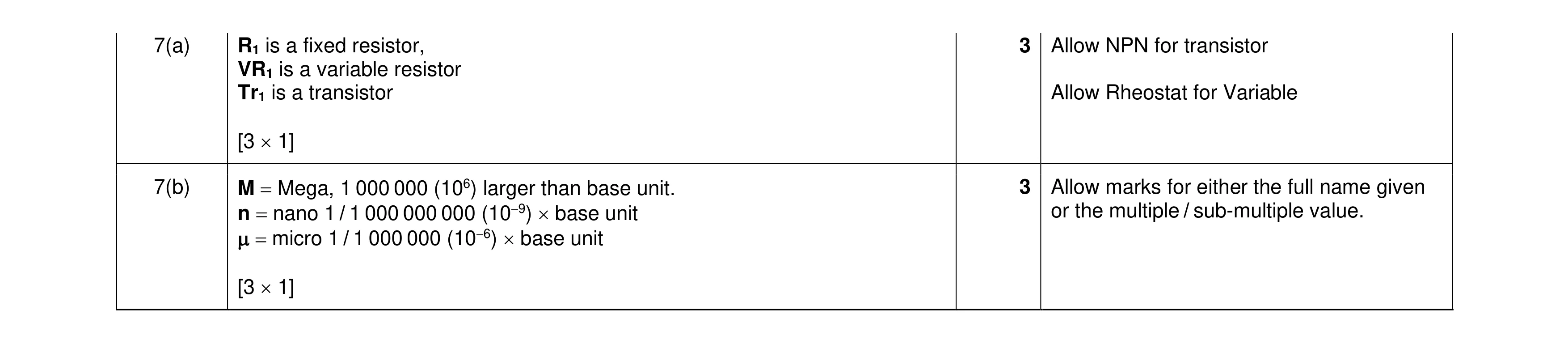 6
6 2
2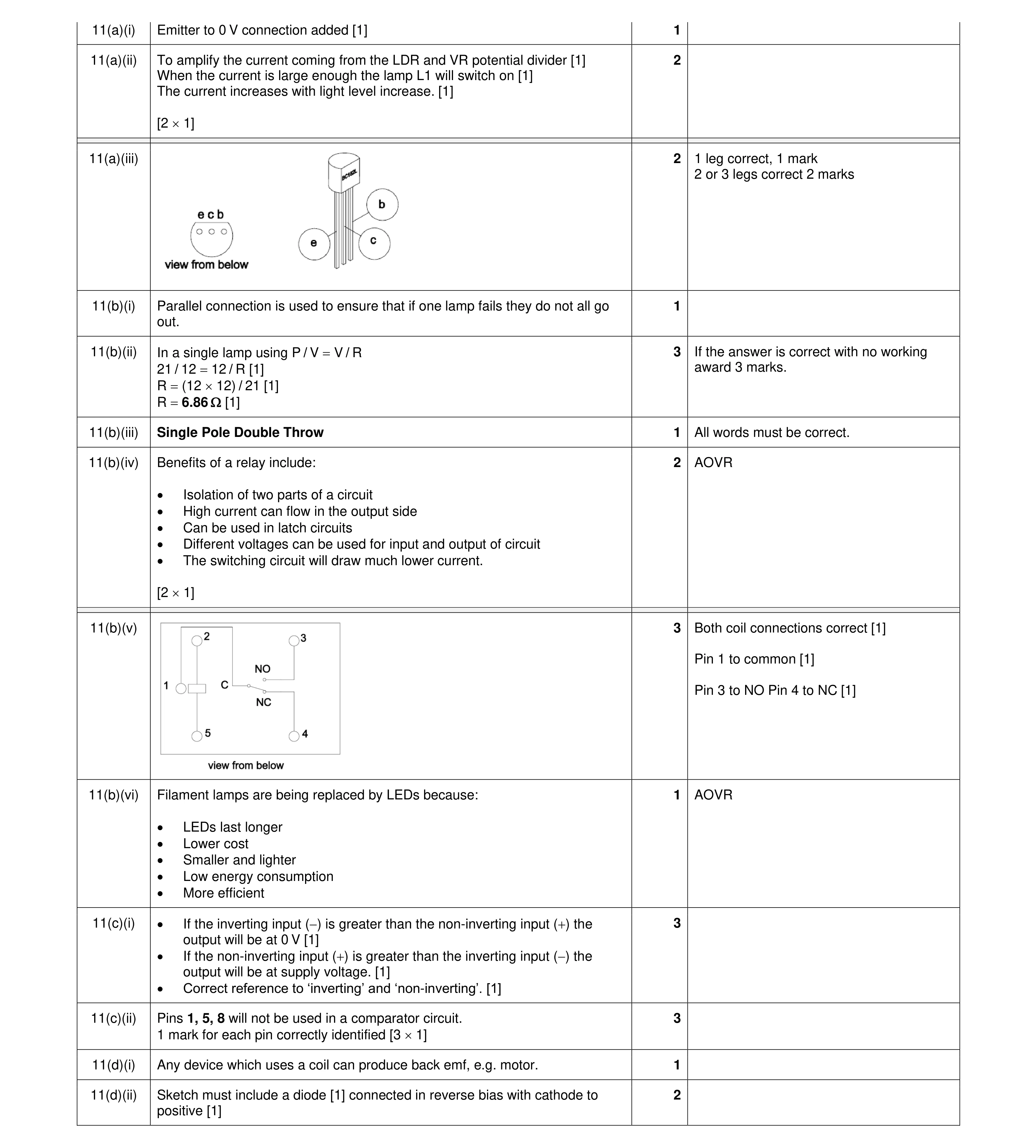 16
16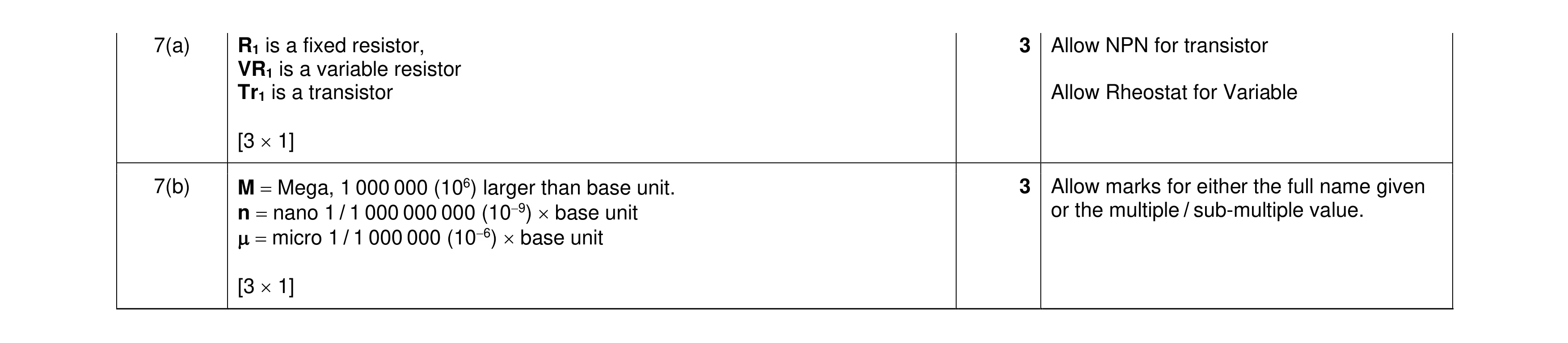 6
6 2
2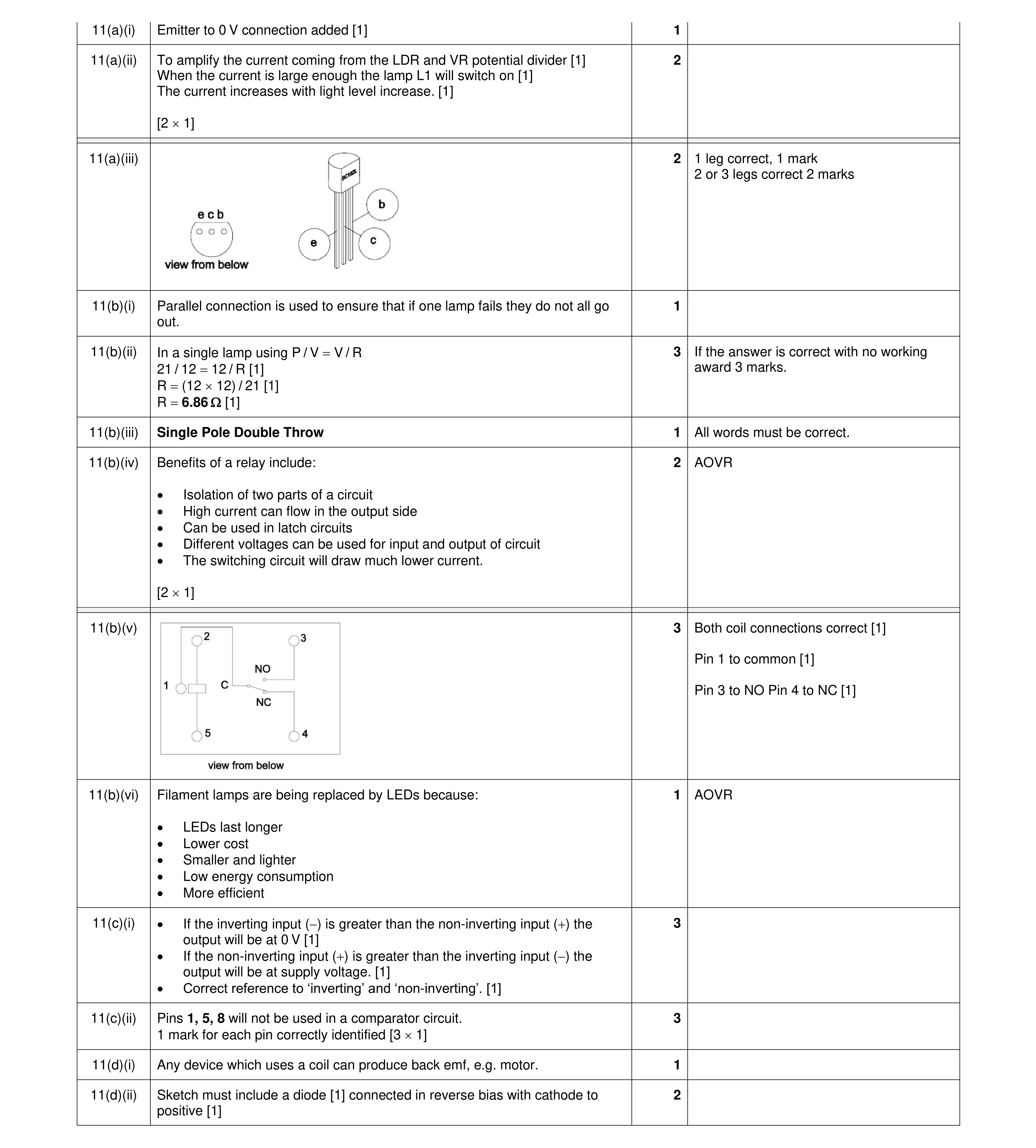 16
16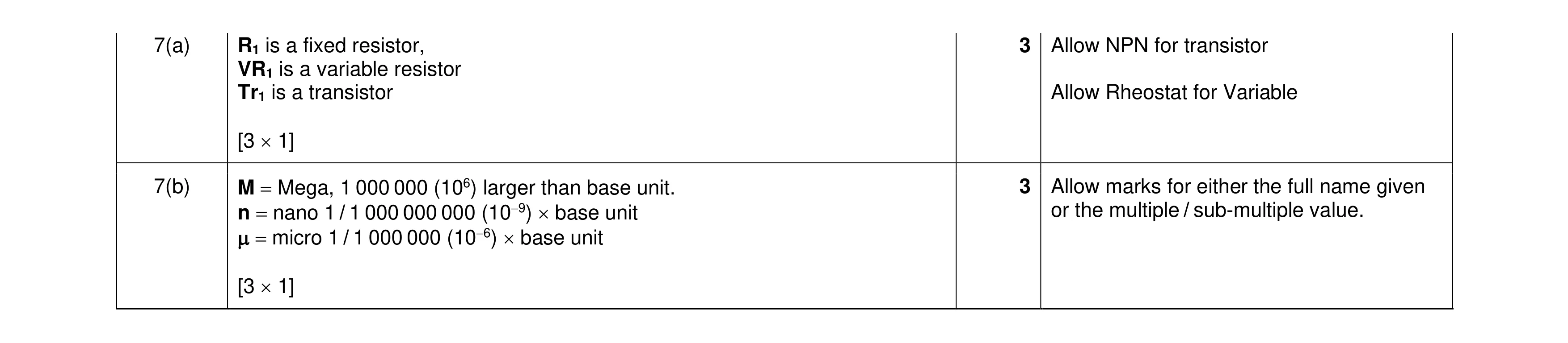 6
6 2
2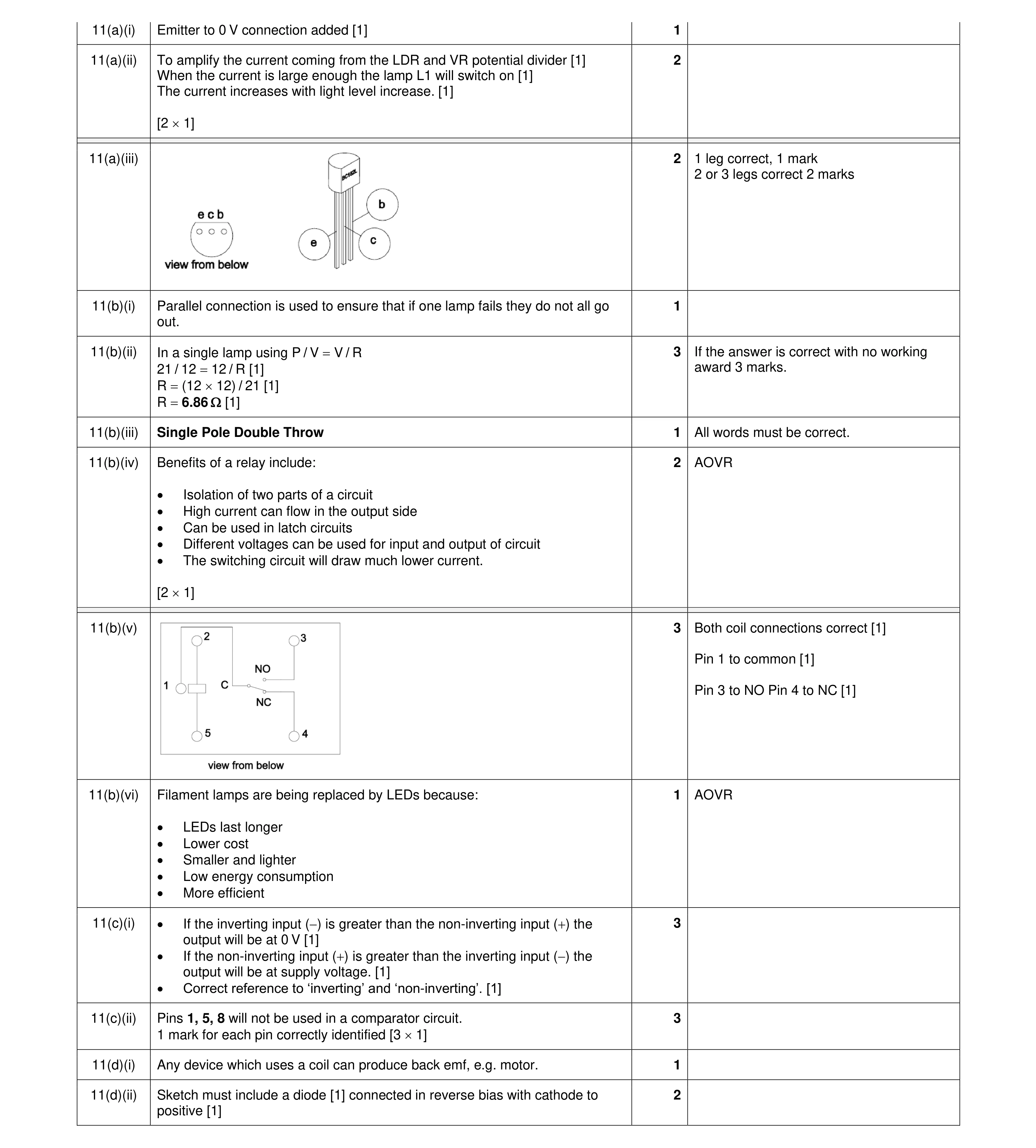 16
16 1
1 3
3 2
2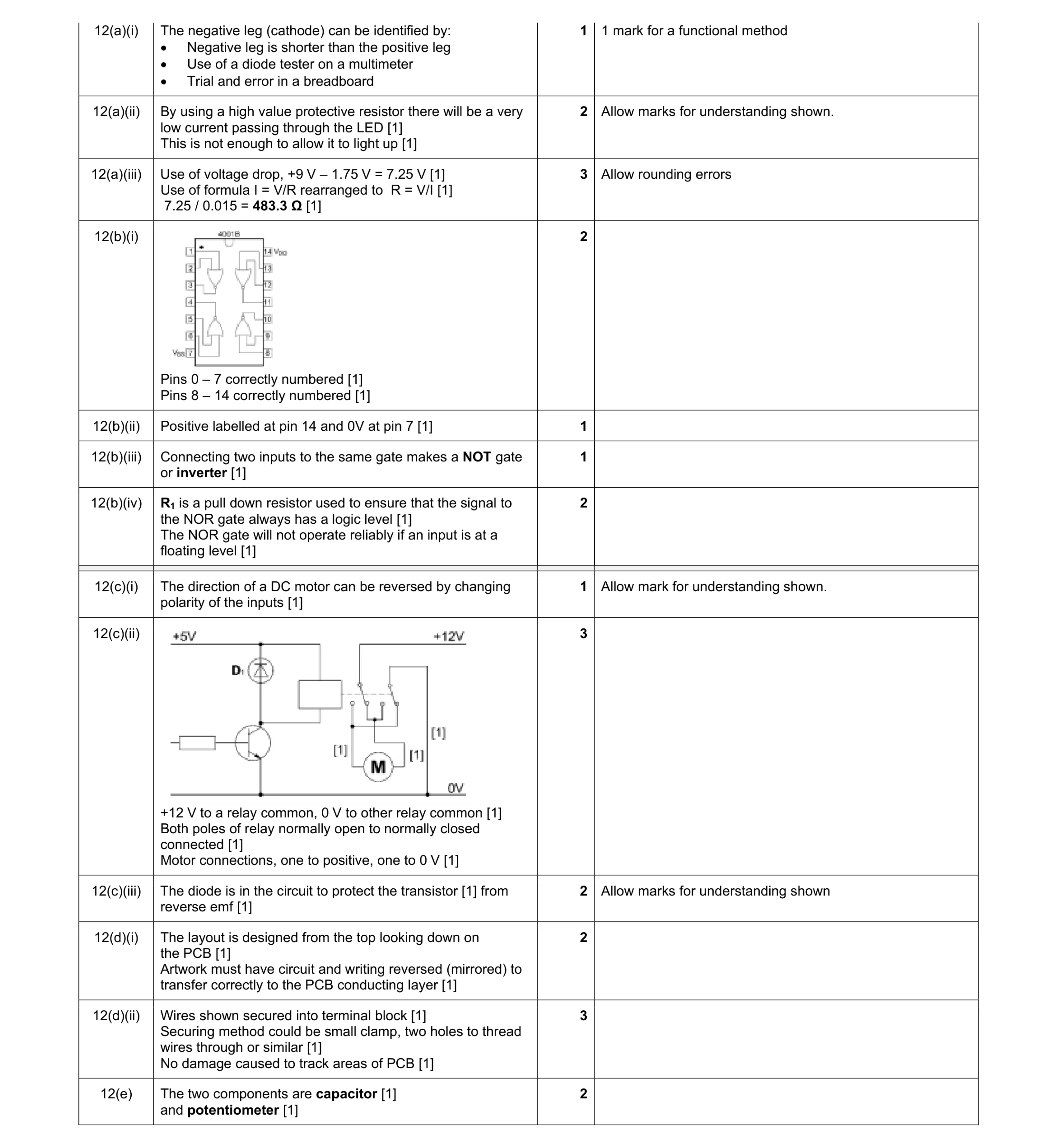 16
16 3
3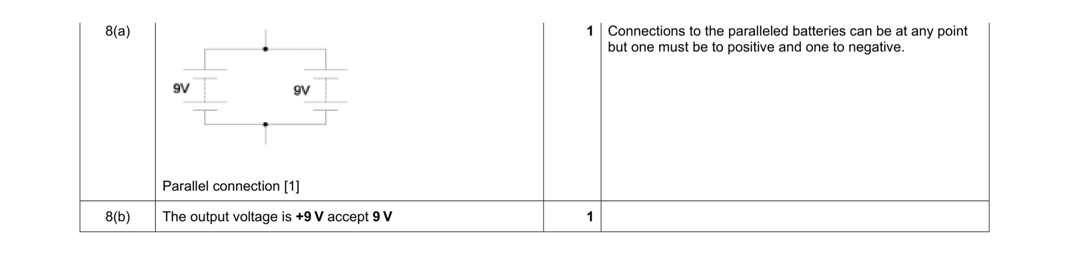 2
2 3
3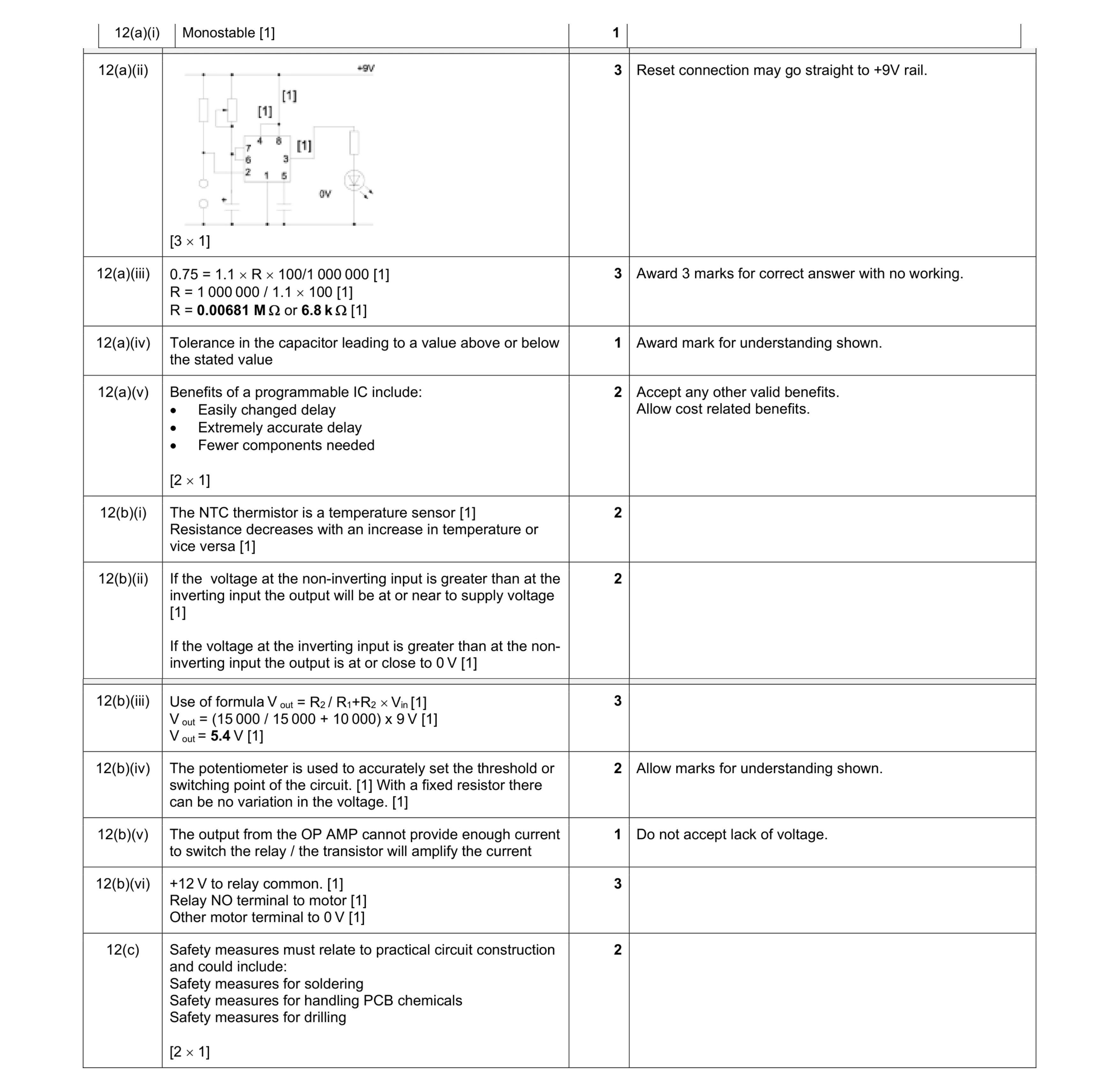 10
10 1
1 3
3 2
2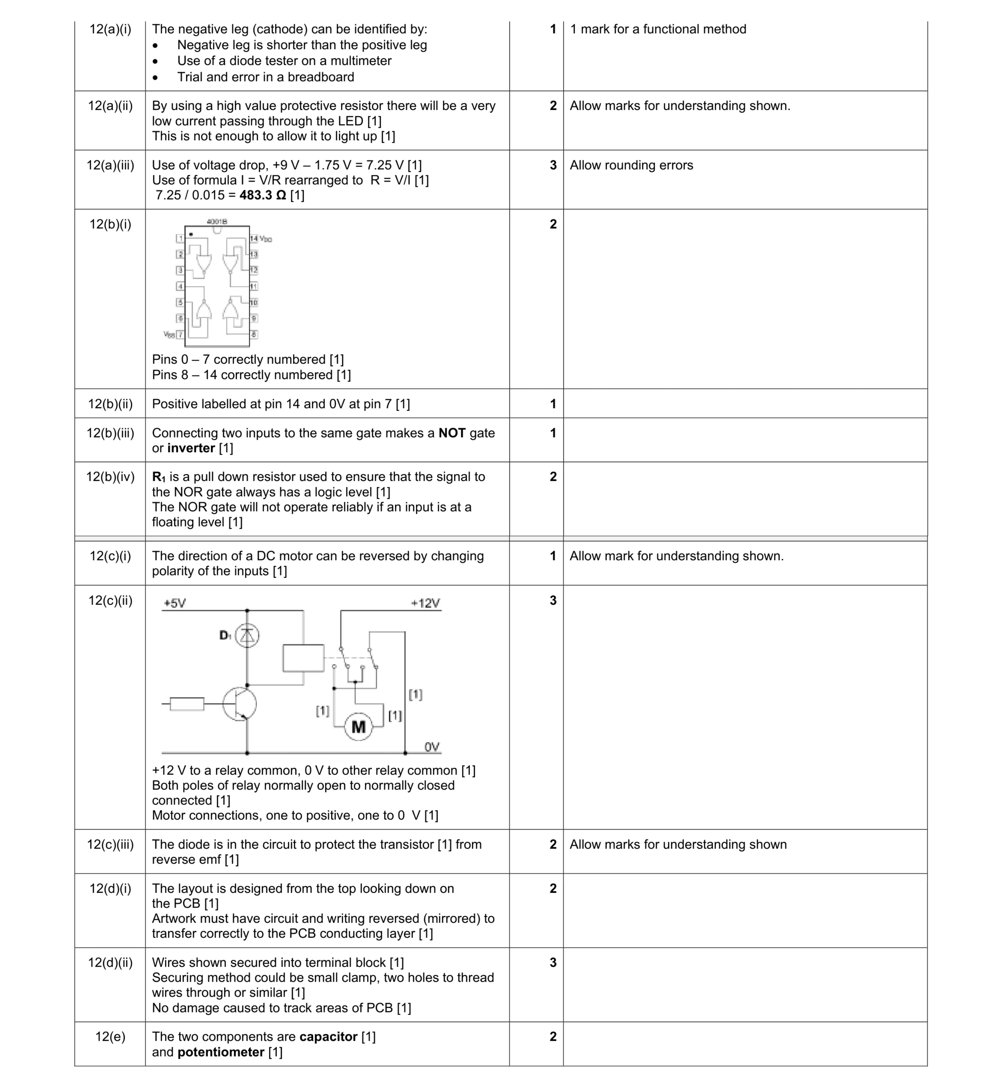 16
16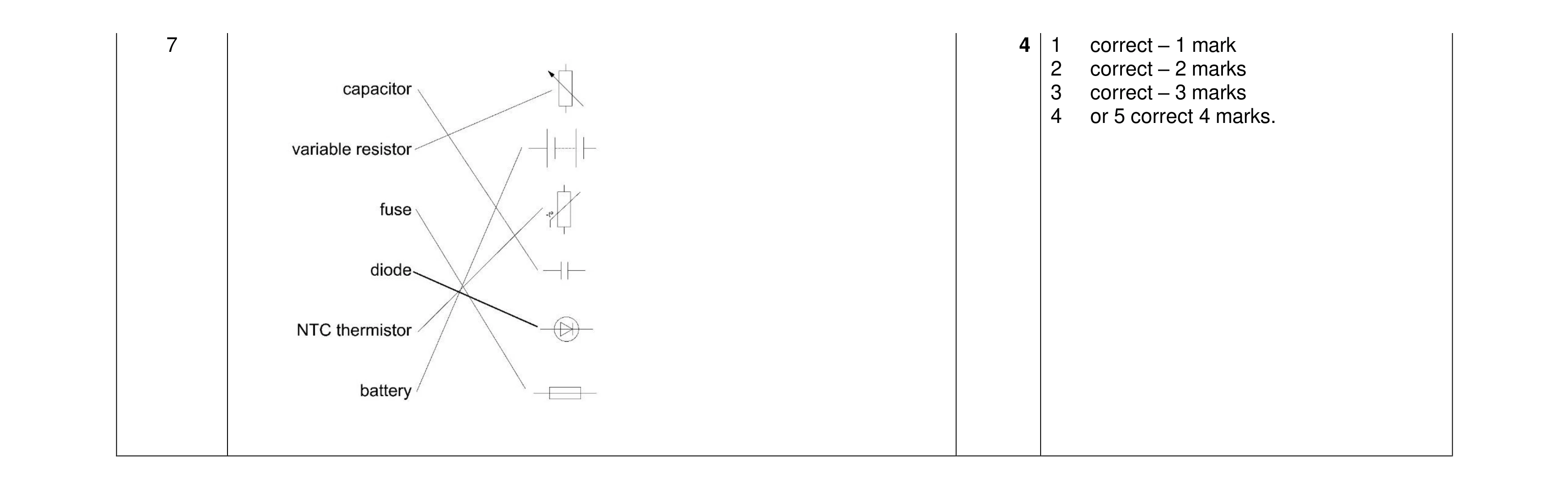 4
4 3
3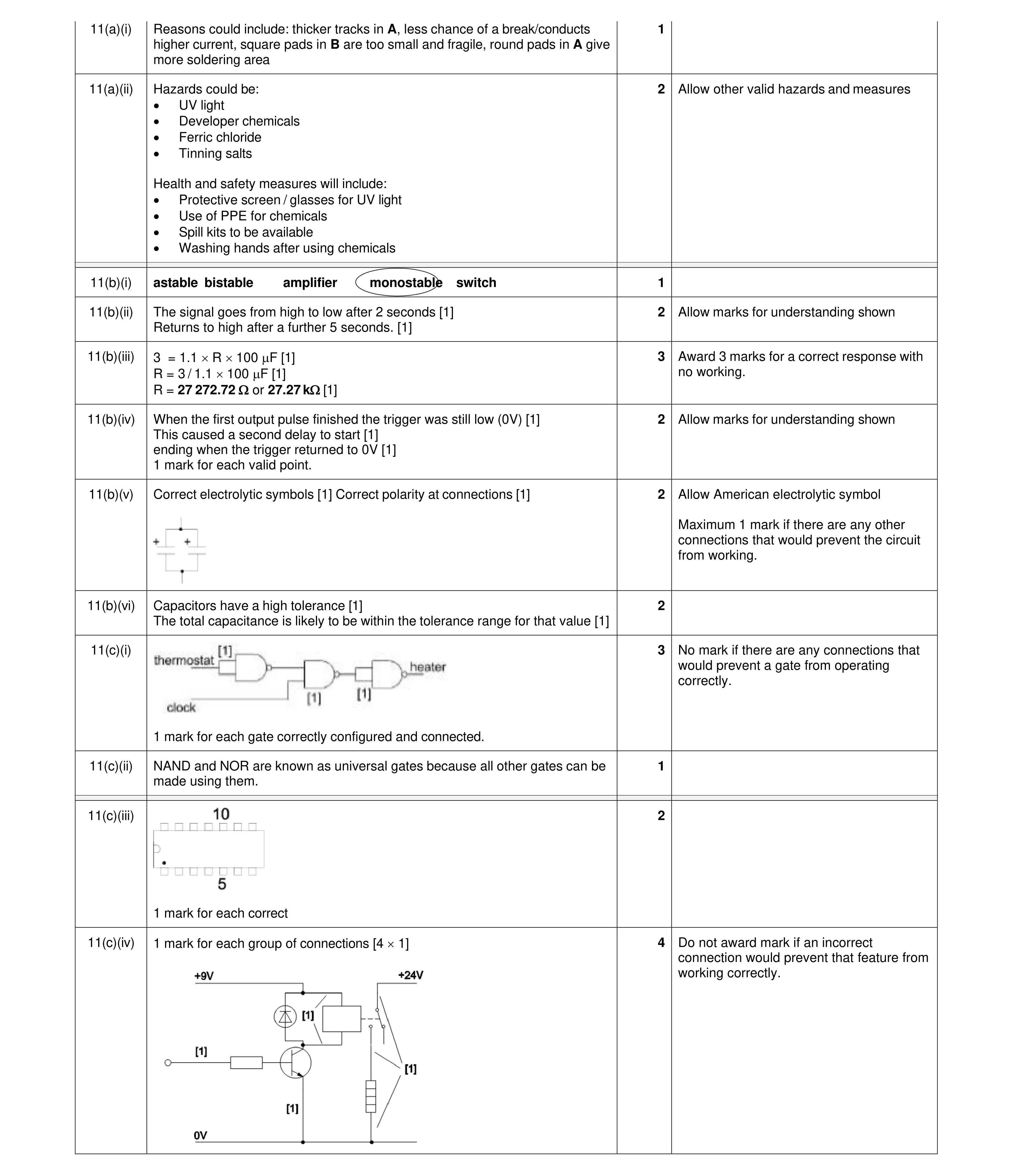 18
18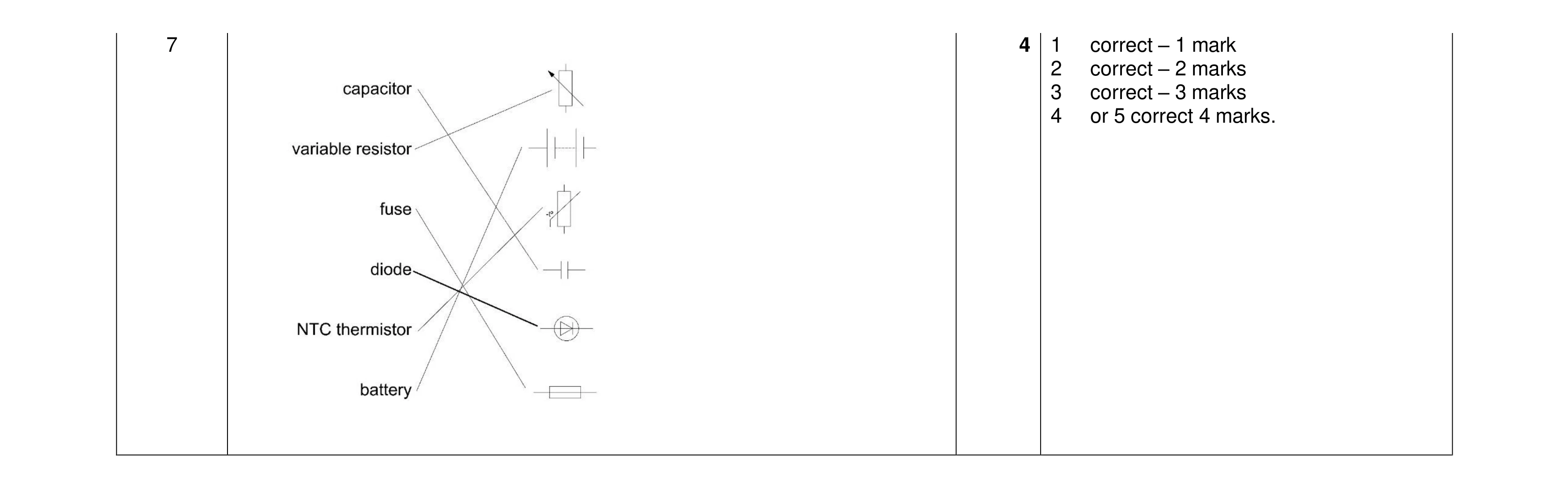 4
4 3
3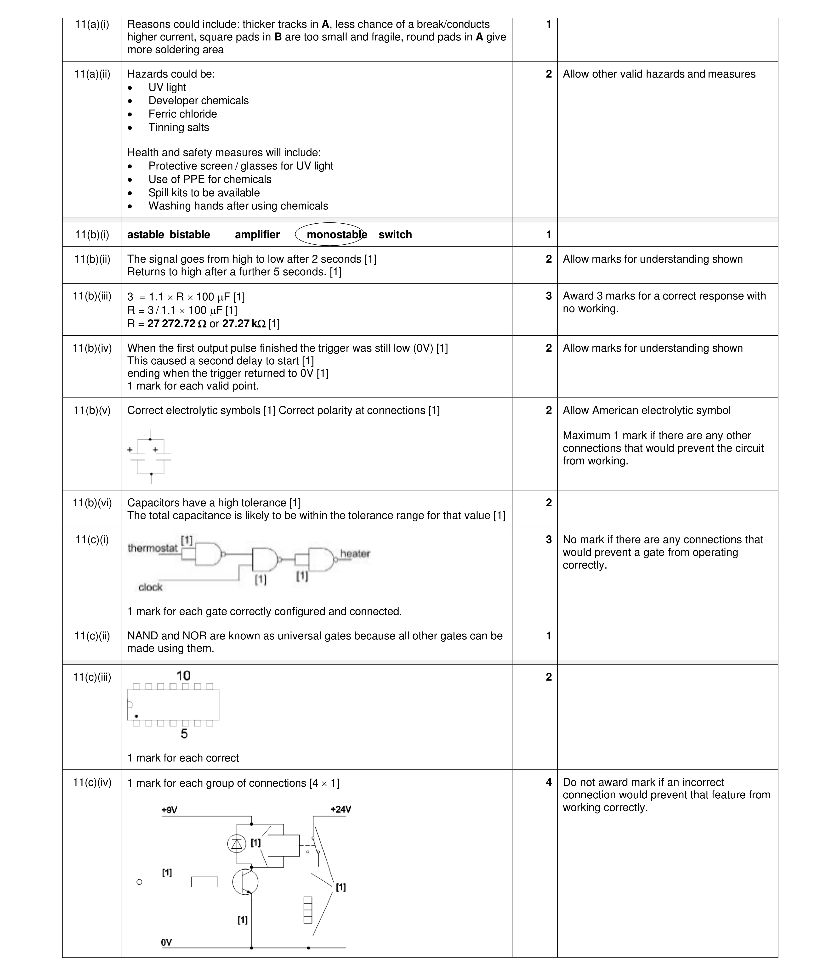 18
18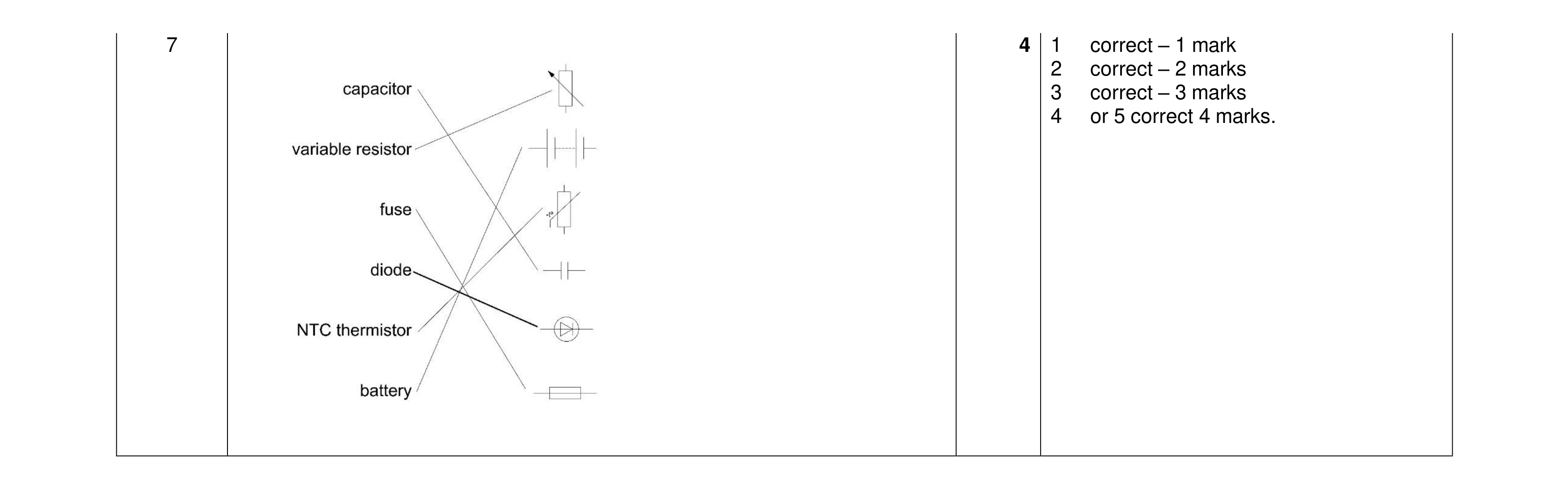 4
4 3
3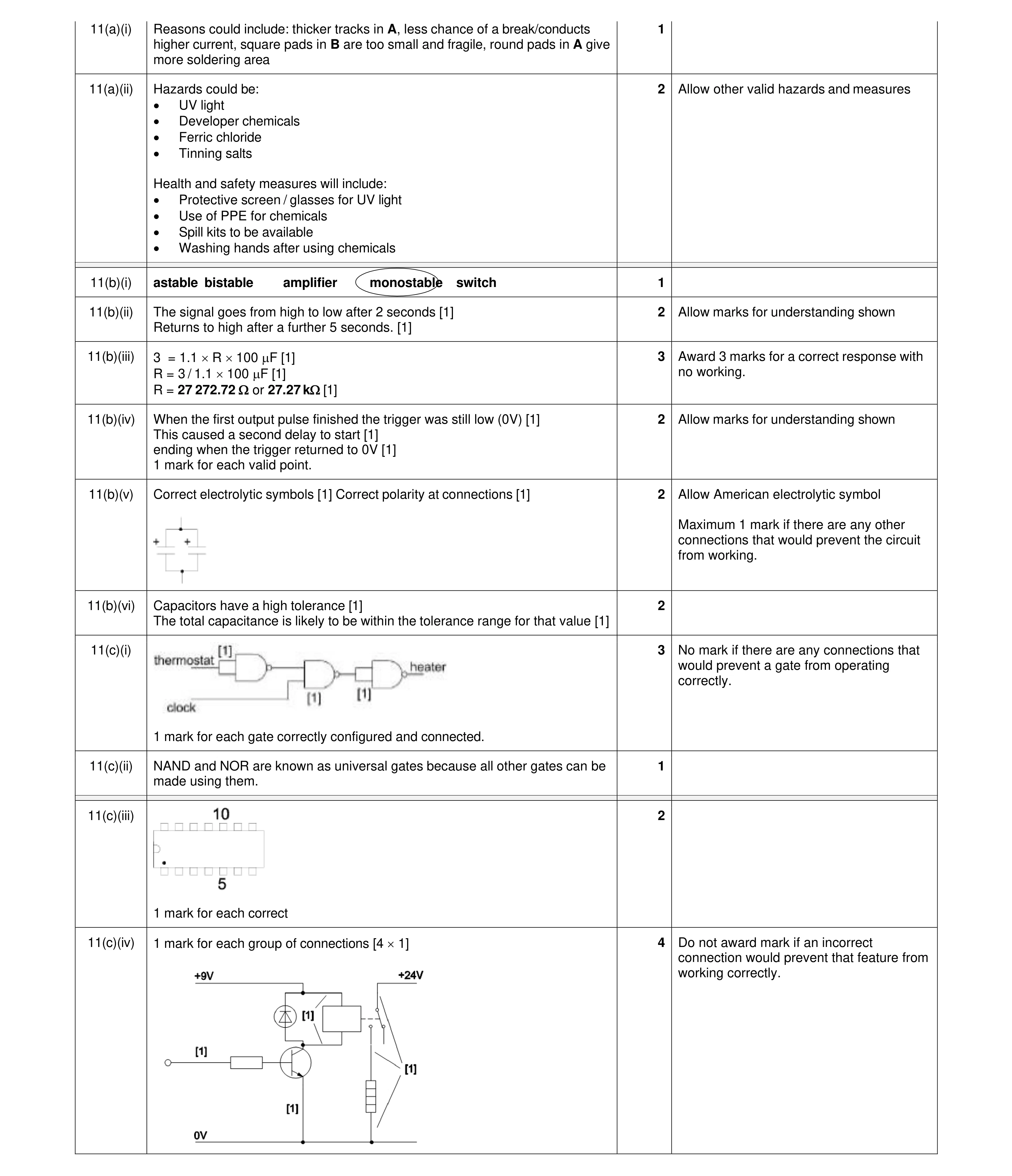 18
18 4
4 4
4 3
3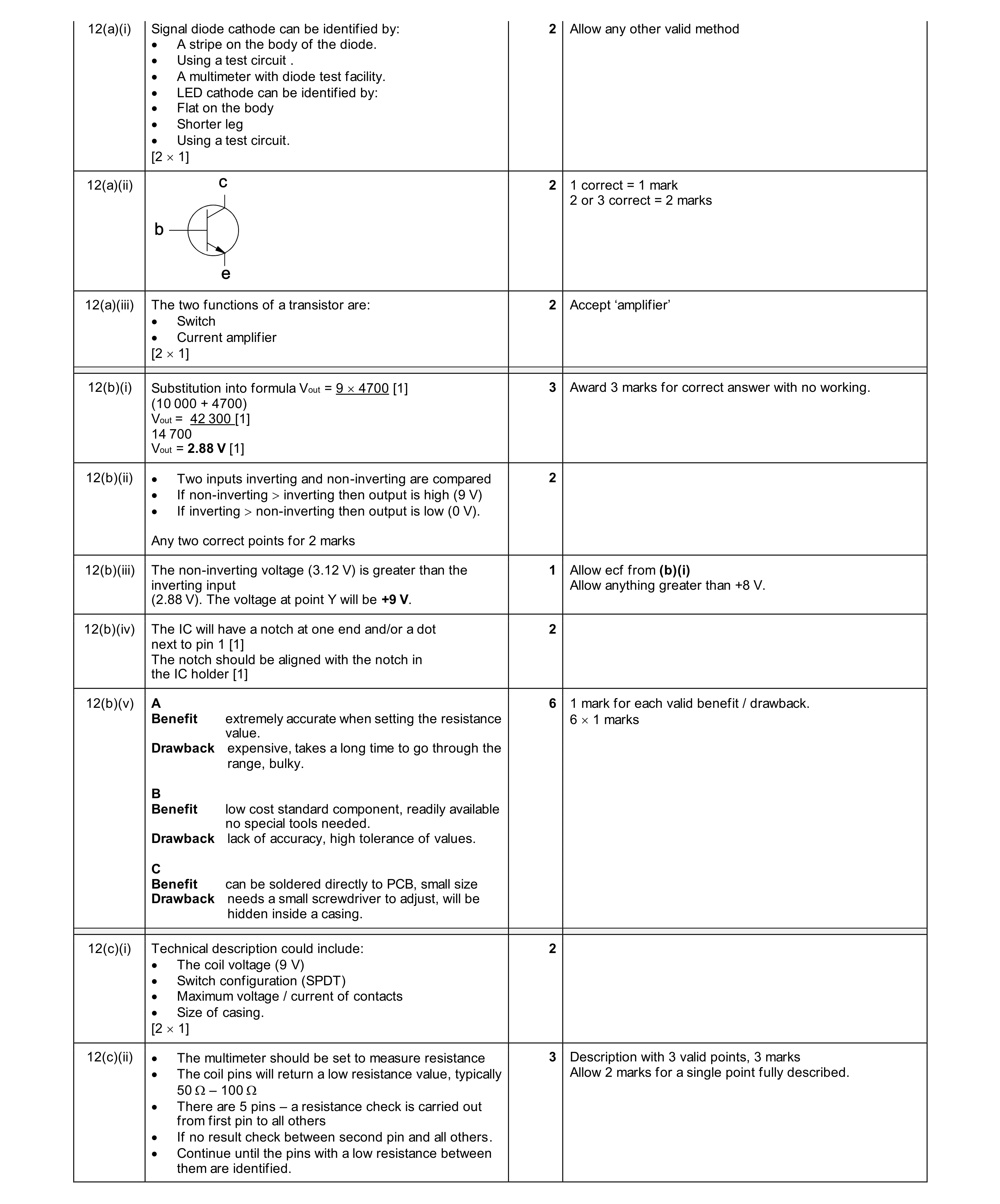 20
20 4
4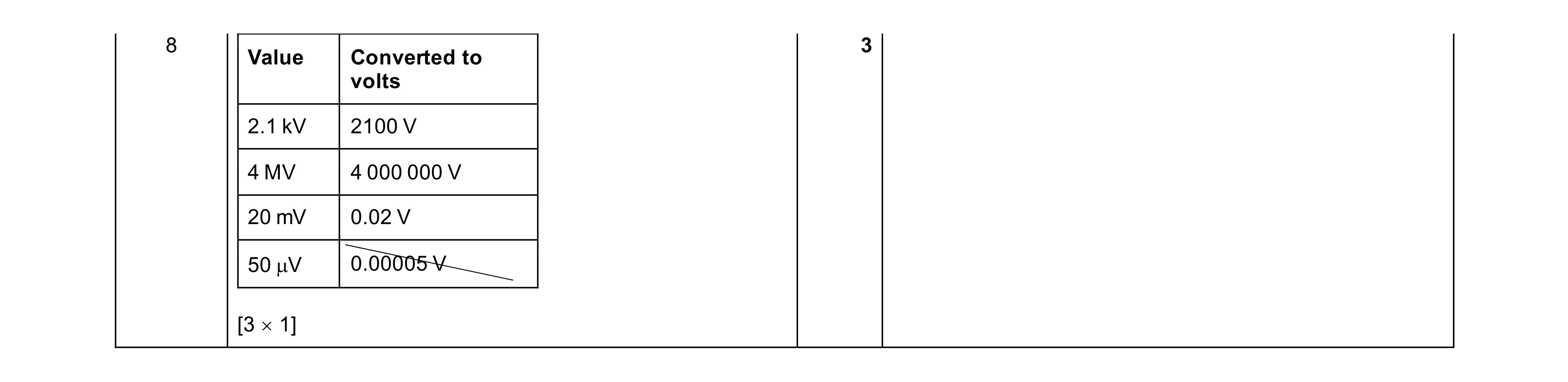 3
3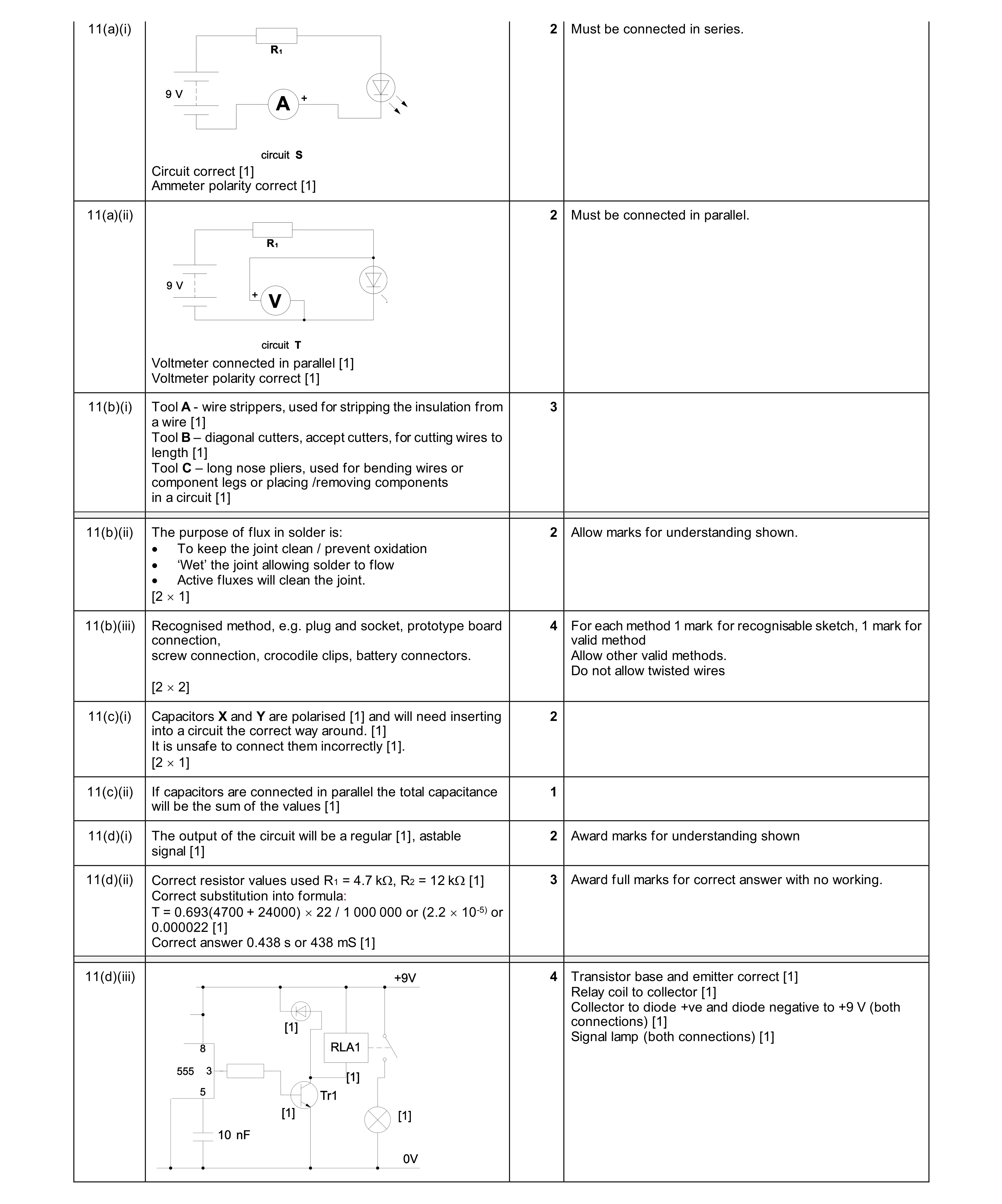 16
16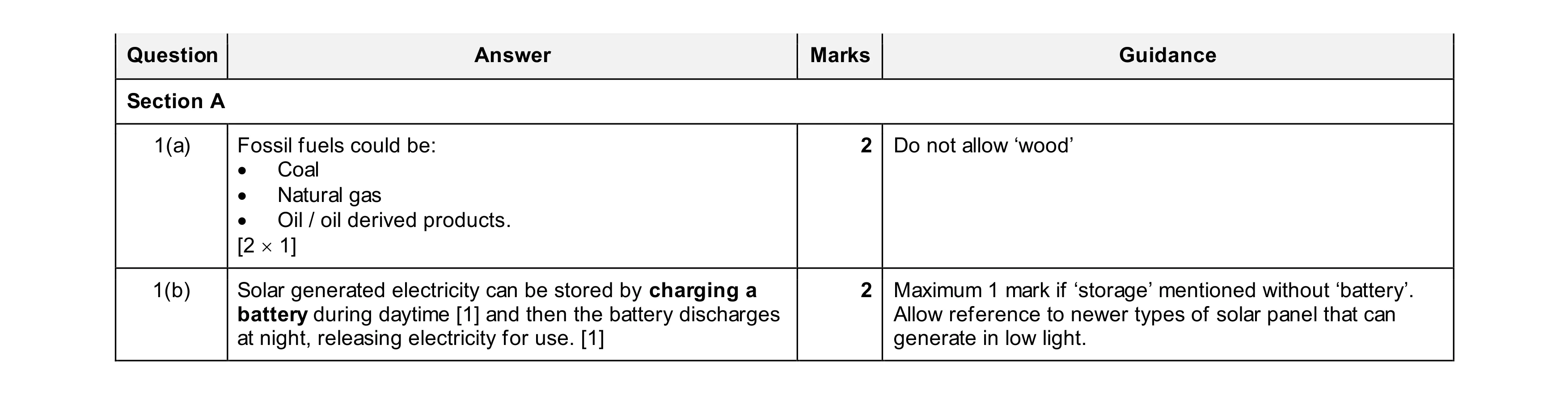 4
4 4
4 3
3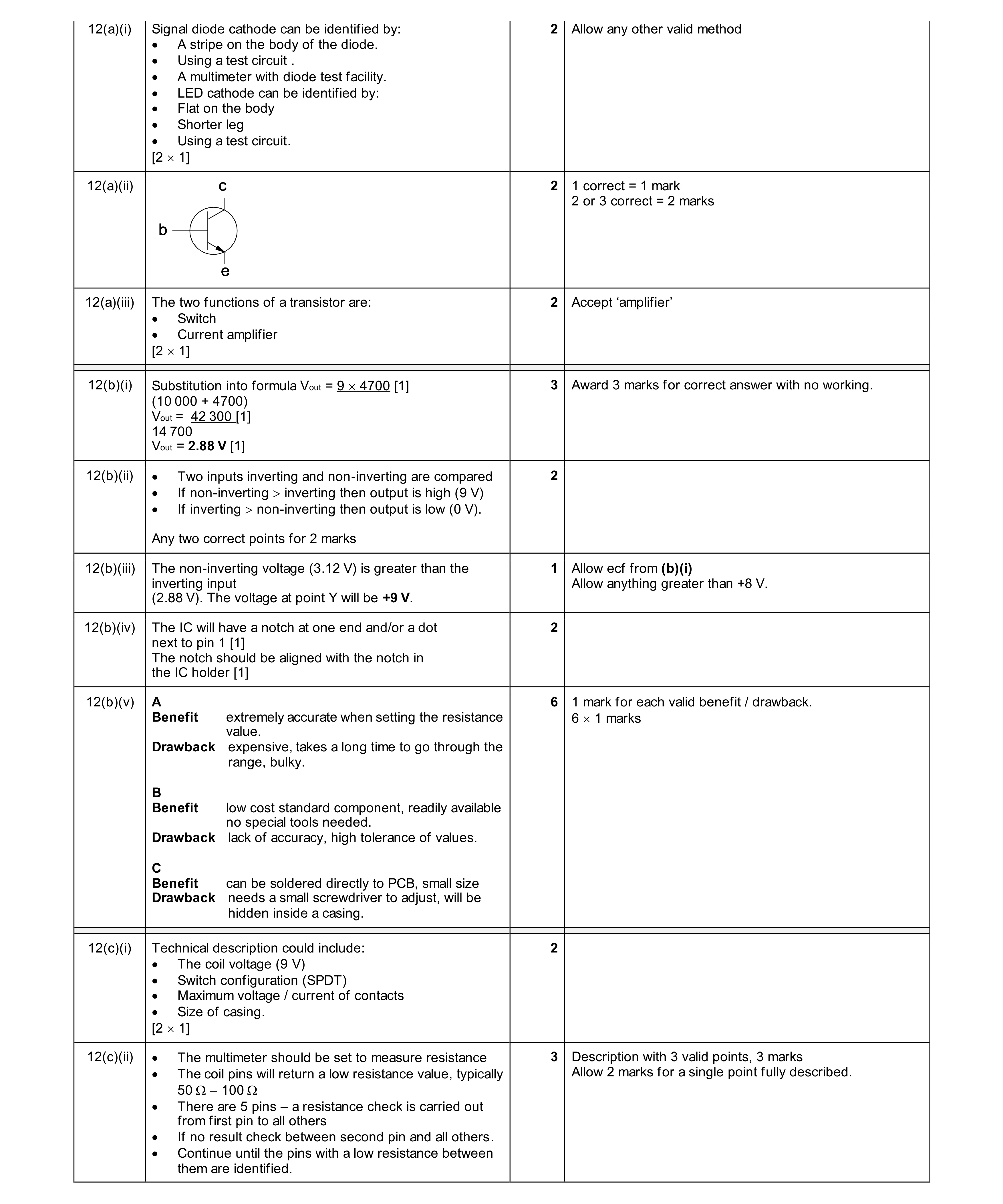 20
20 4
4 1
1 2
2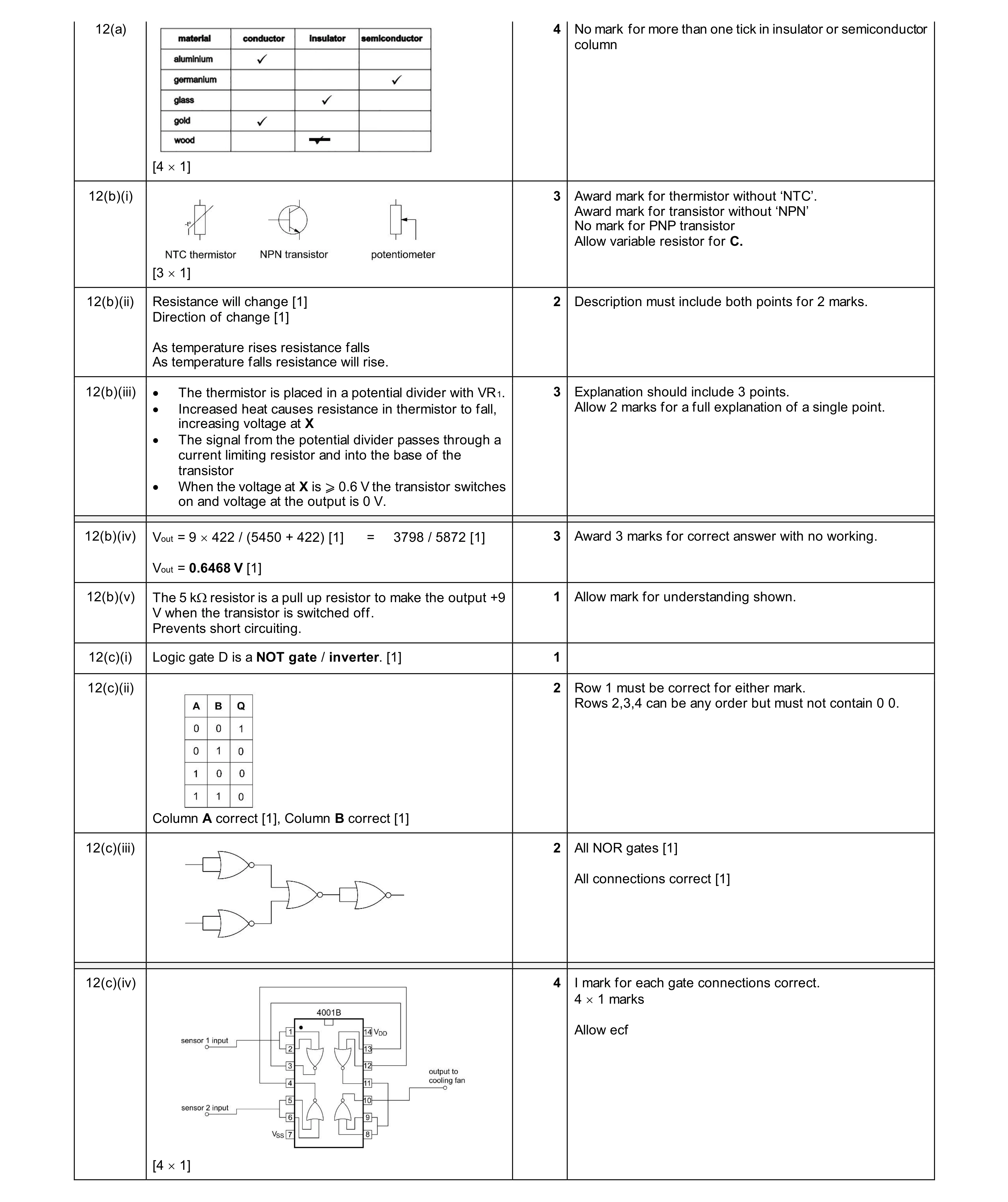 21
21 4
4 1
1 2
2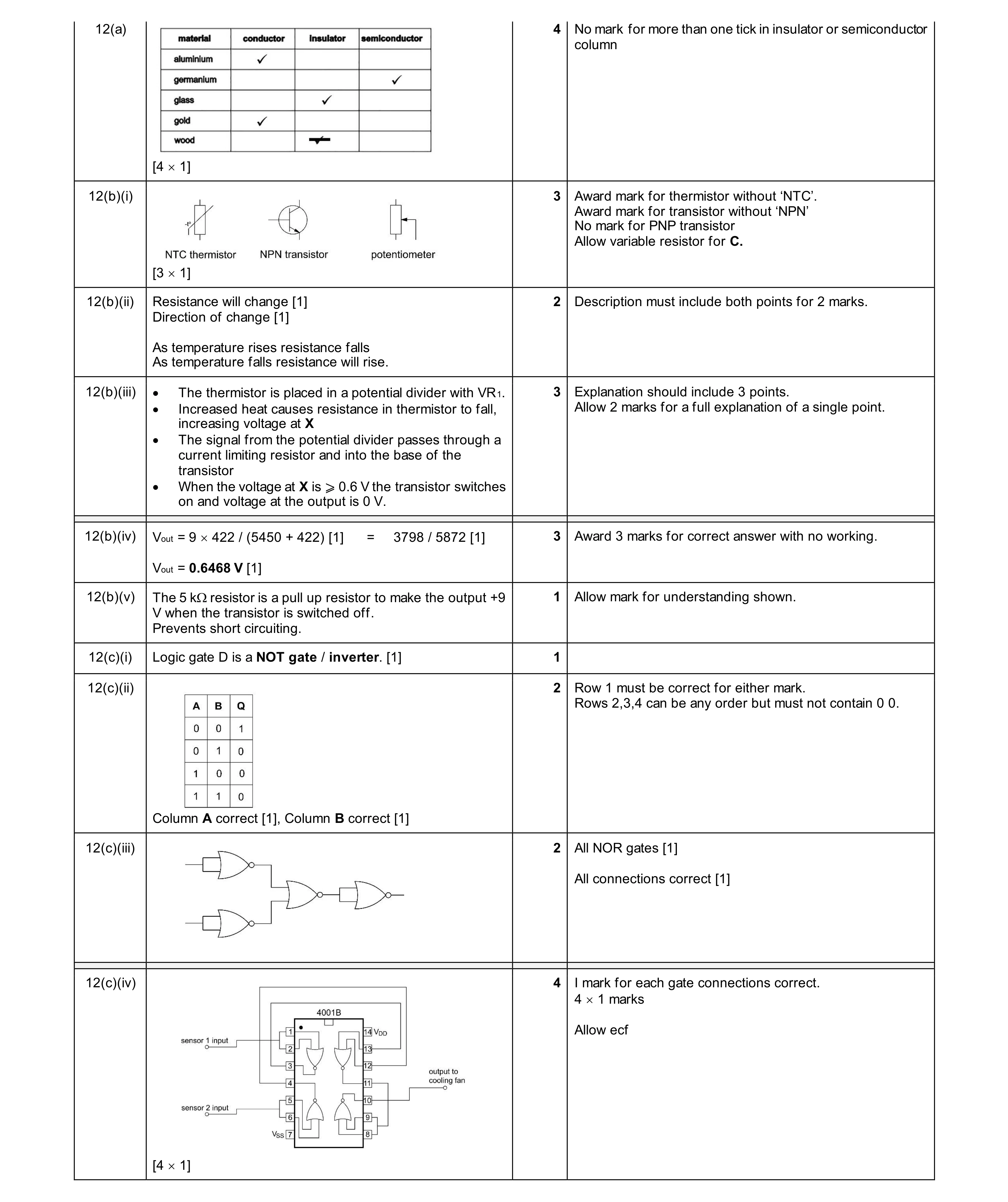 21
21 4
4 1
1 2
2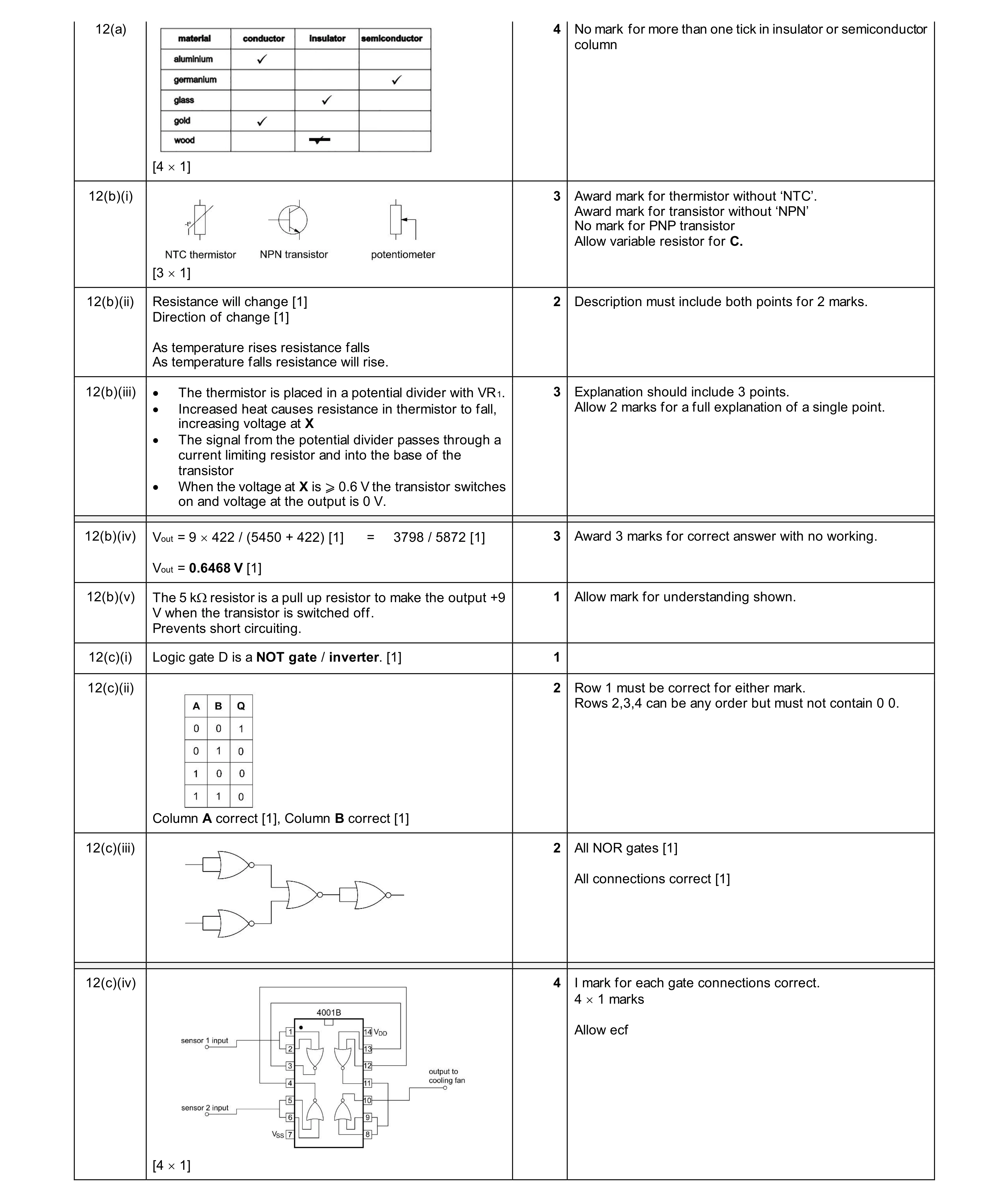 21
21