Questions as text
Q1 · A student designs a circuit incorporating an operational amplifier (op-amp) as shown in… 9702/42 May/June 2017
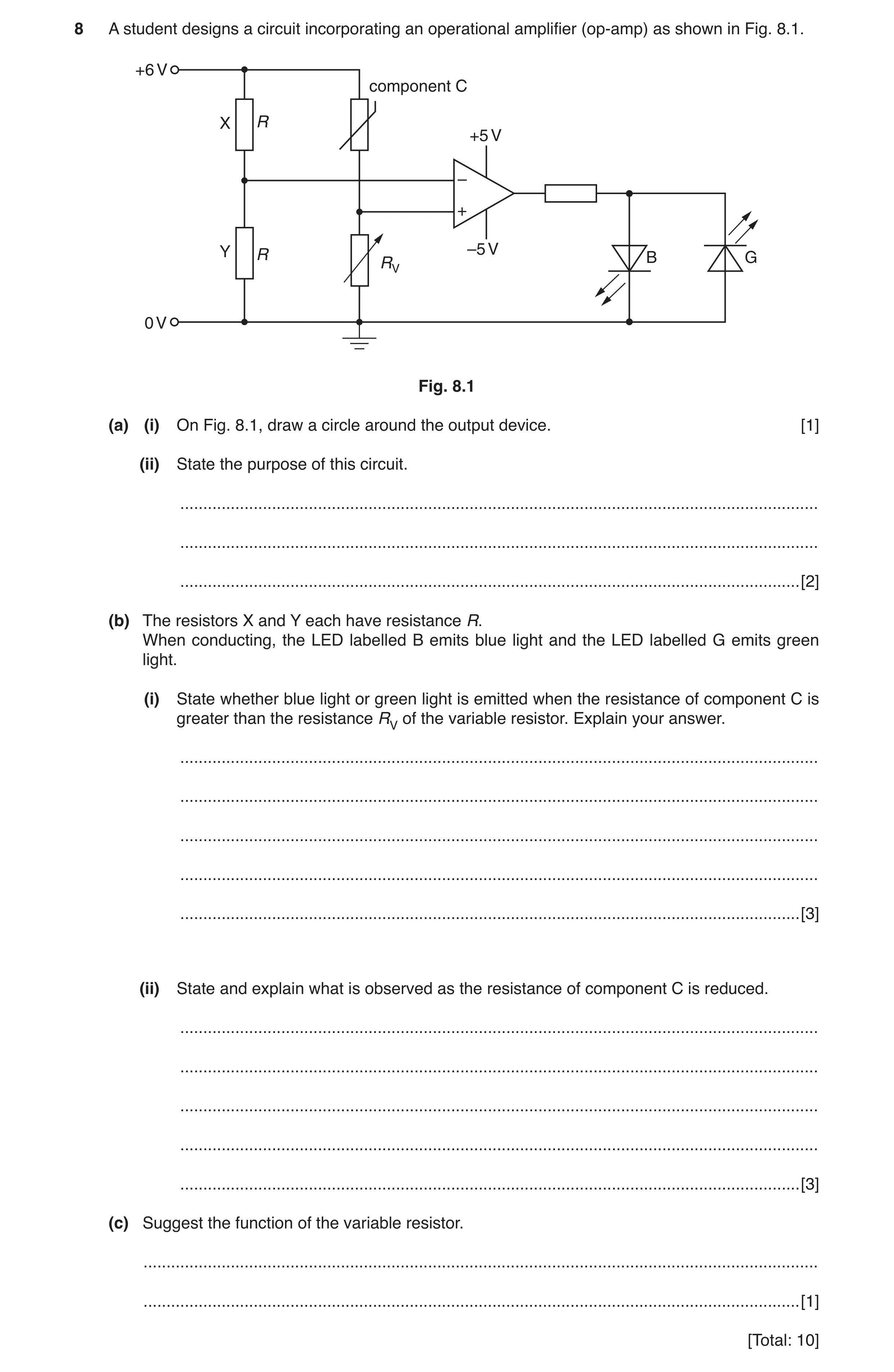
8 A student designs a circuit incorporating an operational amplifier (op-amp) as shown in Fig. 8.1. +6 V component C X R +5 V – + Y R –5 V B G RV 0 V Fig. 8.1 (a) (i) On Fig. 8.1, draw a circle around the output device. [1] (ii) State the purpose of this circuit. … … … [2] (b) The resistors X and Y each have resistance R. When conducting, the LED labelled B emits blue light and the LED labelled G emits green light. (i) State whether blue light or green light is emitted when the resistance of component C is greater than the resistance RV of the variable resistor. Explain your answer. … … … … … [3] (ii) State and explain what is observed as the resistance of component C is reduced. … … … … … [3] (c) Suggest the function of the variable resistor. … … [1] [Total: 10]
10 marks
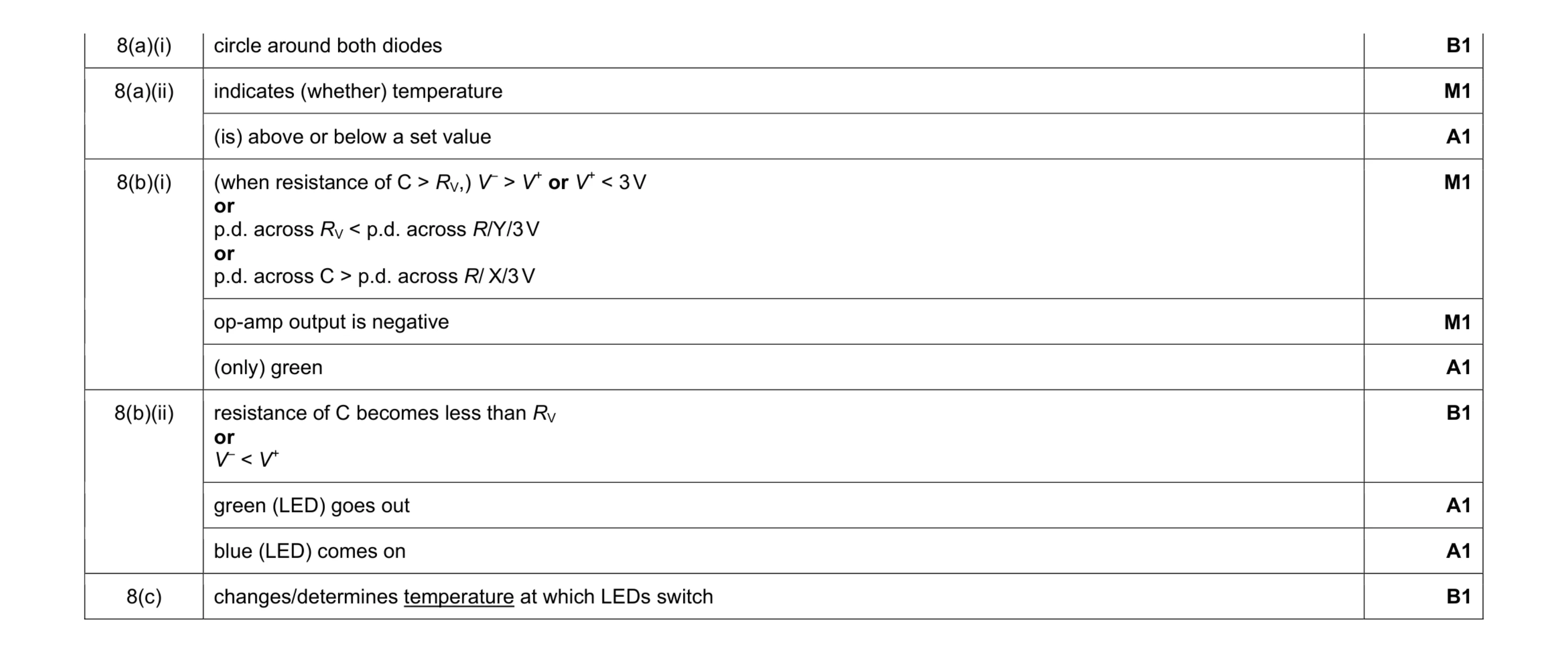
Mark scheme: 8(a)(i) circle around both diodes B1 8(a)(ii) indicates (whether) temperature M1 (is) above or below a set value A1 8(b)(i) (when resistance of C > RV,) V– > V+ or V+ < 3 V or p.d. across RV < p.d. across R/Y/3 V or p.d. across C > p.d. across R/ X/3 V M1 op-amp output is negative M1 (only) green A1 8(b)(ii) resistance of C becomes less than RV or V– < V+ B1 green (LED) goes out A1 blue (LED) comes on A1 8(c) changes/determines temperature at which LEDs switch B1
This question in 9702/42 May/June 2017
Q2 · Feedback is used frequently in amplifier circuits 9702/42 Oct/Nov 2017
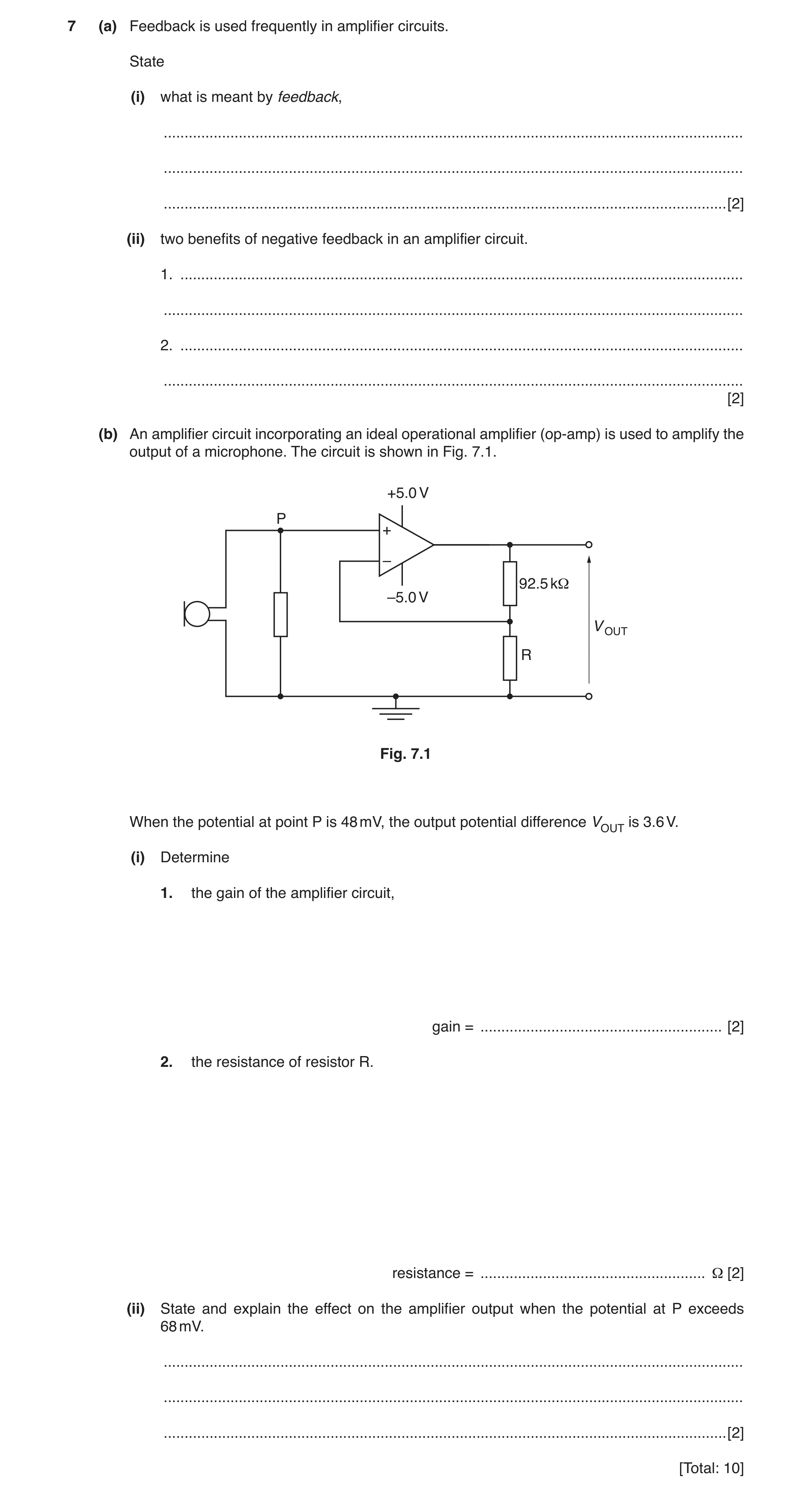
7 (a) Feedback is used frequently in amplifier circuits. State (i) what is meant by feedback, … … … [2] (ii) two benefits of negative feedback in an amplifier circuit. 1. … … 2. … … [2] (b) An amplifier circuit incorporating an ideal operational amplifier (op-amp) is used to amplify the output of a microphone. The circuit is shown in Fig. 7.1. +5.0 V P + – 92.5 kΩ –5.0 V V OUT R Fig. 7.1 When the potential at point P is 48 mV, the output potential difference VOUT is 3.6 V. (i) Determine 1. the gain of the amplifier circuit, gain = … [2] 2. the resistance of resistor R. resistance = … Ω [2] (ii) State and explain the effect on the amplifier output when the potential at P exceeds 68 mV. … … … [2] [Total: 10]
10 marks
Mark scheme: 7(a)(i) (part of) the output is combined with the input M1 reference to potential/voltage/signal A1 7(a)(ii) • increased (operating) stability • increased bandwidth/range of frequencies over which gain is constant • less distortion (of output) Any 2 points. B2 7(b)(i) 1. gain = 3.6 / (48 × 10–3) C1 = 75 A1 2. gain = 1 + RF / R 75 = 1 + (92.5 × 10³) / R C1 R = 1300 Ω A1 7(b)(ii) for 68 mV, gain × VIN = 5.1 (V) or output voltage would be greater than the supply voltage M1 amplifier would saturate (at 5.0 V) or output voltage = 5.0 (V) A1
This question in 9702/42 Oct/Nov 2017
Q3 · The circuit of an amplifier incorporating an ideal operational amplifier (op-amp) is… 9702/43 Oct/Nov 2017
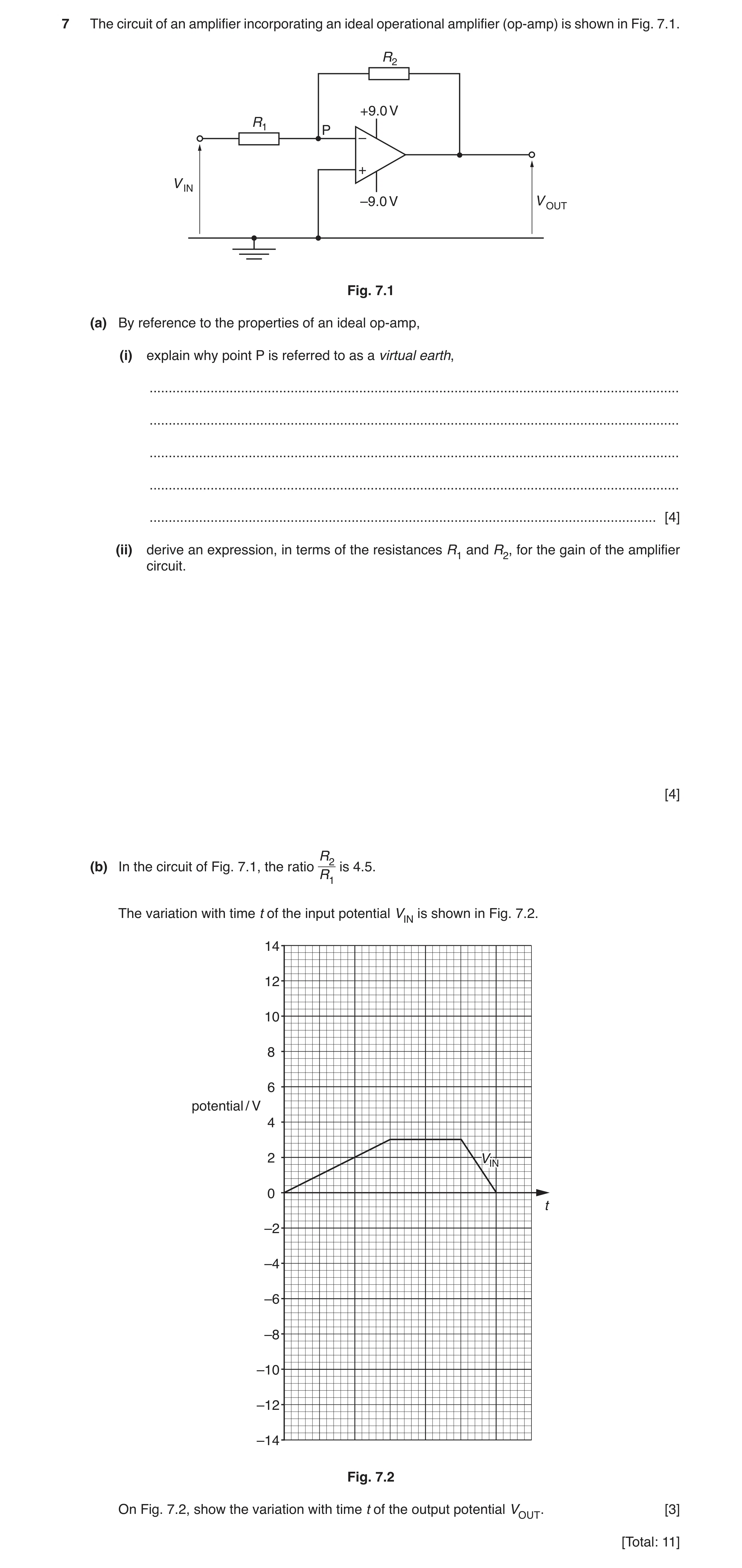
7 The circuit of an amplifier incorporating an ideal operational amplifier (op-amp) is shown in Fig. 7.1. R2 +9.0 V R1 P – + V IN –9.0 V V OUT Fig. 7.1 (a) By reference to the properties of an ideal op-amp, (i) explain why point P is referred to as a virtual earth, … … … … … [4] (ii) derive an expression, in terms of the resistances R1 and R2, for the gain of the amplifier circuit. [4] R2(b) In the circuit of Fig. 7.1, the ratio is 4.5. R1 The variation with time t of the input potential VIN is shown in Fig. 7.2. 14 12 10 8 6 potential / V 4 2 VINVIN 0 t –2 –4 –6 –8 –10 –12 –14 Fig. 7.2 On Fig. 7.2, show the variation with time t of the output potential VOUT. [3] [Total: 11]
11 marks
Mark scheme: 7(a)(i) gain of amplifier is very large B1 V+ is at earth (potential) B1 for amplifier not to saturate M1 difference between V– and V+ must be very small or V– must be equal to V+ A1 or if V– ≠ V+ then feedback voltage (M1) acts to reduce gap until V– = V+ when stable (A1) 7(a)(ii) input impedance is infinite B1 (so) current in R1 = current in R2 B1 (VIN – 0) / R1 = (0 – VOUT) / R2 B1 (gain =) VOUT / VIN = – R2 / R1 B1 7(b) graph: correct inverted shape (straight diagonal line from (0,0) to a negative potential, then a horizontal line, then a straight diagonal line back to the t-axis at the point where VIN = 0) B1 horizontal line at correct potential of (–)9.0 V B1 both ends of horizontal line occur at correct times (coinciding with when VIN = 2.0 V) B1
This question in 9702/43 Oct/Nov 2017
Q4 · Two properties of an ideal operational amplifier (op-amp) are infinite bandwidth and… 9702/42 Feb/March 2018
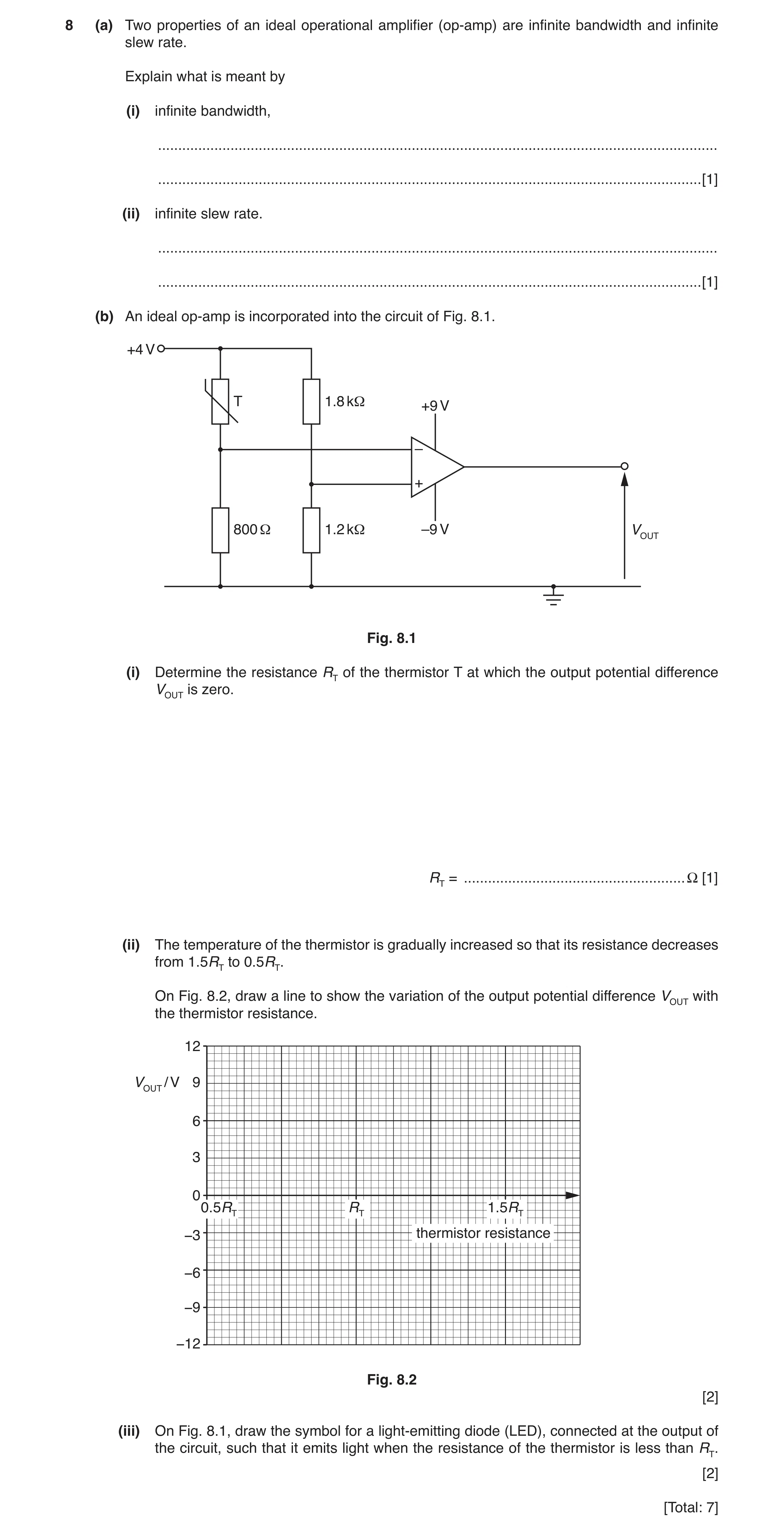
8 (a) Two properties of an ideal operational amplifier (op-amp) are infinite bandwidth and infinite slew rate. Explain what is meant by (i) infinite bandwidth, … … [1] (ii) infinite slew rate. … … [1] (b) An ideal op-amp is incorporated into the circuit of Fig. 8.1. +4 V T 1.8 kΩ +9 V – + 800 Ω 1.2 kΩ –9 V VOUT Fig. 8.1 (i) Determine the resistance RT of the thermistor T at which the output potential difference VOUT is zero. RT = … Ω [1] (ii) The temperature of the thermistor is gradually increased so that its resistance decreases from 1.5RT to 0.5RT. On Fig. 8.2, draw a line to show the variation of the output potential difference VOUT with the thermistor resistance. 12 VOUT / V 9 6 3 0 0.5RT RT 1.5RT −3 thermistor resistance −6 −9 −12 Fig. 8.2 [2] (iii) On Fig. 8.1, draw the symbol for a light-emitting diode (LED), connected at the output of the circuit, such that it emits light when the resistance of the thermistor is less than RT. [2] [Total: 7]
7 marks
Mark scheme: 8(a)(i) all frequencies have the same gain B1 8(a)(ii) output changes at the same time as input changes B1 8(b)(i) RT / 800 = 1.8 / 1.2 RT = 1200 Ω A1 8(b)(ii) stepped from –9 V to +9 V or v.v. B1 Vout negative < RT and Vout positive > RT B1 8(b)(iii) correct LED symbol with connection between VOUT and earth B1 diode pointing upwards B1
This question in 9702/42 Feb/March 2018
Q5 · Negative feedback is often used in amplifiers incorporating an operational amplifier… 9702/41 May/June 2018
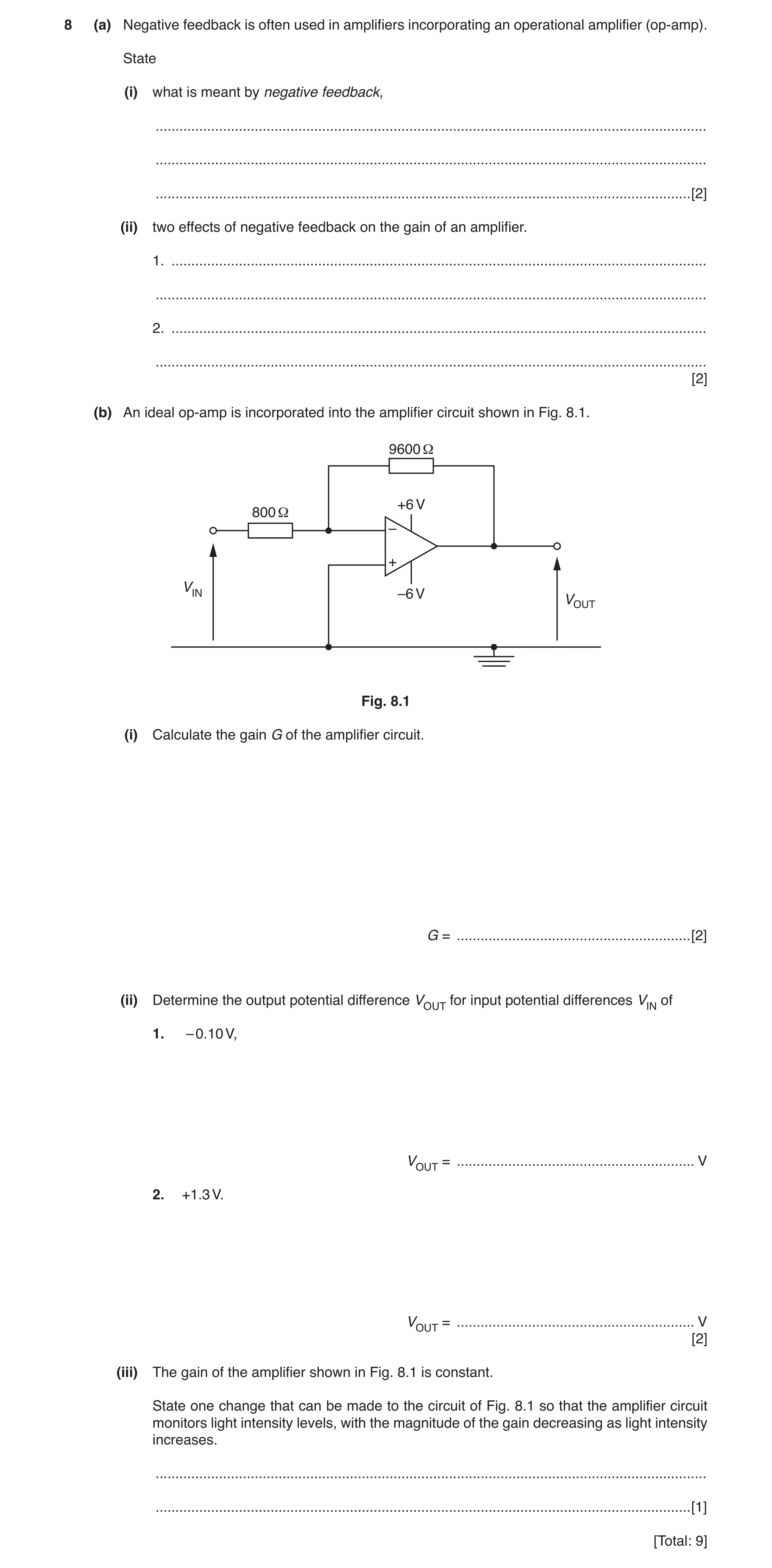
8 (a) Negative feedback is often used in amplifiers incorporating an operational amplifier (op-amp). State (i) what is meant by negative feedback, … … … [2] (ii) two effects of negative feedback on the gain of an amplifier. 1. … … 2. … … [2] (b) An ideal op-amp is incorporated into the amplifier circuit shown in Fig. 8.1. 9600 Ω +6 V 800 Ω – + VIN –6 V VOUT Fig. 8.1 (i) Calculate the gain G of the amplifier circuit. G = … [2] (ii) Determine the output potential difference VOUT for input potential differences VIN of 1. – 0.10 V, VOUT = … V 2. +1.3 V. VOUT = … V [2] (iii) The gain of the amplifier shown in Fig. 8.1 is constant. State one change that can be made to the circuit of Fig. 8.1 so that the amplifier circuit monitors light intensity levels, with the magnitude of the gain decreasing as light intensity increases. … … [1] [Total: 9]
9 marks
Mark scheme: 8(a)(i) (fraction of) output is combined with the input M1 output (fraction) subtracted/deducted from input A1 8(a)(ii) any two valid points e.g.: • greater bandwidth/gain constant over a larger range of frequencies/greater bandwidth • smaller gain B2 8(b)(i) gain = (–)9600 / 800 C1 = –12 A1 8(b)(ii) 1. 1.2 V B1 2. –6 V B1 8(b)(iii) replace the 9600 Ω resistor with an LDR B1
This question in 9702/41 May/June 2018
Q6 · Negative feedback is often used in amplifiers 9702/42 May/June 2018
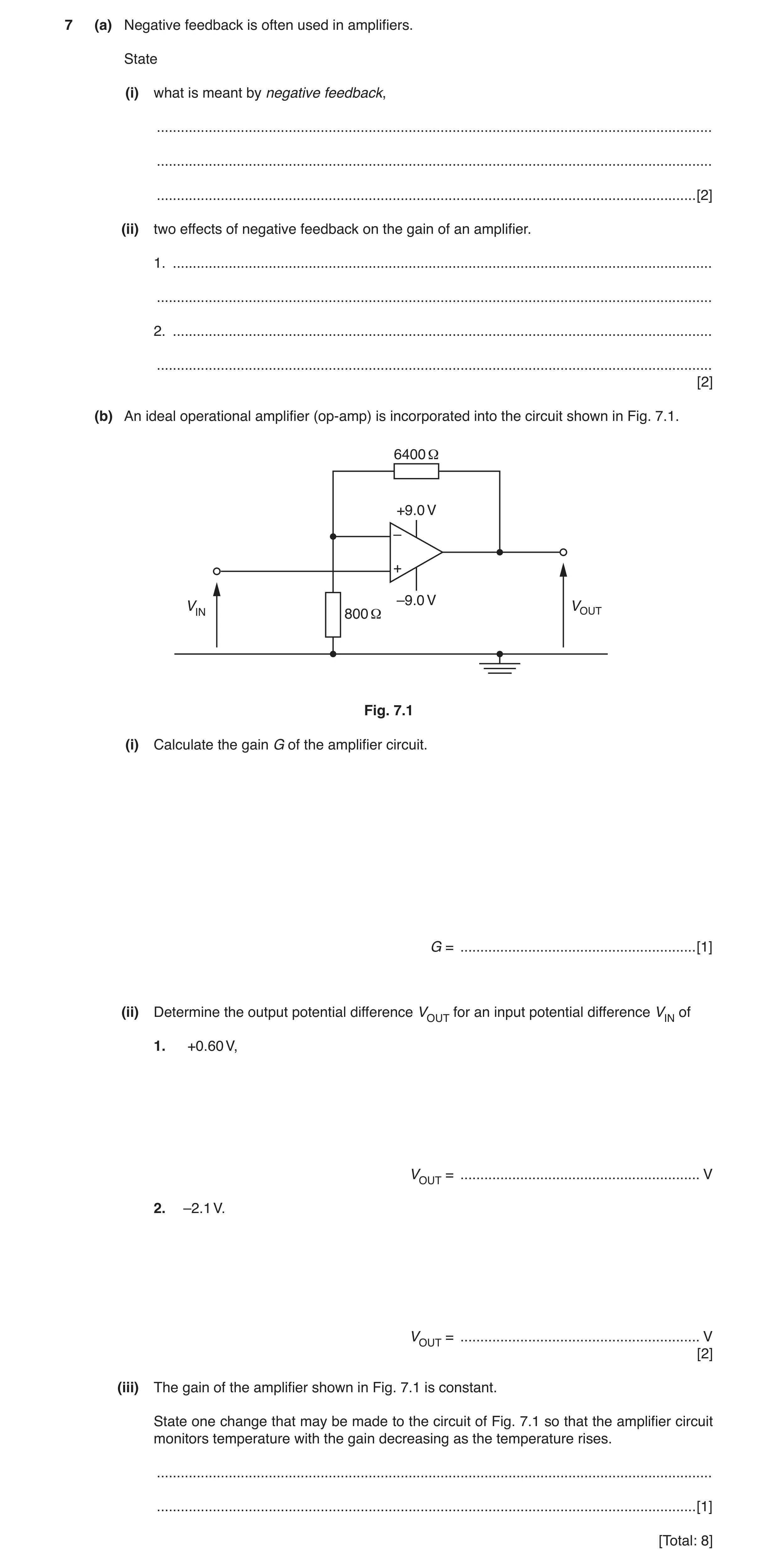
7 (a) Negative feedback is often used in amplifiers. State (i) what is meant by negative feedback, … … … [2] (ii) two effects of negative feedback on the gain of an amplifier. 1. … … 2. … … [2] (b) An ideal operational amplifier (op-amp) is incorporated into the circuit shown in Fig. 7.1. 6400 Ω +9.0 V – + –9.0 V VOUT VIN 800 Ω Fig. 7.1 (i) Calculate the gain G of the amplifier circuit. G = … [1] (ii) Determine the output potential difference VOUT for an input potential difference VIN of 1. +0.60 V, VOUT = … V 2. –2.1 V. VOUT = … V [2] (iii) The gain of the amplifier shown in Fig. 7.1 is constant. State one change that may be made to the circuit of Fig. 7.1 so that the amplifier circuit monitors temperature with the gain decreasing as the temperature rises. … … [1] [Total: 8]
8 marks
Mark scheme: 7(a)(i) (fraction of) output is combined with the input M1 output (fraction) subtracted/deducted from input A1 7(a)(ii) Any two valid points e.g. • greater bandwidth/gain constant over a larger range of frequencies • smaller gain B2 7(b)(i) gain = 1 + (6400 / 800) = 9.0 A1 7(b)(ii) 1. (+)5.4 V A1 2. –9.0 V A1 7(b)(iii) replace the 6400 Ω resistor with a thermistor B1
This question in 9702/42 May/June 2018
Q7 · Negative feedback is often used in amplifiers incorporating an operational amplifier… 9702/43 May/June 2018
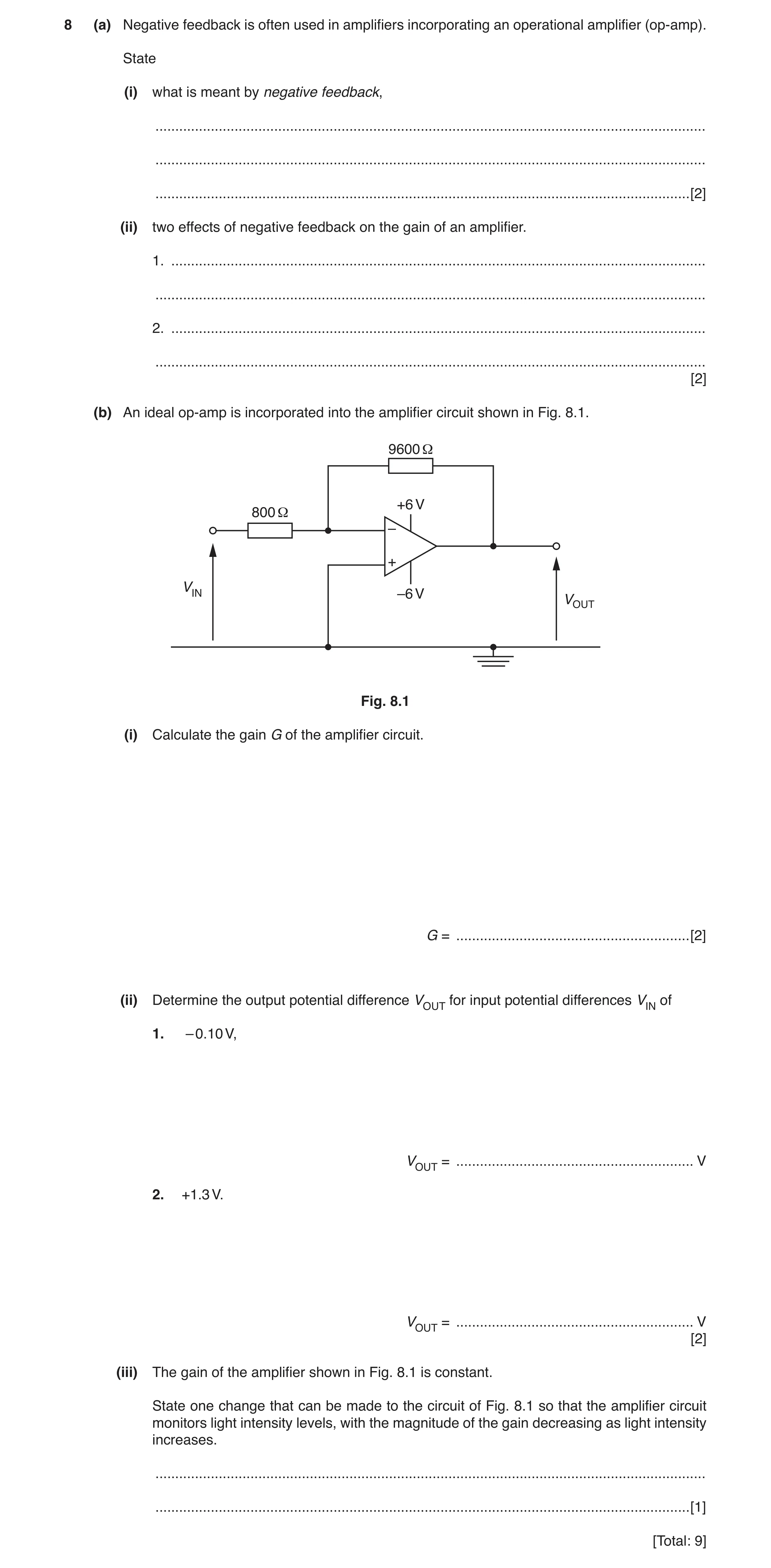
8 (a) Negative feedback is often used in amplifiers incorporating an operational amplifier (op-amp). State (i) what is meant by negative feedback, … … … [2] (ii) two effects of negative feedback on the gain of an amplifier. 1. … … 2. … … [2] (b) An ideal op-amp is incorporated into the amplifier circuit shown in Fig. 8.1. 9600 Ω +6 V 800 Ω – + VIN –6 V VOUT Fig. 8.1 (i) Calculate the gain G of the amplifier circuit. G = … [2] (ii) Determine the output potential difference VOUT for input potential differences VIN of 1. – 0.10 V, VOUT = … V 2. +1.3 V. VOUT = … V [2] (iii) The gain of the amplifier shown in Fig. 8.1 is constant. State one change that can be made to the circuit of Fig. 8.1 so that the amplifier circuit monitors light intensity levels, with the magnitude of the gain decreasing as light intensity increases. … … [1] [Total: 9]
9 marks
Mark scheme: 8(a)(i) (fraction of) output is combined with the input M1 output (fraction) subtracted/deducted from input A1 8(a)(ii) any two valid points e.g.: • greater bandwidth/gain constant over a larger range of frequencies/greater bandwidth • smaller gain B2 8(b)(i) gain = (–)9600 / 800 C1 = –12 A1 8(b)(ii) 1. 1.2 V B1 2. –6 V B1 8(b)(iii) replace the 9600 Ω resistor with an LDR B1
This question in 9702/43 May/June 2018
Q8 · An ideal operational amplifier (op-amp) has infinite bandwidth and infinite slew rate 9702/41 Oct/Nov 2018
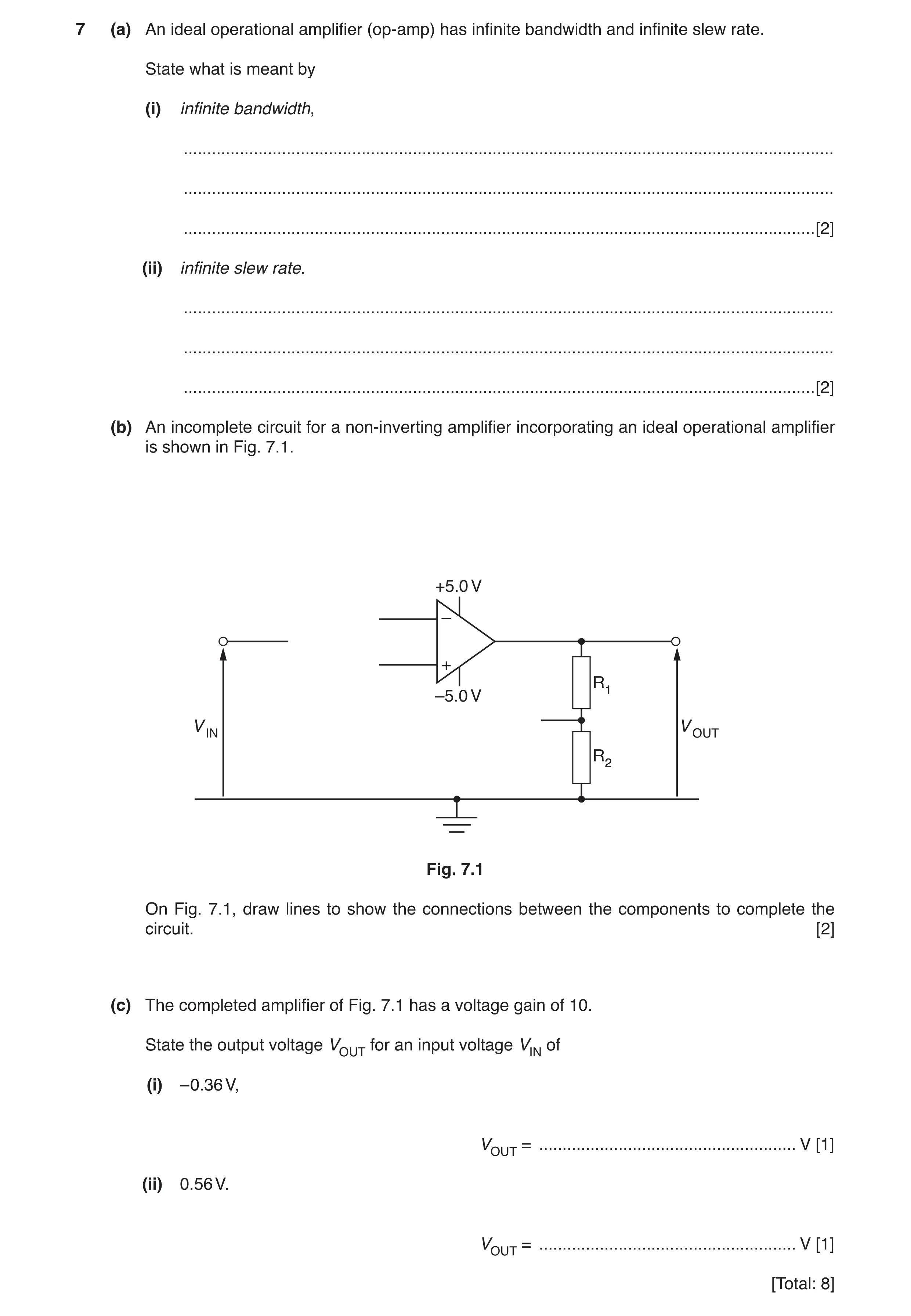
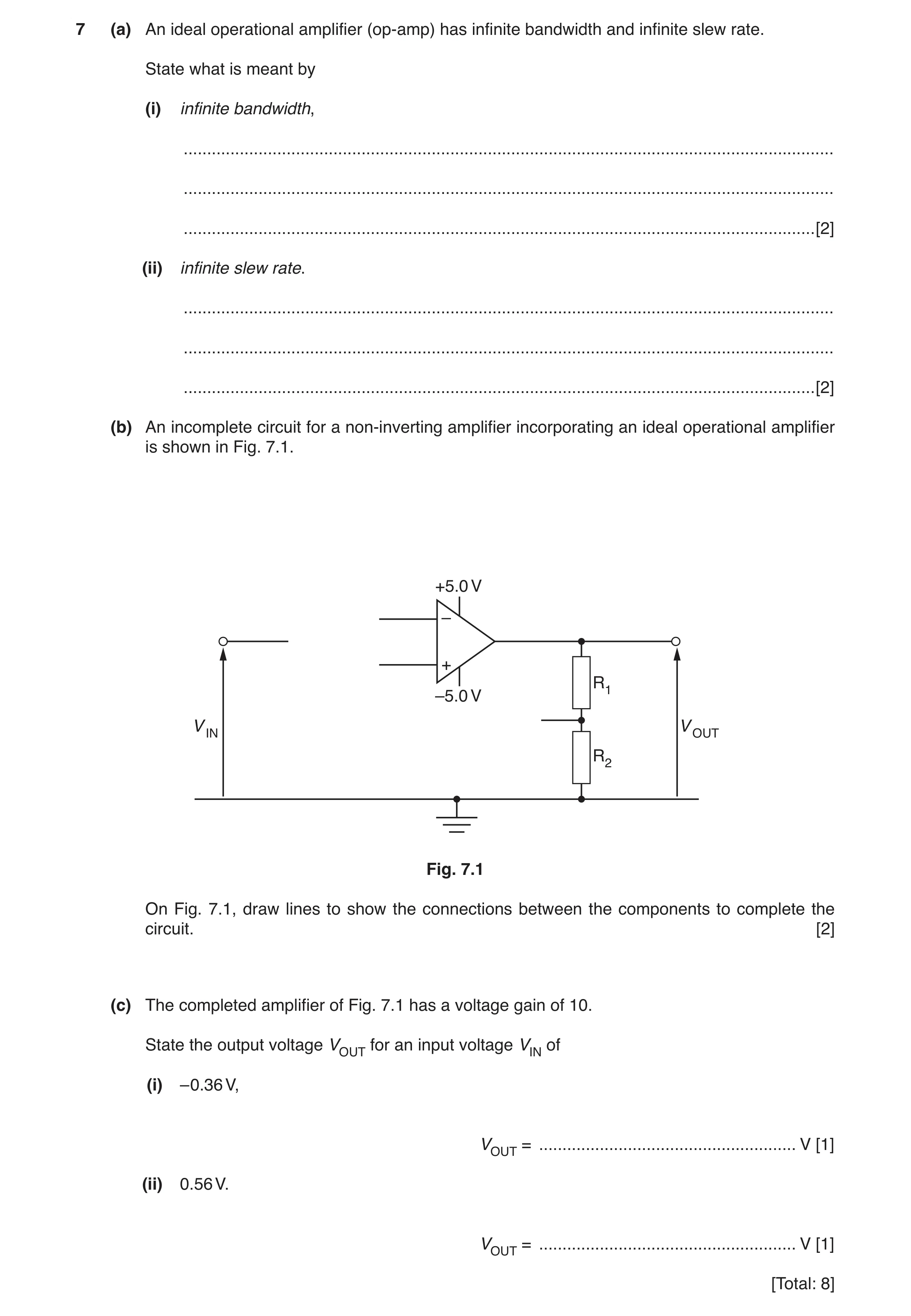
7 (a) An ideal operational amplifier (op-amp) has infinite bandwidth and infinite slew rate. State what is meant by (i) infinite bandwidth, … … … [2] (ii) infinite slew rate. … … … [2] (b) An incomplete circuit for a non-inverting amplifier incorporating an ideal operational amplifier is shown in Fig. 7.1. +5.0 V – + R1 –5.0 V V IN V OUT R2 Fig. 7.1 On Fig. 7.1, draw lines to show the connections between the components to complete the circuit. [2] (c) The completed amplifier of Fig. 7.1 has a voltage gain of 10. State the output voltage VOUT for an input voltage VIN of (i) –0.36 V, VOUT = … V [1] (ii) 0.56 V. VOUT = … V [1] [Total: 8]
8 marks
Mark scheme: 7(a)(i) gain is constant M1 for all frequencies A1 7(a)(ii) no time delay between input (voltage) and output (voltage) B1 clear reference to change(s) in input and/or output (voltages) B1 7(b) diagram: VIN connected to V+ only B1 midpoint between resistors R1 and R2 connected to V– only B1 7(c)(i) –3.6 V A1 7(c)(ii) (+)5.0 V A1
This question in 9702/41 Oct/Nov 2018
Q9 · A circuit incorporating an ideal operational amplifier (op-amp) is shown in Fig 9702/42 Oct/Nov 2018
7 A circuit incorporating an ideal operational amplifier (op-amp) is shown in Fig. 7.1. +5.0 V +5.0 V RT 1.8 kΩ – + –5.0 V VOUT R 2.4 kΩ Fig. 7.1 The variation with temperature θ of the resistance RT of the thermistor is shown in Fig. 7.2. 3.4 3.3 Ω RT / k 3.2 3.1 3.0 2 3 4 5 6 7 θ / °C Fig. 7.2 (a) The output potential VOUT of the op-amp circuit changes sign when the temperature of the thermistor is 4.0 °C. Calculate the resistance R. R = … kΩ [2] (b) State and explain whether the output potential VOUT is +5.0 V or −5.0 V for a thermistor temperature of 2.5 °C. … … … … [3] (c) The output of the op-amp is to be displayed using two light-emitting diodes (LEDs) labelled G and B. When the temperature of the thermistor is below 4.0 °C, only the LED labelled G emits light. The LED labelled B emits light only when the temperature of the thermistor is above 4.0 °C. On Fig. 7.1, draw and label the symbols for the two LEDs. [3] [Total: 8]
8 marks
Mark scheme: 7(a) R / RT = 2.4 / 1.8 or at 4.0 °C, RT = 3.2 kΩ C1 hence R / 3.2 = 2.4 / 1.8 R = 4.3 kΩ A1 7(b) RT = 3.37 kΩ or RT is greater (than 3.2 kΩ) B1 V+ > V– M1 hence output is +5.0 V A1 Question Answer Marks 7(c) correct LED symbol B1 two diodes shown connected, in parallel and with opposite polarities, between VOUT and earth M1 diodes labelled to show correct polarities consistent with (b) (G pointing from VOUT to earth and B pointing from earth to VOUT if (b) correct) A1
This question in 9702/42 Oct/Nov 2018
Q10 · An ideal operational amplifier (op-amp) has infinite bandwidth and infinite slew rate 9702/43 Oct/Nov 2018
7 (a) An ideal operational amplifier (op-amp) has infinite bandwidth and infinite slew rate. State what is meant by (i) infinite bandwidth, … … … [2] (ii) infinite slew rate. … … … [2] (b) An incomplete circuit for a non-inverting amplifier incorporating an ideal operational amplifier is shown in Fig. 7.1. +5.0 V – + R1 –5.0 V V IN V OUT R2 Fig. 7.1 On Fig. 7.1, draw lines to show the connections between the components to complete the circuit. [2] (c) The completed amplifier of Fig. 7.1 has a voltage gain of 10. State the output voltage VOUT for an input voltage VIN of (i) –0.36 V, VOUT = … V [1] (ii) 0.56 V. VOUT = … V [1] [Total: 8]
8 marks
Mark scheme: 7(a)(i) gain is constant M1 for all frequencies A1 7(a)(ii) no time delay between input (voltage) and output (voltage) B1 clear reference to change(s) in input and/or output (voltages) B1 7(b) diagram: VIN connected to V+ only B1 midpoint between resistors R1 and R2 connected to V– only B1 7(c)(i) –3.6 V A1 7(c)(ii) (+)5.0 V A1
This question in 9702/43 Oct/Nov 2018
Q11 · Two properties that an ideal operational amplifier (op-amp) would have are constant… 9702/42 Feb/March 2019
7 (a) Two properties that an ideal operational amplifier (op-amp) would have are constant voltage gain and infinite slew rate. State what is meant by: (i) gain of an amplifier … … [1] (ii) infinite slew rate. … … … [2] (b) The partially completed circuit of a non-inverting amplifier, incorporating an ideal op-amp, is shown in Fig. 7.1. R1 +9 V + – VIN –9 V VOUT R2 Fig. 7.1 (i) On Fig. 7.1, complete the circuit for the non-inverting amplifier. [2] (ii) For the completed circuit of Fig. 7.1, the gain of the amplifier is 25. The resistance of resistor R1 is 12 kΩ. Calculate the resistance of resistor R2. resistance = … Ω [2] (iii) Calculate, for the amplifier gain of 25, the range of values of VIN for which the amplifier does not saturate. range from … V to … V [2] [Total: 9]
9 marks
Mark scheme: 7(a)(i) output voltage / input voltage B1 7(a)(ii) no time delay between input and output B1 clear reference to change(s) in input and / or output B1 7(b)(i) VIN only connected to non-inverting input B1 midpoint between R1 and R2 only connected to inverting input B1 Question Answer Marks 7(b)(ii) gain = 1 + (R1 / R2) 25 = 1 + (12 × 103) / R2 C1 R2 = 500 Ω A1 7(b)(iii) VMAX = 9/25 = 0.36 V C1 range is –0.36 V to + 0.36 V A1
This question in 9702/42 Feb/March 2019
Q12 · The circuit for an inverting amplifier incorporating an ideal operational amplifier… 9702/41 May/June 2019
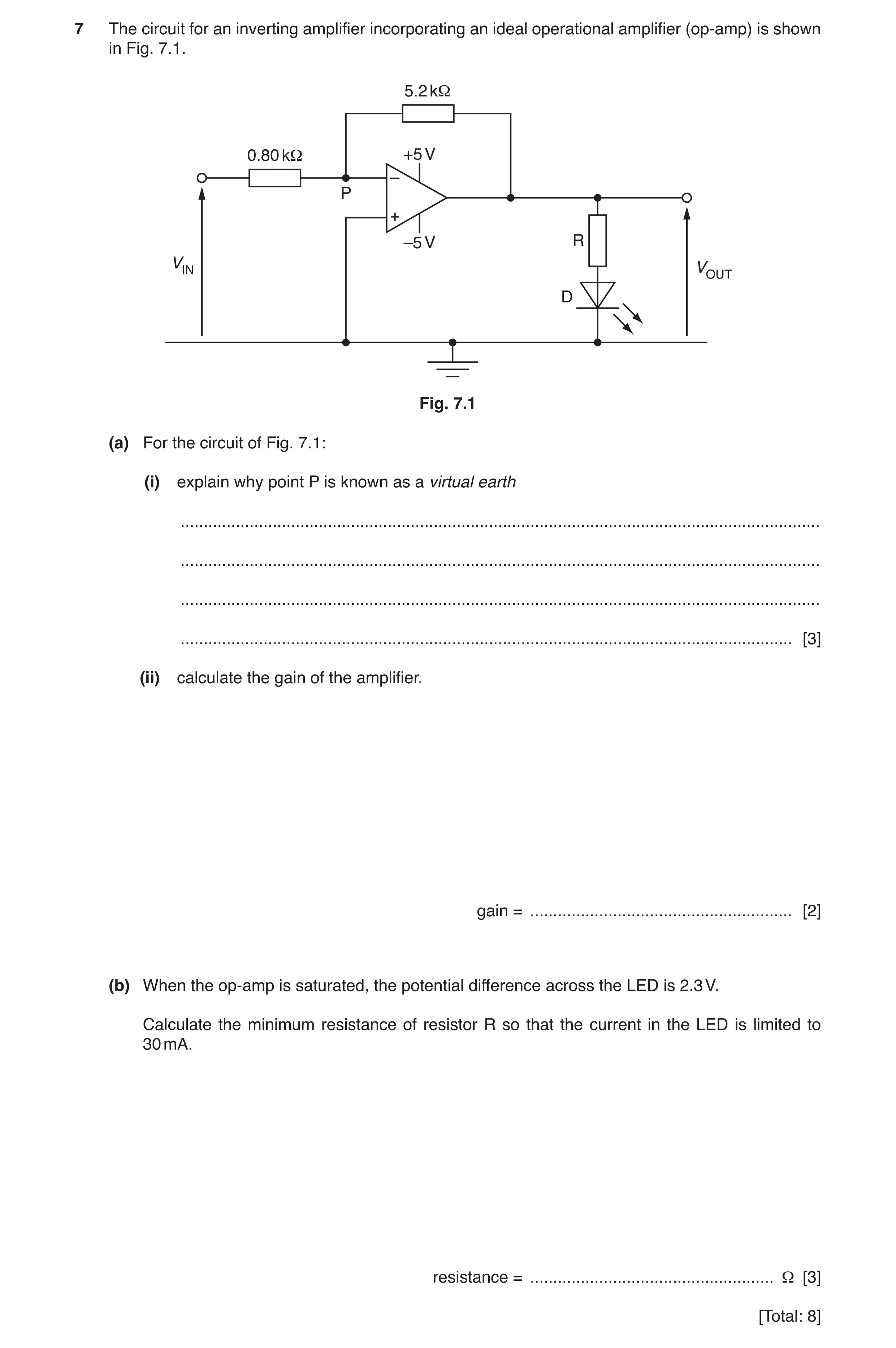
7 The circuit for an inverting amplifier incorporating an ideal operational amplifier (op-amp) is shown in Fig. 7.1. 5.2 k 0.80 k +5 V – P + –5 V R VIN VOUT D Fig. 7.1 (a) For the circuit of Fig. 7.1: (i) explain why point P is known as a virtual earth … … … … [3] (ii) calculate the gain of the amplifier. gain = … [2] (b) When the op-amp is saturated, the potential difference across the LED is 2.3 V. Calculate the minimum resistance of resistor R so that the current in the LED is limited to 30 mA. resistance = … Ω [3] [Total: 8]
8 marks
Mark scheme: 7(a)(i) (amplifier) gain is very large/infinite B1 for amplifier not to saturate, V+ = V– or feedback (loop) ensures V+ = V– B1 V+ is at earth/0 V so V– is (almost) at earth/0 V B1 7(a)(ii) gain = (–)5200 / 800 or (–)5.2 / 0.80 C1 = –6.5 A1 Question Answer Marks 7(b) (at saturation,) VOUT = 5 V C1 p.d. across R = 5 – 2.3 = 2.7 (V) C1 resistance = 2.7 / (30 × 10–3) = 90 Ω A1 or Rdiode = 2.3 / 0.030 = 77 Ω Rtotal = 5.0 / 0.030 = 167 Ω (C1) Rresistor (= 167 – 77) = 90 Ω (A1) or Rdiode = 2.3 / 0.030 = 77 Ω 77 / (Rresistor + 77) × 5 = 2.3 (C1) Rresistor = 90 Ω (A1) or Rdiode = 2.3 / 0.030 = 77 Ω Rresistor = 77 × (2.7 / 2.3) (C1) Rresistor = 90 Ω (A1)
This question in 9702/41 May/June 2019
Q13 · Part of a circuit incorporating an operational amplifier (op-amp) is shown in Fig 9702/42 May/June 2019
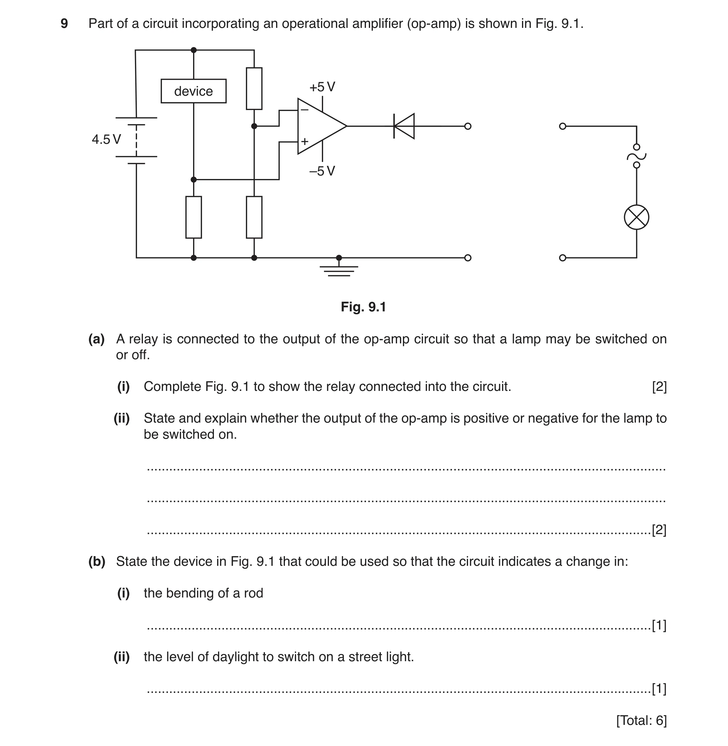
9 Part of a circuit incorporating an operational amplifier (op-amp) is shown in Fig. 9.1. +5 V device – 4.5 V + –5 V Fig. 9.1 (a) A relay is connected to the output of the op-amp circuit so that a lamp may be switched on or off. (i) Complete Fig. 9.1 to show the relay connected into the circuit. [2] (ii) State and explain whether the output of the op-amp is positive or negative for the lamp to be switched on. … … … [2] (b) State the device in Fig. 9.1 that could be used so that the circuit indicates a change in: (i) the bending of a rod … [1] (ii) the level of daylight to switch on a street light. … [1] [Total: 6]
6 marks
Mark scheme: 9(a)(i) relay coil shown connected between diode and earth B1 switch shown connected across lamp B1 9(a)(ii) Any one from: • (for diode to conduct) current flow is into output of op-amp • when earth is at higher potential diode is forward biased • diode blocks current when output positive • diode must conduct M1 so VOUT is negative A1 9(b)(i) strain gauge B1 9(b)(ii) light-dependent resistor B1
This question in 9702/42 May/June 2019
Q14 · The circuit for an inverting amplifier incorporating an ideal operational amplifier… 9702/43 May/June 2019
7 The circuit for an inverting amplifier incorporating an ideal operational amplifier (op-amp) is shown in Fig. 7.1. 5.2 k 0.80 k +5 V – P + –5 V R VIN VOUT D Fig. 7.1 (a) For the circuit of Fig. 7.1: (i) explain why point P is known as a virtual earth … … … … [3] (ii) calculate the gain of the amplifier. gain = … [2] (b) When the op-amp is saturated, the potential difference across the LED is 2.3 V. Calculate the minimum resistance of resistor R so that the current in the LED is limited to 30 mA. resistance = … Ω [3] [Total: 8]
8 marks
Mark scheme: 7(a)(i) (amplifier) gain is very large/infinite B1 for amplifier not to saturate, V+ = V– or feedback (loop) ensures V+ = V– B1 V+ is at earth/0 V so V– is (almost) at earth/0 V B1 7(a)(ii) gain = (–)5200 / 800 or (–)5.2 / 0.80 C1 = –6.5 A1 Question Answer Marks 7(b) (at saturation,) VOUT = 5 V C1 p.d. across R = 5 – 2.3 = 2.7 (V) C1 resistance = 2.7 / (30 × 10–3) = 90 Ω A1 or Rdiode = 2.3 / 0.030 = 77 Ω Rtotal = 5.0 / 0.030 = 167 Ω (C1) Rresistor (= 167 – 77) = 90 Ω (A1) or Rdiode = 2.3 / 0.030 = 77 Ω 77 / (Rresistor + 77) × 5 = 2.3 (C1) Rresistor = 90 Ω (A1) or Rdiode = 2.3 / 0.030 = 77 Ω Rresistor = 77 × (2.7 / 2.3) (C1) Rresistor = 90 Ω (A1)
This question in 9702/43 May/June 2019
Q15 · A section of a coaxial cable is shown in Fig 9702/41 Oct/Nov 2019
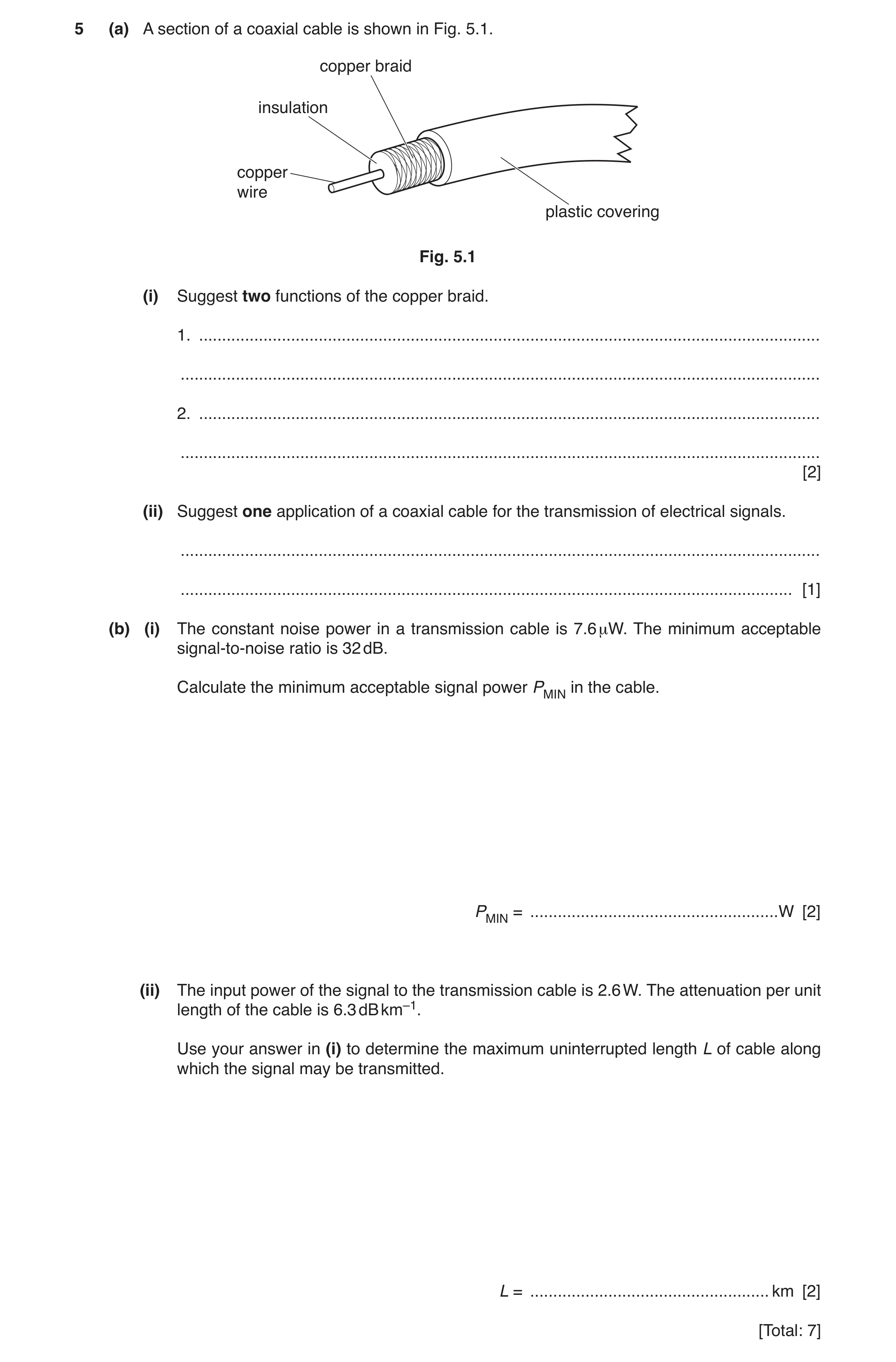
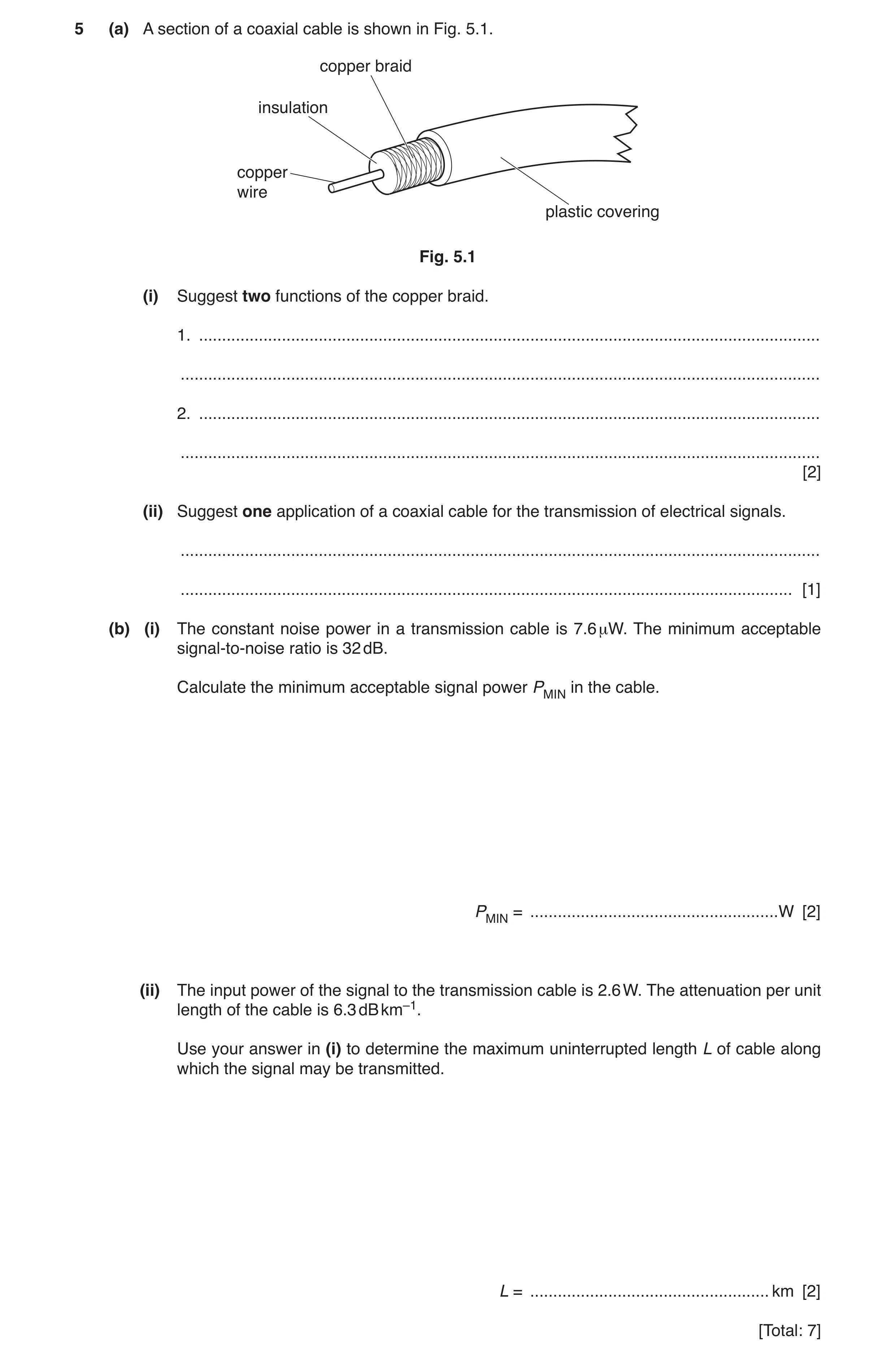
5 (a) A section of a coaxial cable is shown in Fig. 5.1. copper braid insulation copper wire plastic covering Fig. 5.1 (i) Suggest two functions of the copper braid. 1. … … 2. … … [2] (ii) Suggest one application of a coaxial cable for the transmission of electrical signals. … … [1] (b) (i) The constant noise power in a transmission cable is 7.6 μW. The minimum acceptable signal-to-noise ratio is 32 dB. Calculate the minimum acceptable signal power PMIN in the cable. PMIN = … W [2] (ii) The input power of the signal to the transmission cable is 2.6 W. The attenuation per unit length of the cable is 6.3 dB km–1. Use your answer in (i) to determine the maximum uninterrupted length L of cable along which the signal may be transmitted. L = … km [2] [Total: 7]
7 marks
Mark scheme: 5(a)(i) provides return for the signal B1 shields signal from noise B1 5(a)(ii) e.g. connection between aerial and TV set B1 5(b)(i) gain / dB = 10 lg (P1 / P2) C1 32 = 10 lg {PMIN / (7.6 × 10⁻⁶)} PMIN = 0.012 W A1 5(b)(ii) attenuation per unit length = (1 / L) × 10 lg (P1 / P2) 6.3 = (1 / L) × 10 lg (2.6 / 0.012) C1 L = 3.7 km A1
This question in 9702/41 Oct/Nov 2019
Q16 · An ideal operational amplifier (op-amp) has infinite bandwidth and zero output impedance 9702/41 Oct/Nov 2019
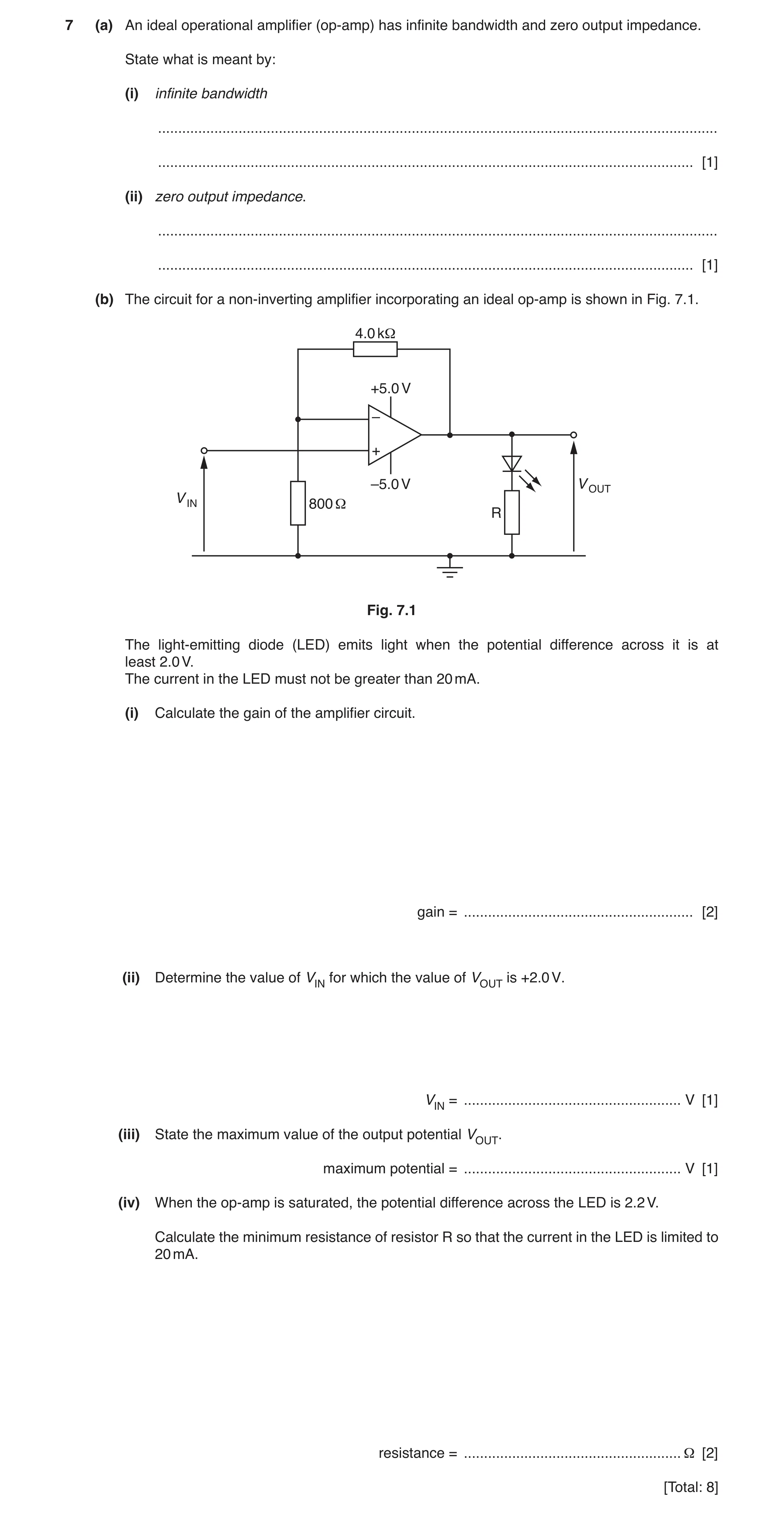
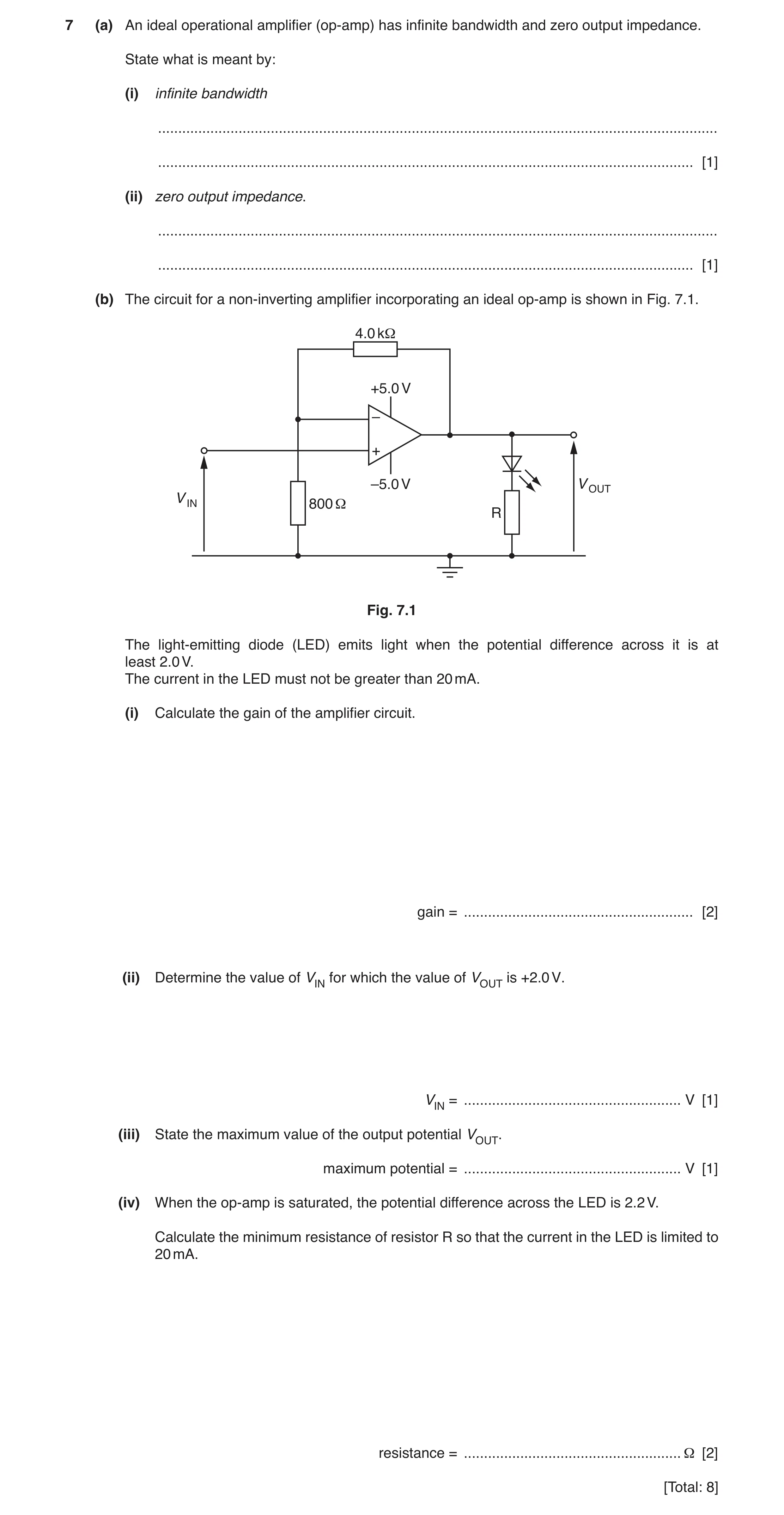
7 (a) An ideal operational amplifier (op-amp) has infinite bandwidth and zero output impedance. State what is meant by: (i) infinite bandwidth … … [1] (ii) zero output impedance. … … [1] (b) The circuit for a non-inverting amplifier incorporating an ideal op-amp is shown in Fig. 7.1. 4.0 kΩ +5.0 V – + –5.0 V V OUT V IN 800 Ω R Fig. 7.1 The light-emitting diode (LED) emits light when the potential difference across it is at least 2.0 V. The current in the LED must not be greater than 20 mA. (i) Calculate the gain of the amplifier circuit. gain = … [2] (ii) Determine the value of VIN for which the value of VOUT is +2.0 V. VIN = … V [1] (iii) State the maximum value of the output potential VOUT. maximum potential = … V [1] (iv) When the op-amp is saturated, the potential difference across the LED is 2.2 V. Calculate the minimum resistance of resistor R so that the current in the LED is limited to 20 mA. resistance = … Ω [2] [Total: 8]
8 marks
Mark scheme: 7(a)(i) all frequencies are amplified equally B1 7(a)(ii) no drop in output voltage (when there is a current) B1 7(b)(i) gain = 1 + RF / RIN gain = 1 + (4000 / 800) C1 gain = 6.0 A1 7(b)(ii) 2.0 / VIN = 6.0 VIN = (+)0.33 V A1 7(b)(iii) 5.0 V A1 7(b)(iv) V = 5.0 – 2.2 (= 2.8 V) C1 R = V / I = 2.8 / 0.020 = 140 Ω A1
This question in 9702/41 Oct/Nov 2019
Q17 · A section of a coaxial cable is shown in Fig 9702/43 Oct/Nov 2019
5 (a) A section of a coaxial cable is shown in Fig. 5.1. copper braid insulation copper wire plastic covering Fig. 5.1 (i) Suggest two functions of the copper braid. 1. … … 2. … … [2] (ii) Suggest one application of a coaxial cable for the transmission of electrical signals. … … [1] (b) (i) The constant noise power in a transmission cable is 7.6 μW. The minimum acceptable signal-to-noise ratio is 32 dB. Calculate the minimum acceptable signal power PMIN in the cable. PMIN = … W [2] (ii) The input power of the signal to the transmission cable is 2.6 W. The attenuation per unit length of the cable is 6.3 dB km–1. Use your answer in (i) to determine the maximum uninterrupted length L of cable along which the signal may be transmitted. L = … km [2] [Total: 7]
7 marks
Mark scheme: 5(a)(i) provides return for the signal B1 shields signal from noise B1 5(a)(ii) e.g. connection between aerial and TV set B1 5(b)(i) gain / dB = 10 lg (P1 / P2) C1 32 = 10 lg {PMIN / (7.6 × 10⁻⁶)} PMIN = 0.012 W A1 5(b)(ii) attenuation per unit length = (1 / L) × 10 lg (P1 / P2) 6.3 = (1 / L) × 10 lg (2.6 / 0.012) C1 L = 3.7 km A1
This question in 9702/43 Oct/Nov 2019
Q18 · An ideal operational amplifier (op-amp) has infinite bandwidth and zero output impedance 9702/43 Oct/Nov 2019
7 (a) An ideal operational amplifier (op-amp) has infinite bandwidth and zero output impedance. State what is meant by: (i) infinite bandwidth … … [1] (ii) zero output impedance. … … [1] (b) The circuit for a non-inverting amplifier incorporating an ideal op-amp is shown in Fig. 7.1. 4.0 kΩ +5.0 V – + –5.0 V V OUT V IN 800 Ω R Fig. 7.1 The light-emitting diode (LED) emits light when the potential difference across it is at least 2.0 V. The current in the LED must not be greater than 20 mA. (i) Calculate the gain of the amplifier circuit. gain = … [2] (ii) Determine the value of VIN for which the value of VOUT is +2.0 V. VIN = … V [1] (iii) State the maximum value of the output potential VOUT. maximum potential = … V [1] (iv) When the op-amp is saturated, the potential difference across the LED is 2.2 V. Calculate the minimum resistance of resistor R so that the current in the LED is limited to 20 mA. resistance = … Ω [2] [Total: 8]
8 marks
Mark scheme: 7(a)(i) all frequencies are amplified equally B1 7(a)(ii) no drop in output voltage (when there is a current) B1 7(b)(i) gain = 1 + RF / RIN gain = 1 + (4000 / 800) C1 gain = 6.0 A1 7(b)(ii) 2.0 / VIN = 6.0 VIN = (+)0.33 V A1 7(b)(iii) 5.0 V A1 7(b)(iv) V = 5.0 – 2.2 (= 2.8 V) C1 R = V / I = 2.8 / 0.020 = 140 Ω A1
This question in 9702/43 Oct/Nov 2019
Q19 · An ideal operational amplifier (op‑amp) is connected to a load resistor 9702/42 May/June 2020
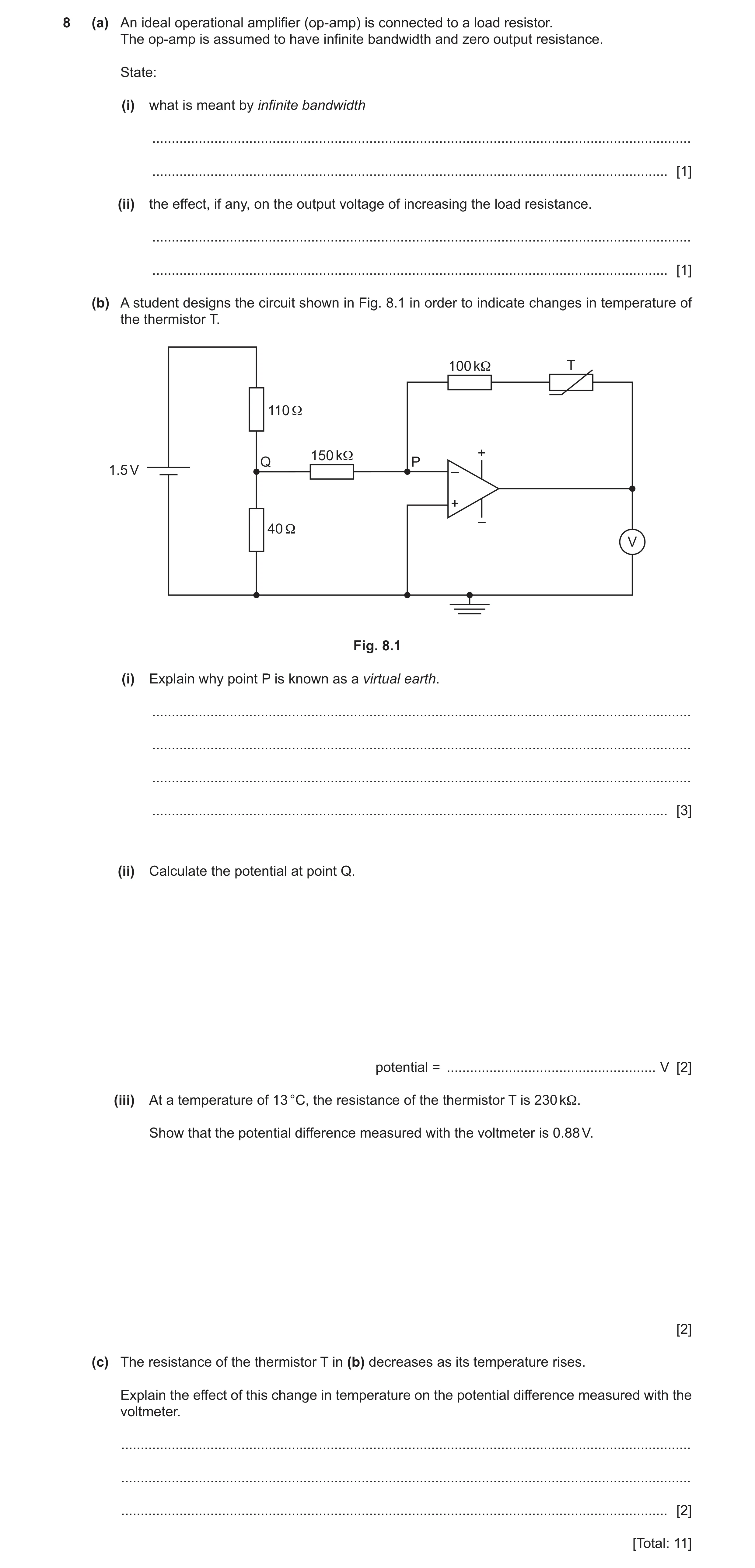
8 (a) An ideal operational amplifier (op‑amp) is connected to a load resistor. The op‑amp is assumed to have infinite bandwidth and zero output resistance. State: (i) what is meant by infinite bandwidth … … [1] (ii) the effect, if any, on the output voltage of increasing the load resistance. … … [1] (b) A student designs the circuit shown in Fig. 8.1 in order to indicate changes in temperature of the thermistor T. 100 kΩ T 110 Ω 150 kΩ + Q P 1.5 V – + – 40 Ω V Fig. 8.1 (i) Explain why point P is known as a virtual earth. … … … … [3] (ii) Calculate the potential at point Q. potential = … V [2] (iii) At a temperature of 13 °C, the resistance of the thermistor T is 230 kΩ. Show that the potential difference measured with the voltmeter is 0.88 V. [2] (c) The resistance of the thermistor T in (b) decreases as its temperature rises. Explain the effect of this change in temperature on the potential difference measured with the voltmeter. … … … [2] [Total: 11]
11 marks
Mark scheme: 8(a)(i) constant gain for all frequencies B1 8(a)(ii) unchanged B1 8(b)(i) (open loop) gain of op-amp is infinite B1 feedback loop ensures V+ ≈ V– or any difference between V+ and V– results in saturated output B1 non-inverting input is 0 V so inverting input also at 0 V B1 8(b)(ii) input = (40 × 1.5) / (40 + 110) C1 = 0.40 V A1 8(b)(iii) gain = (–) (100 + 230) / 150 or feedback current = 0.40 / (150 × 103) (A) C1 p.d. = [(100 + 230) / 150] × 0.40 = 0.88 V A1 8(c) (magnitude of) gain decreases M1 voltmeter reading decreases A1
This question in 9702/42 May/June 2020
Q20 · An ideal operational amplifier (op-amp) is said to have infinite bandwidth and infinite… 9702/42 Oct/Nov 2020
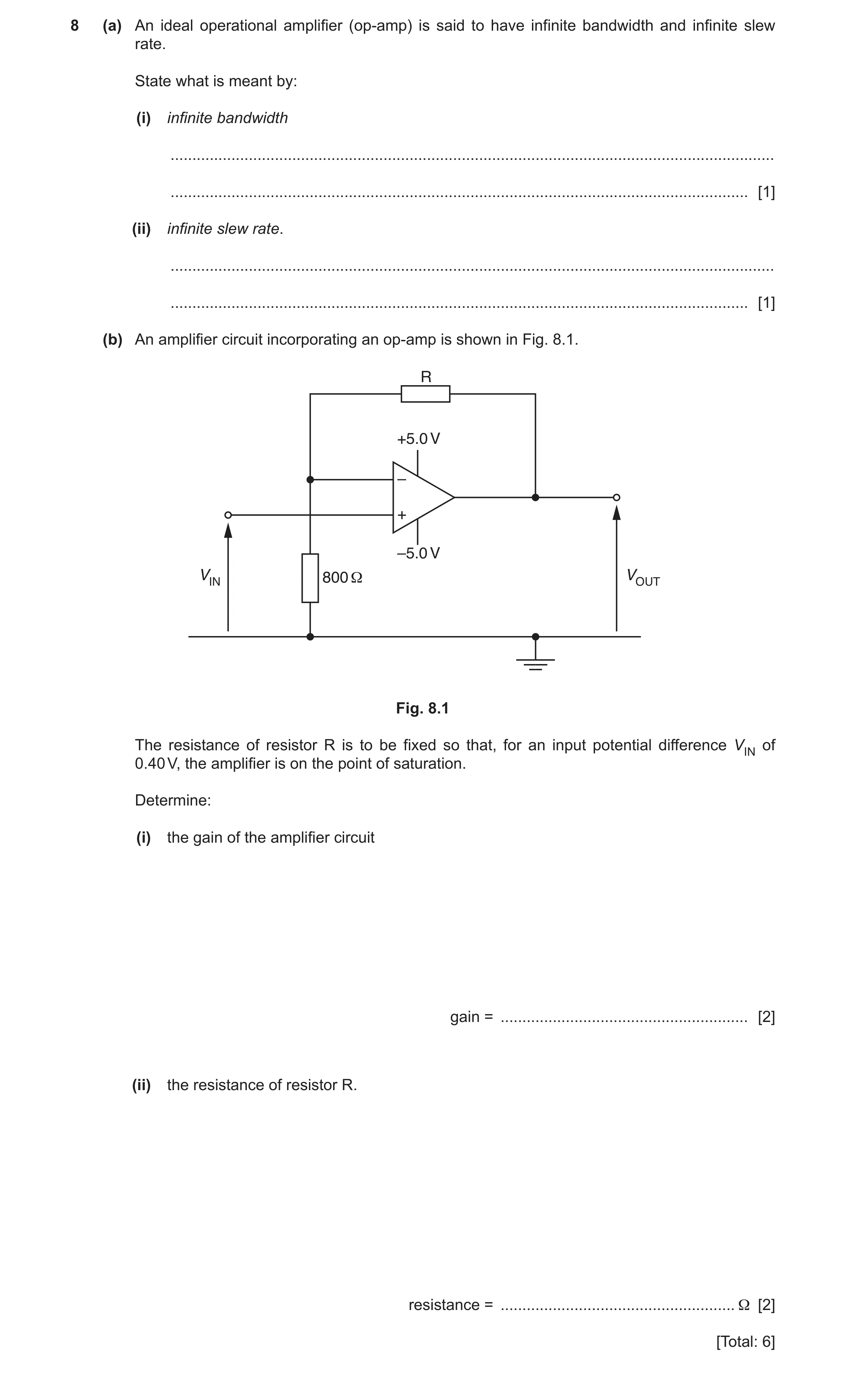
8 (a) An ideal operational amplifier (op-amp) is said to have infinite bandwidth and infinite slew rate. State what is meant by: (i) infinite bandwidth … … [1] (ii) infinite slew rate. … … [1] (b) An amplifier circuit incorporating an op-amp is shown in Fig. 8.1. R +5.0 V – + –5.0 V VIN 800 Ω VOUT Fig. 8.1 The resistance of resistor R is to be fixed so that, for an input potential difference VIN of 0.40 V, the amplifier is on the point of saturation. Determine: (i) the gain of the amplifier circuit gain = … [2] (ii) the resistance of resistor R. resistance = … Ω [2] [Total: 6]
6 marks
Mark scheme: 8(a)(i) gain is the same for all frequencies B1 8(a)(ii) no (time) delay in change in output when input is changed B1 8(b)(i) (at saturation,) VOUT = 5.0 V C1 gain = 5.0 / 0.40 = 12.5 or 13 A1 8(b)(ii) 12.5 = 1 + (R / 800) C1 R = 9200 Ω A1
This question in 9702/42 Oct/Nov 2020
Q21 · The circuit diagram containing an operational amplifier (op-amp) 9702/42 Feb/March 2021
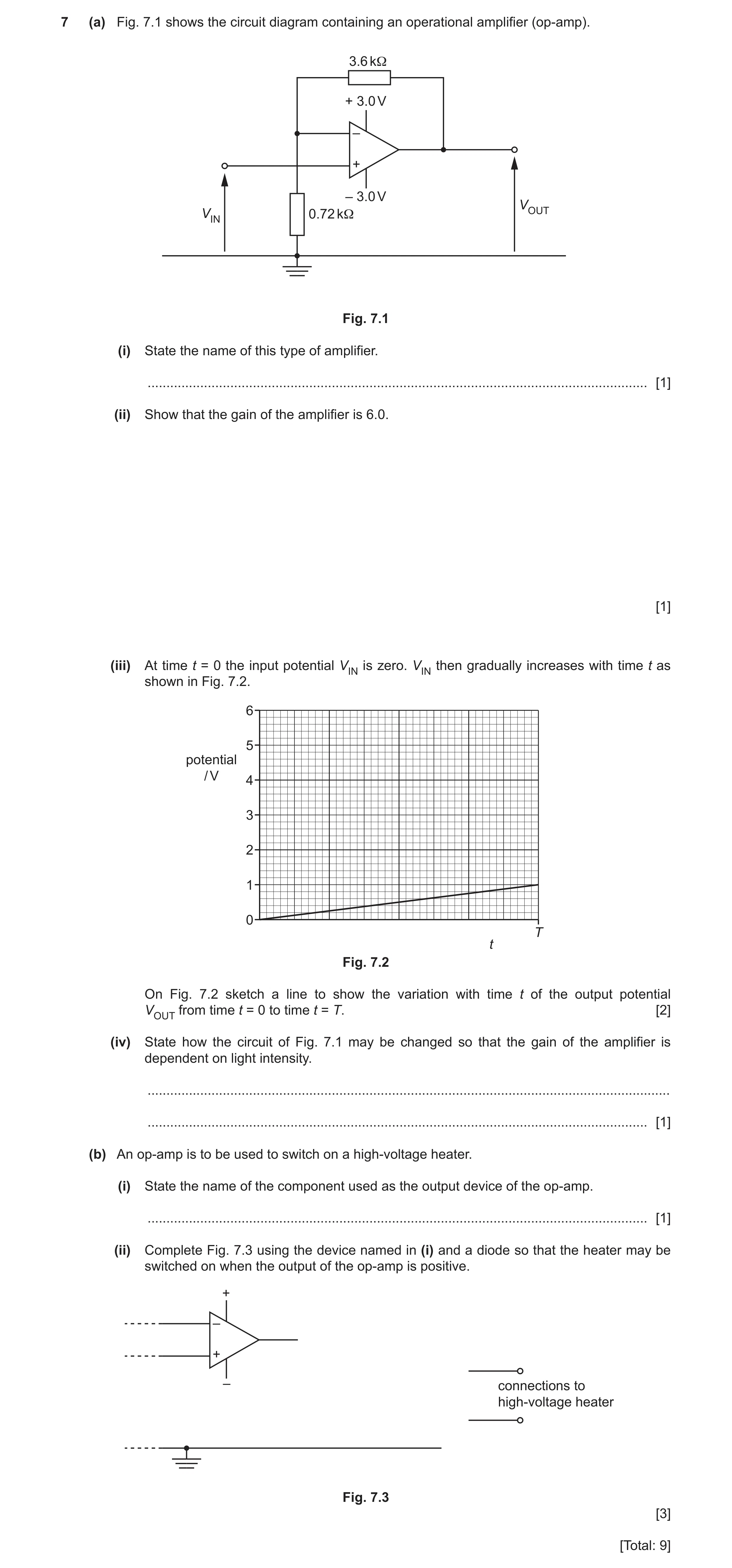
7 (a) Fig. 7.1 shows the circuit diagram containing an operational amplifier (op-amp). 3.6 kΩ + 3.0 V – + – 3.0 V VOUT VIN 0.72 kΩ Fig. 7.1 (i) State the name of this type of amplifier. … [1] (ii) Show that the gain of the amplifier is 6.0. [1] (iii) At time t = 0 the input potential VIN is zero. VIN then gradually increases with time t as shown in Fig. 7.2. 6 5 potential / V 4 3 2 1 0 T t Fig. 7.2 On Fig. 7.2 sketch a line to show the variation with time t of the output potential VOUT from time t = 0 to time t = T. [2] (iv) State how the circuit of Fig. 7.1 may be changed so that the gain of the amplifier is dependent on light intensity. … … [1] (b) An op-amp is to be used to switch on a high-voltage heater. (i) State the name of the component used as the output device of the op-amp. … [1] (ii) Complete Fig. 7.3 using the device named in (i) and a diode so that the heater may be switched on when the output of the op-amp is positive. + – + – connections to high-voltage heater Fig. 7.3 [3] [Total: 9]
9 marks
Mark scheme: 7(a)(i) non-inverting (amplifier) B1 7(a)(ii) gain 1 f R R = + 3.6 gain 1 6.0 0.72 = + = B1 7(a)(iii) straight line from (0,0) to (T / 2, 3) B1 line from origin to 3.0 V then horizontal line at 3.0 V to T B1 7(a)(iv) ldr / light dependent resistor replaces one of the two resistors B1 7(b)(i) relay coil B1 7(b)(ii) relay coil between op-amp and earth B1 diode with correct polarity (pointing away from output) connected between output and device and no other connections or diode with correct polarity (pointing towards earth) between device and earth and no other connections B1 switch connected to high voltage circuit B1
This question in 9702/42 Feb/March 2021
Q22 · Two properties of an ideal operational amplifier (op-amp) are infinite input impedance… 9702/42 May/June 2021
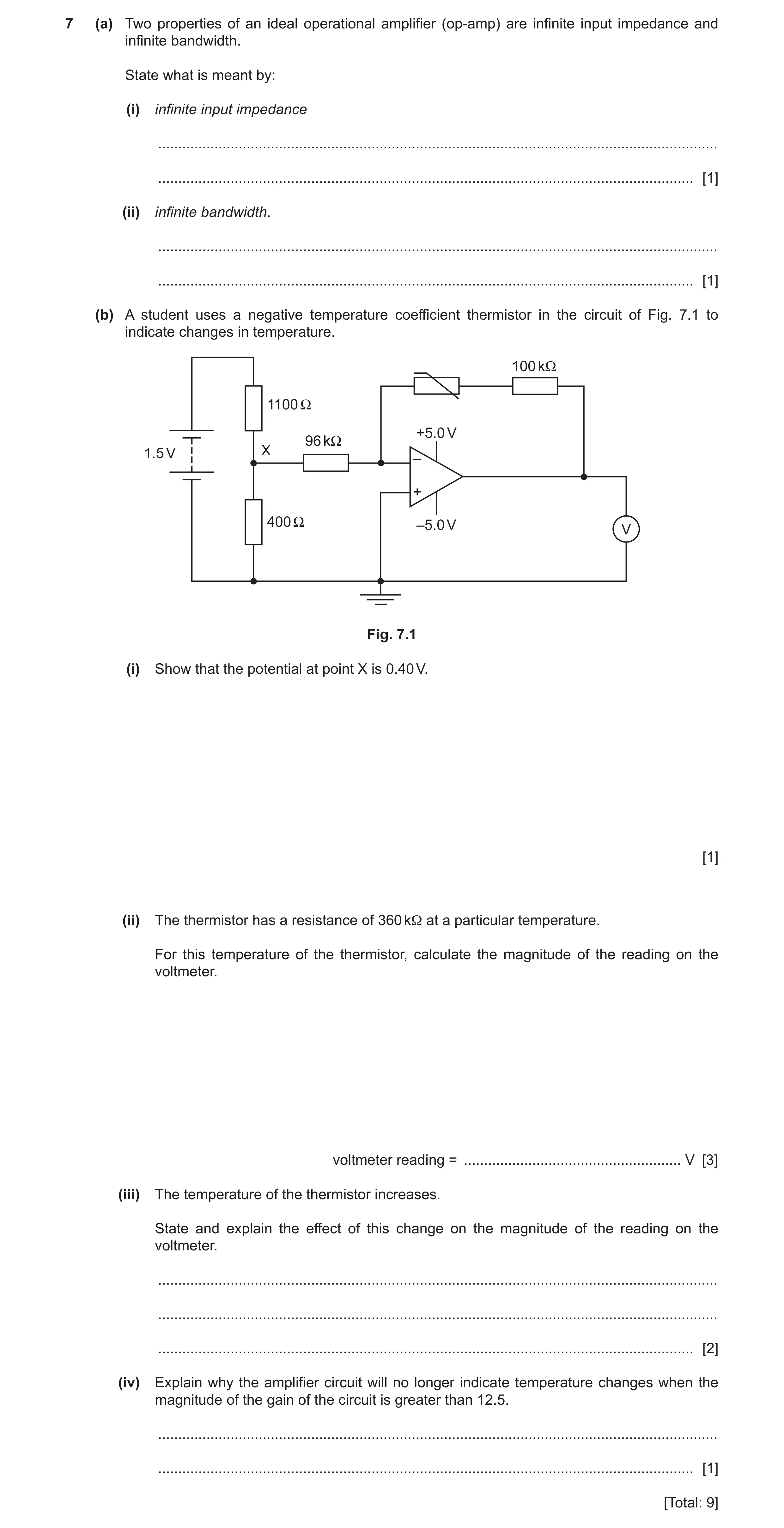
7 (a) Two properties of an ideal operational amplifier (op-amp) are infinite input impedance and infinite bandwidth. State what is meant by: (i) infinite input impedance … … [1] (ii) infinite bandwidth. … … [1] (b) A student uses a negative temperature coefficient thermistor in the circuit of Fig. 7.1 to indicate changes in temperature. 100 kΩ 1100 Ω +5.0 V 96 kΩ 1.5 V X – + 400 Ω –5.0 V V Fig. 7.1 (i) Show that the potential at point X is 0.40 V. [1] (ii) The thermistor has a resistance of 360 kΩ at a particular temperature. For this temperature of the thermistor, calculate the magnitude of the reading on the voltmeter. voltmeter reading = … V [3] (iii) The temperature of the thermistor increases. State and explain the effect of this change on the magnitude of the reading on the voltmeter. … … … [2] (iv) Explain why the amplifier circuit will no longer indicate temperature changes when the magnitude of the gain of the circuit is greater than 12.5. … … [1] [Total: 9]
9 marks
Mark scheme: 7(a)(i) no current enters/leaves the input B1 7(a)(ii) gain is the same for all frequencies B1 7(b)(i) VIN = 1.5 × 400 / (400 + 1100) = 0.40 V or VIN = 1.5 – (1.5 × 1100 / 1500) = 0.40 V or (1.5 – VIN) / 1100 = VIN / 400 so VIN = 0.40 V A1 7(b)(ii) gain = (–) Rf/Ri C1 VOUT/0.40 = (360 + 100) / 96 C1 VOUT = 1.9 V A1 7(b)(iii) resistance of thermistor decreases B1 (magnitude of) gain decreases so reading decreases B1 7(b)(iv) (at gain 12.5) VOUT is 5.0 V, so (above gain 12.5) output becomes saturated B1 Question Answer Marks
This question in 9702/42 May/June 2021
Q23 · State two properties of an ideal operational amplifier (op-amp) 9702/41 Oct/Nov 2021
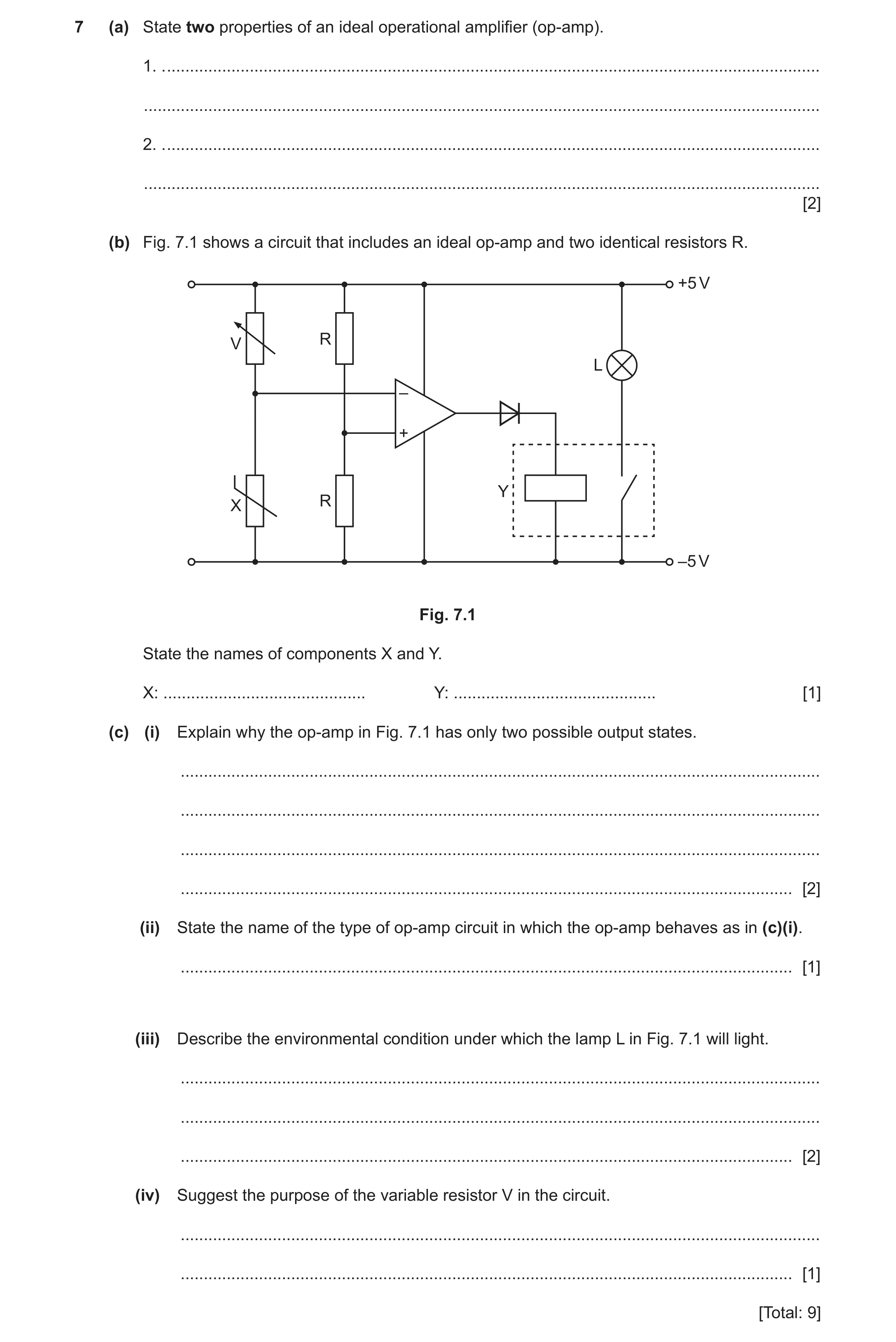
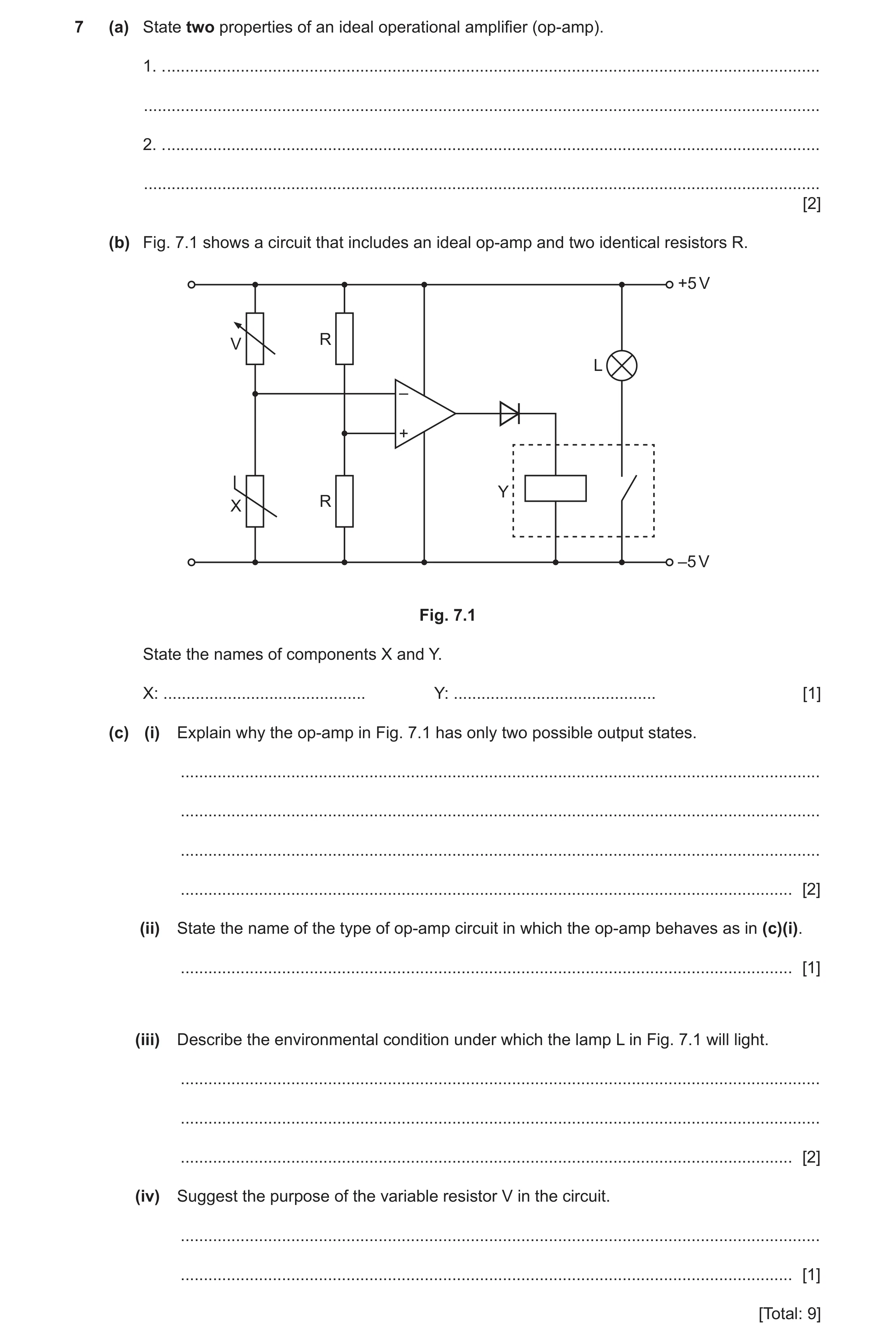
7 (a) State two properties of an ideal operational amplifier (op-amp). 1. . … … 2. . … … [2] (b) Fig. 7.1 shows a circuit that includes an ideal op-amp and two identical resistors R. +5 V R V L – + Y R X –5 V Fig. 7.1 State the names of components X and Y. X: … Y: … [1] (c) (i) Explain why the op-amp in Fig. 7.1 has only two possible output states. … … … … [2] (ii) State the name of the type of op-amp circuit in which the op-amp behaves as in (c)(i). … [1] (iii) Describe the environmental condition under which the lamp L in Fig. 7.1 will light. … … … [2] (iv) Suggest the purpose of the variable resistor V in the circuit. … … [1] [Total: 9]
9 marks
Mark scheme: 7(a) • infinite (open-loop) gain • infinite slew rate • infinite input impedance • zero output impedance • infinite bandwidth Any two points, 1 mark each B2 7(b) X: thermistor and Y: relay B1 7(c)(i) (any) difference in voltage at the inputs causes output to saturate (because gain is very large) B1 saturates positively if V+ > V– and saturates negatively if V+ < V– B1 7(c)(ii) comparator B1 7(c)(iii) temperature M1 above a particular value A1 7(c)(iv) to adjust the temperature (at which the lamp illuminates/extinguishes) B1
This question in 9702/41 Oct/Nov 2021
Q24 · An operational amplifier (op-amp) has two input terminals and one output terminal 9702/42 Oct/Nov 2021
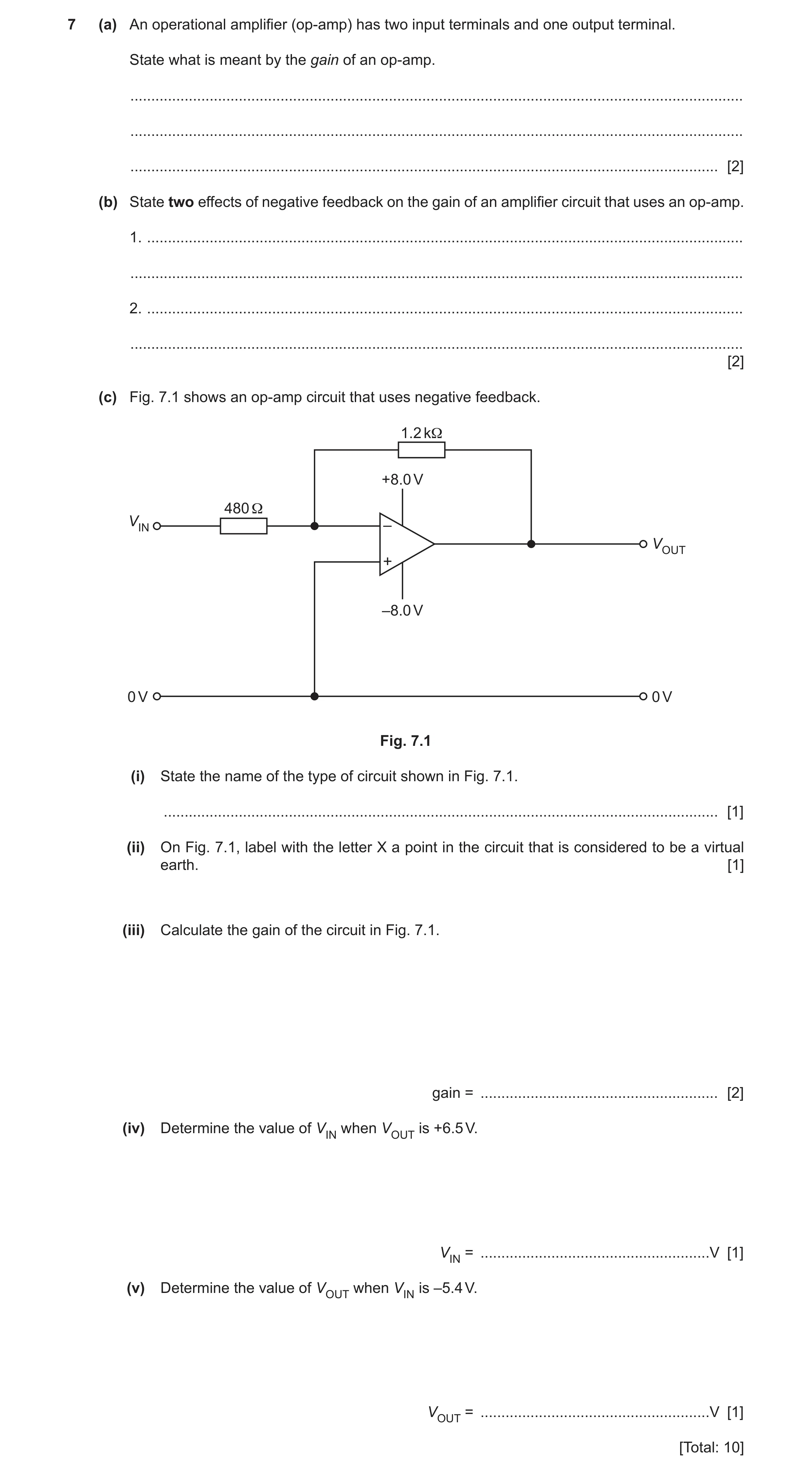
7 (a) An operational amplifier (op-amp) has two input terminals and one output terminal. State what is meant by the gain of an op-amp. … … … [2] (b) State two effects of negative feedback on the gain of an amplifier circuit that uses an op-amp. 1. … … 2. … … [2] (c) Fig. 7.1 shows an op-amp circuit that uses negative feedback. 1.2 kΩ +8.0 V 480 Ω VIN – VOUT + –8.0 V 0 V 0 V Fig. 7.1 (i) State the name of the type of circuit shown in Fig. 7.1. … [1] (ii) On Fig. 7.1, label with the letter X a point in the circuit that is considered to be a virtual earth. [1] (iii) Calculate the gain of the circuit in Fig. 7.1. gain = … [2] (iv) Determine the value of VIN when VOUT is +6.5 V. VIN = … V [1] (v) Determine the value of VOUT when VIN is –5.4 V. VOUT = … V [1] [Total: 10]
10 marks
Mark scheme: 7(a) output voltage / input voltage M1 input (voltage) is difference between (inverting and non-inverting) inputs A1 7(b) • reduces the gain • greater bandwidth • more stable Any two points, 1 mark each B2 7(c)(i) inverting amplifier B1 7(c)(ii) X marked anywhere between right-hand edge of 480 Ω resistor, left-hand edge of 1.2 kΩ resistor and the inverting input B1 7(c)(iii) gain = (–)Rf / Ri C1 = (–)1200 / 480 = –2.5 A1 7(c)(iv) VIN = 6.5 / (–2.5) = –2.6 V A1 7(c)(v) (–2.5) × (–5.4) = +13.5 V, and so output saturates VOUT = (+)8.0 V A1
This question in 9702/42 Oct/Nov 2021
Q25 · State two properties of an ideal operational amplifier (op-amp) 9702/43 Oct/Nov 2021
7 (a) State two properties of an ideal operational amplifier (op-amp). 1. . … … 2. . … … [2] (b) Fig. 7.1 shows a circuit that includes an ideal op-amp and two identical resistors R. +5 V R V L – + Y R X –5 V Fig. 7.1 State the names of components X and Y. X: … Y: … [1] (c) (i) Explain why the op-amp in Fig. 7.1 has only two possible output states. … … … … [2] (ii) State the name of the type of op-amp circuit in which the op-amp behaves as in (c)(i). … [1] (iii) Describe the environmental condition under which the lamp L in Fig. 7.1 will light. … … … [2] (iv) Suggest the purpose of the variable resistor V in the circuit. … … [1] [Total: 9]
9 marks
Mark scheme: 7(a) • infinite (open-loop) gain • infinite slew rate • infinite input impedance • zero output impedance • infinite bandwidth Any two points, 1 mark each B2 7(b) X: thermistor and Y: relay B1 7(c)(i) (any) difference in voltage at the inputs causes output to saturate (because gain is very large) B1 saturates positively if V+ > V– and saturates negatively if V+ < V– B1 7(c)(ii) comparator B1 7(c)(iii) temperature M1 above a particular value A1 7(c)(iv) to adjust the temperature (at which the lamp illuminates/extinguishes) B1
This question in 9702/43 Oct/Nov 2021
 12 / 36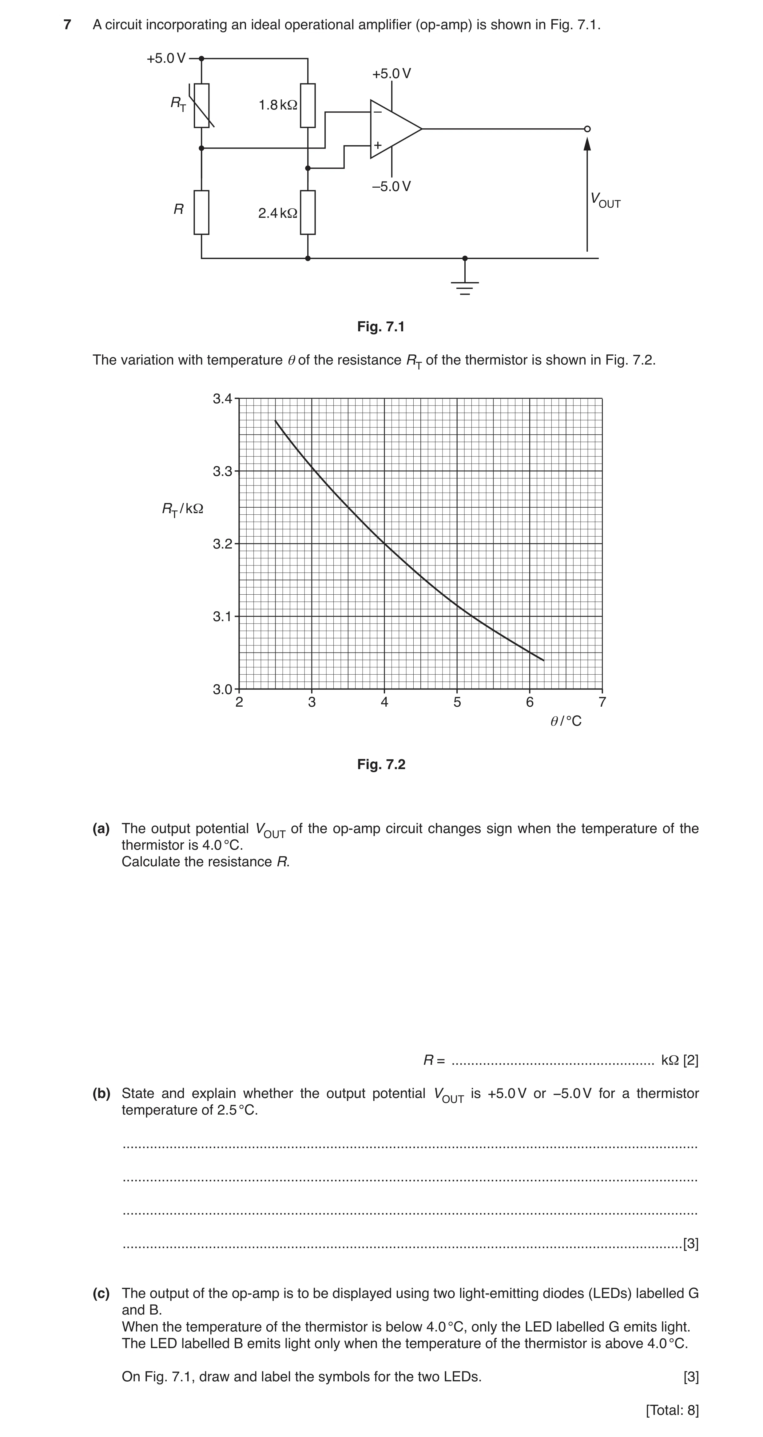
 15 / 36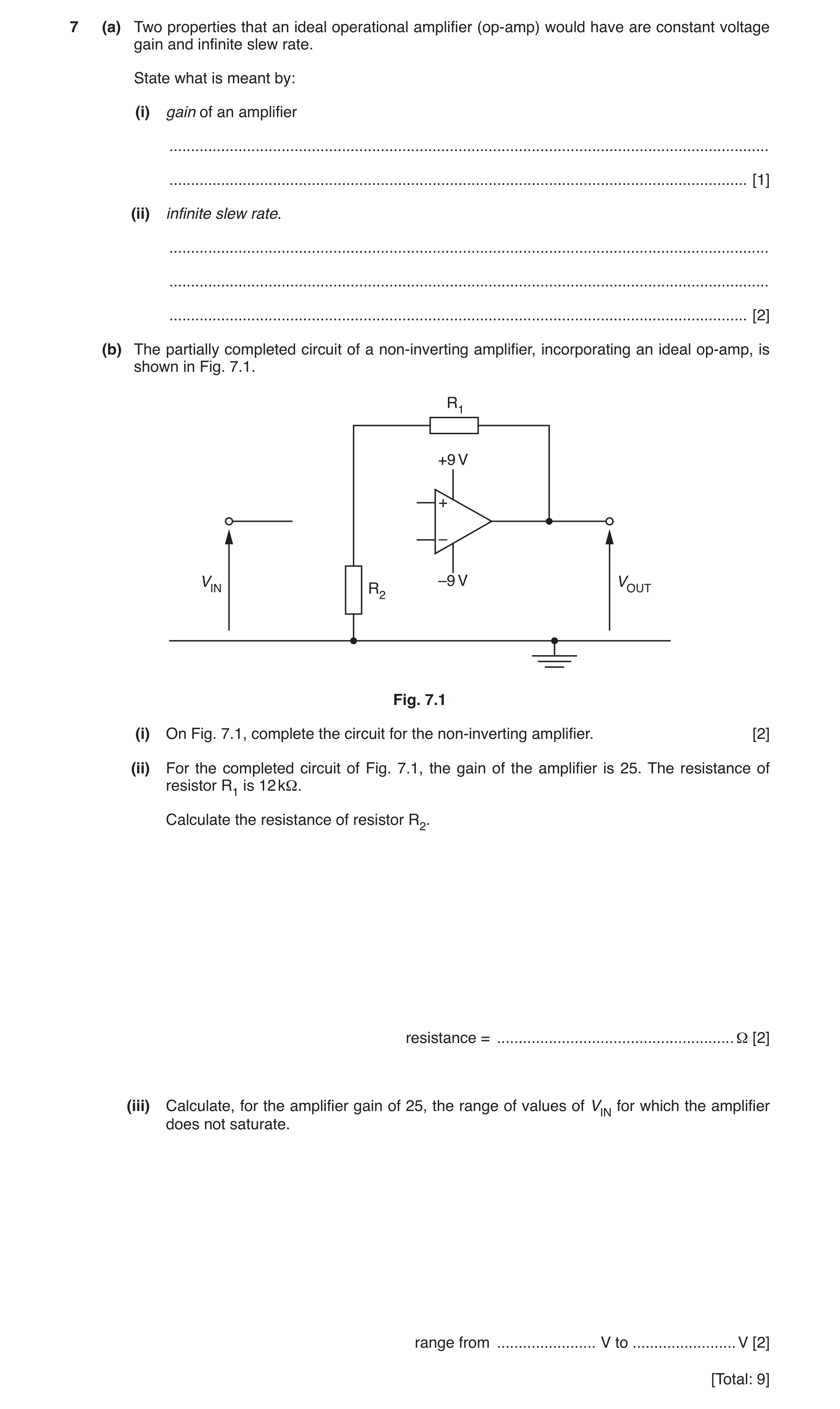
 19 / 36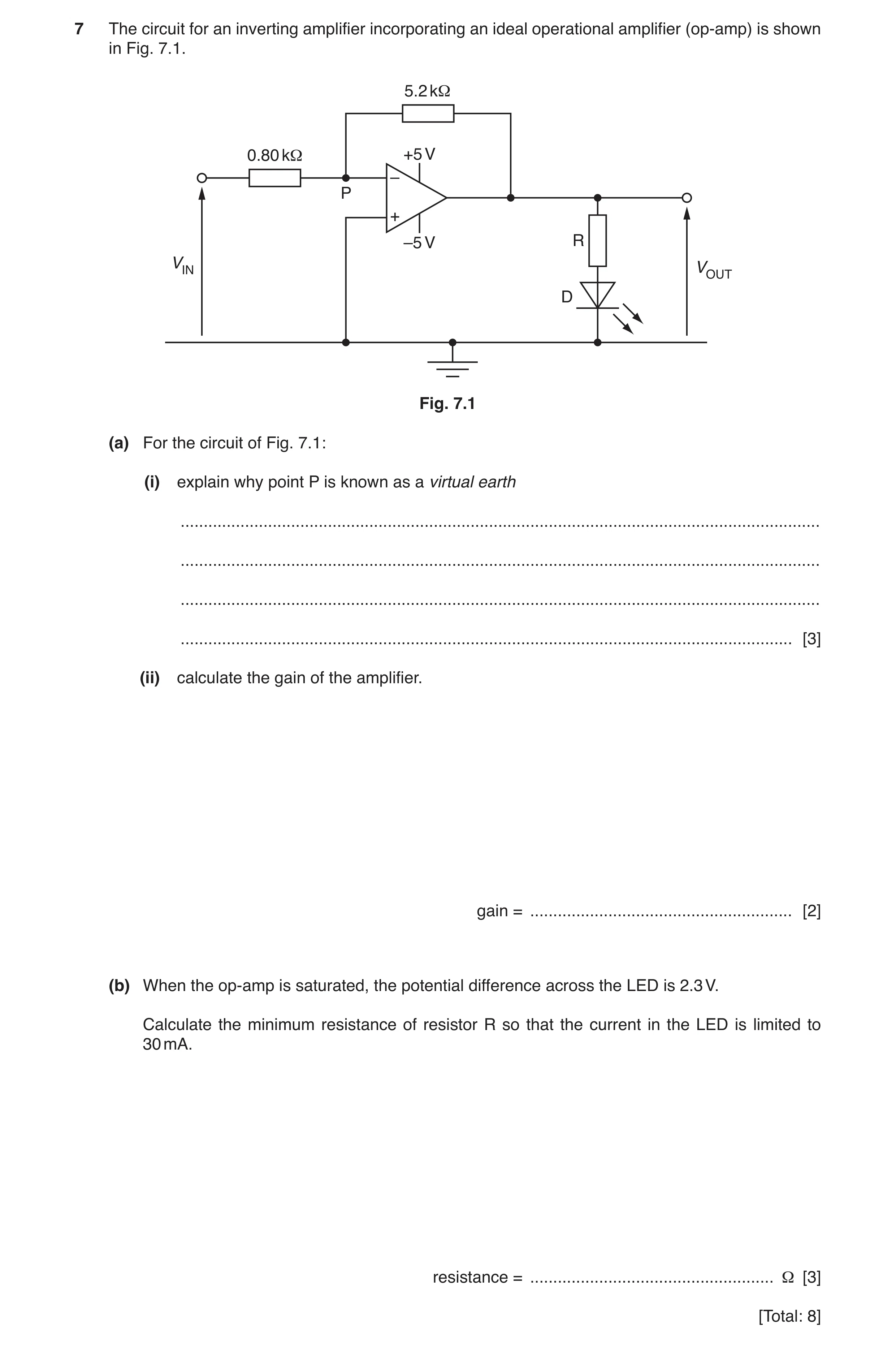
 10
10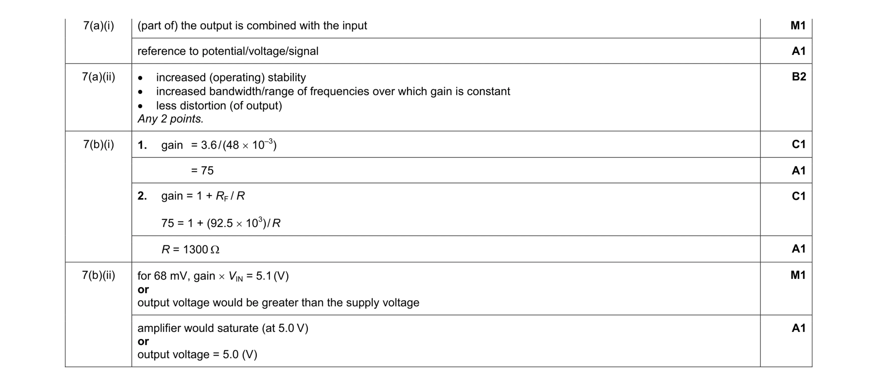 10
10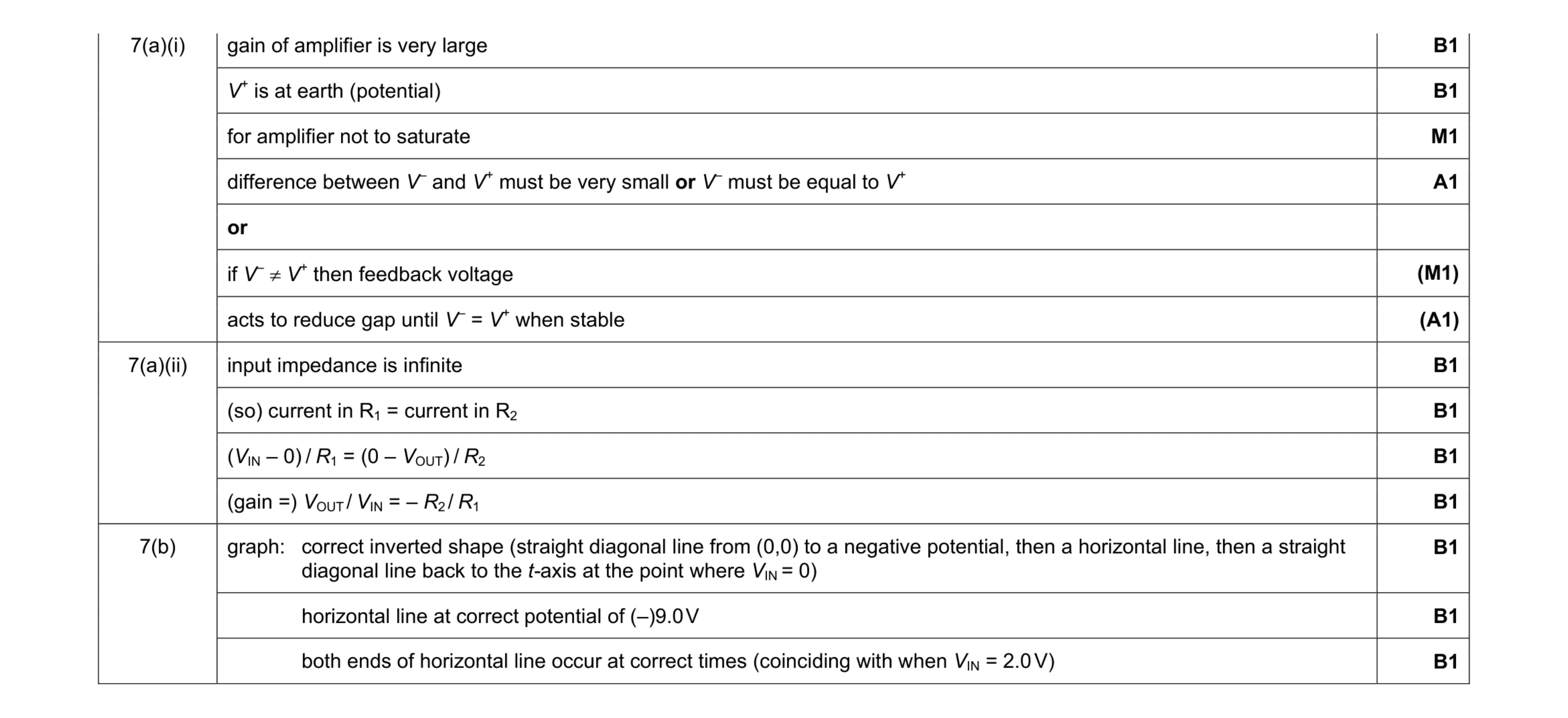 11
11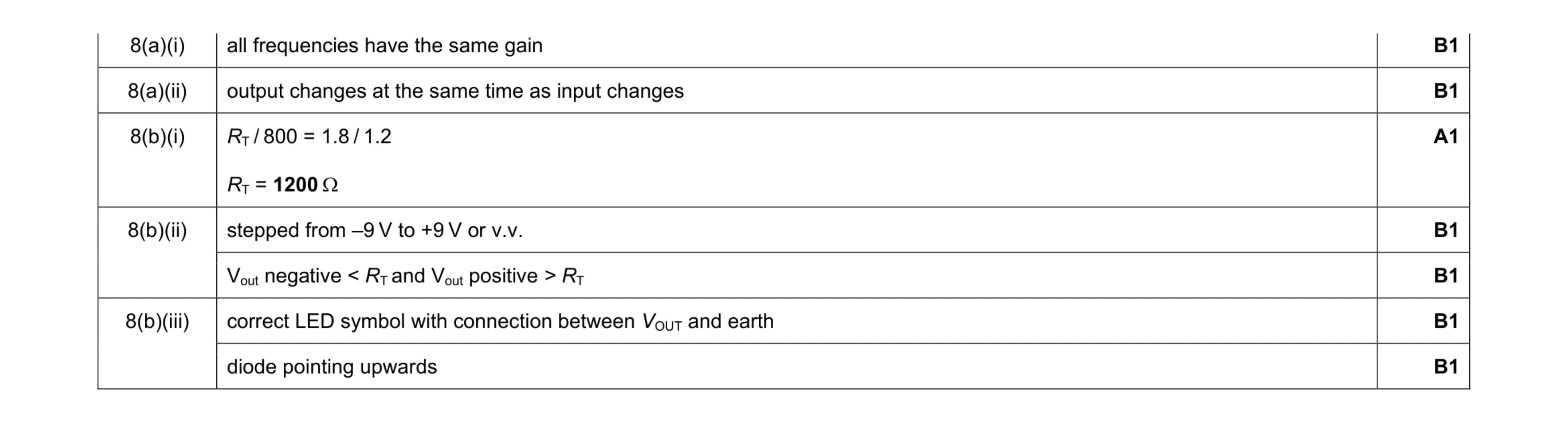 7
7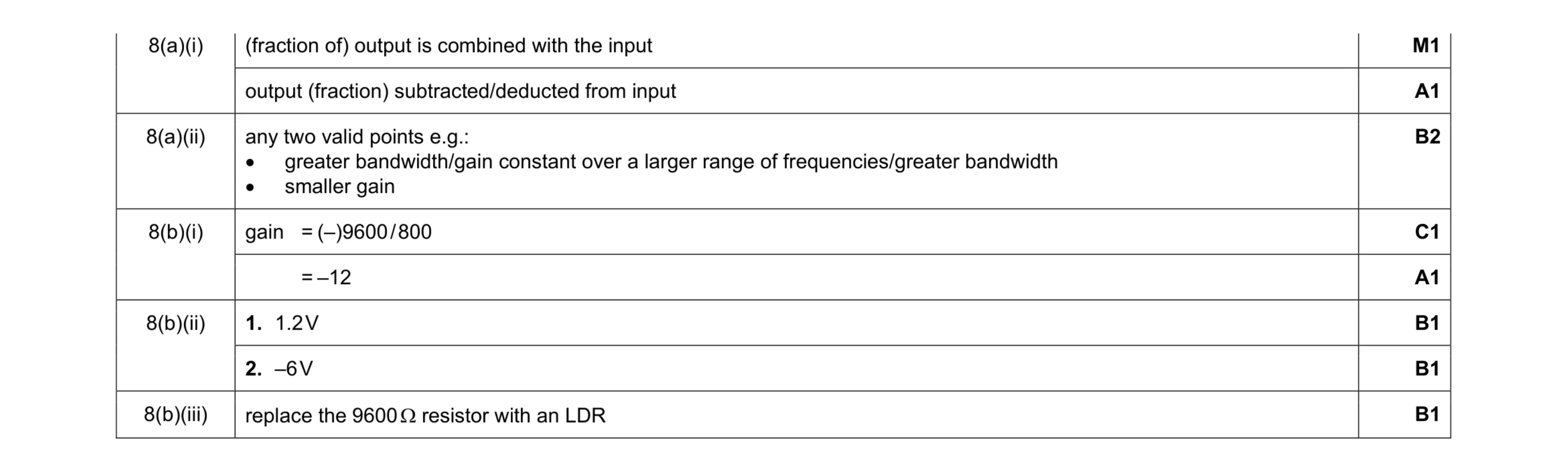 9
9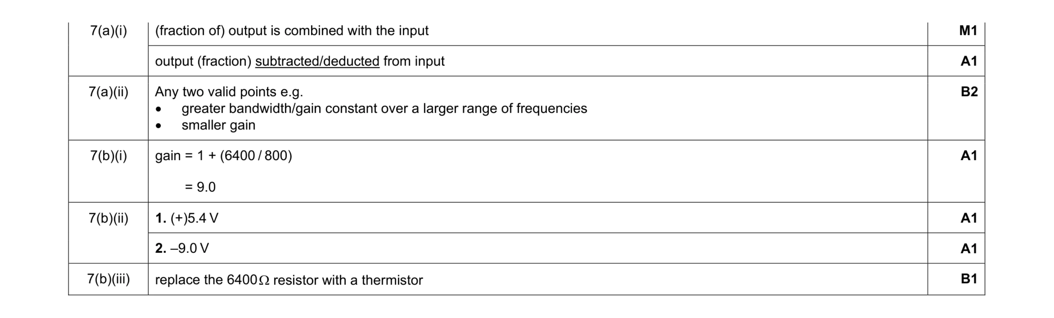 8
8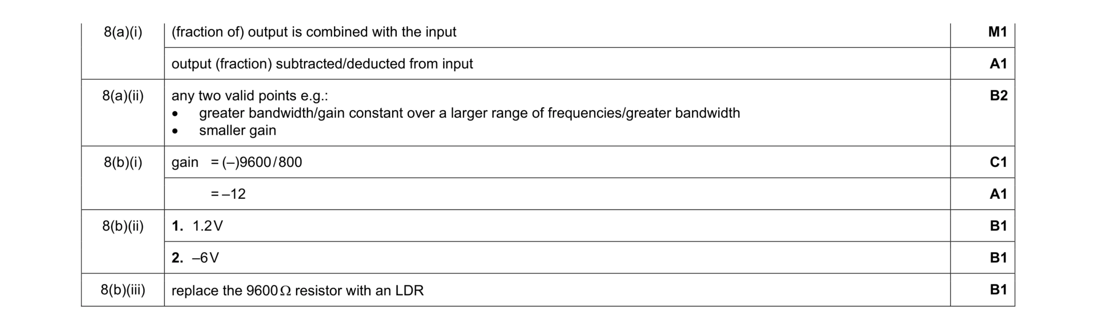 9
9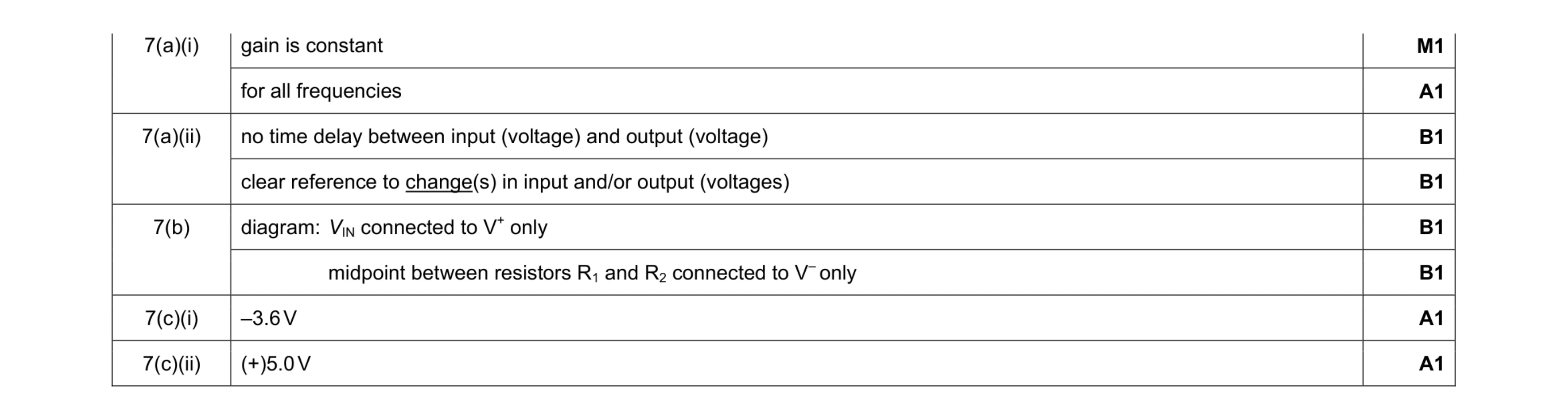 8
8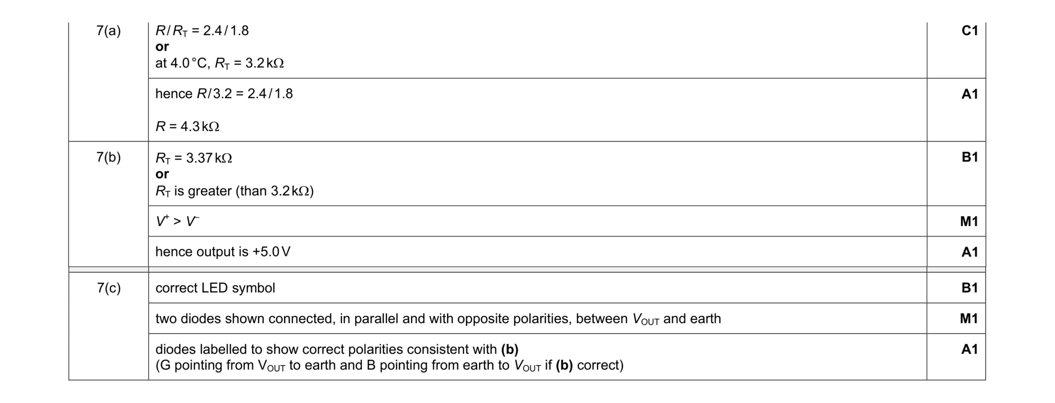 8
8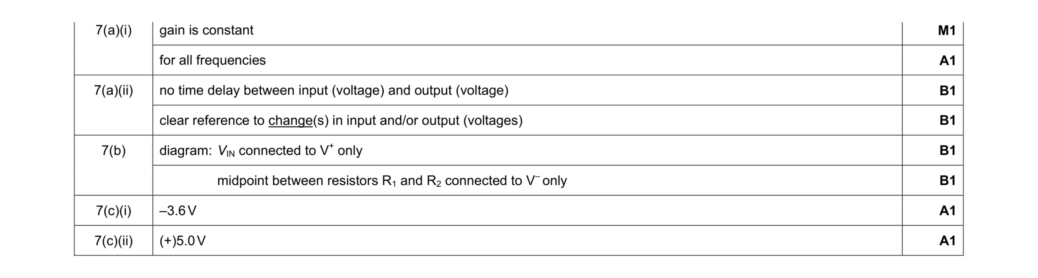 8
8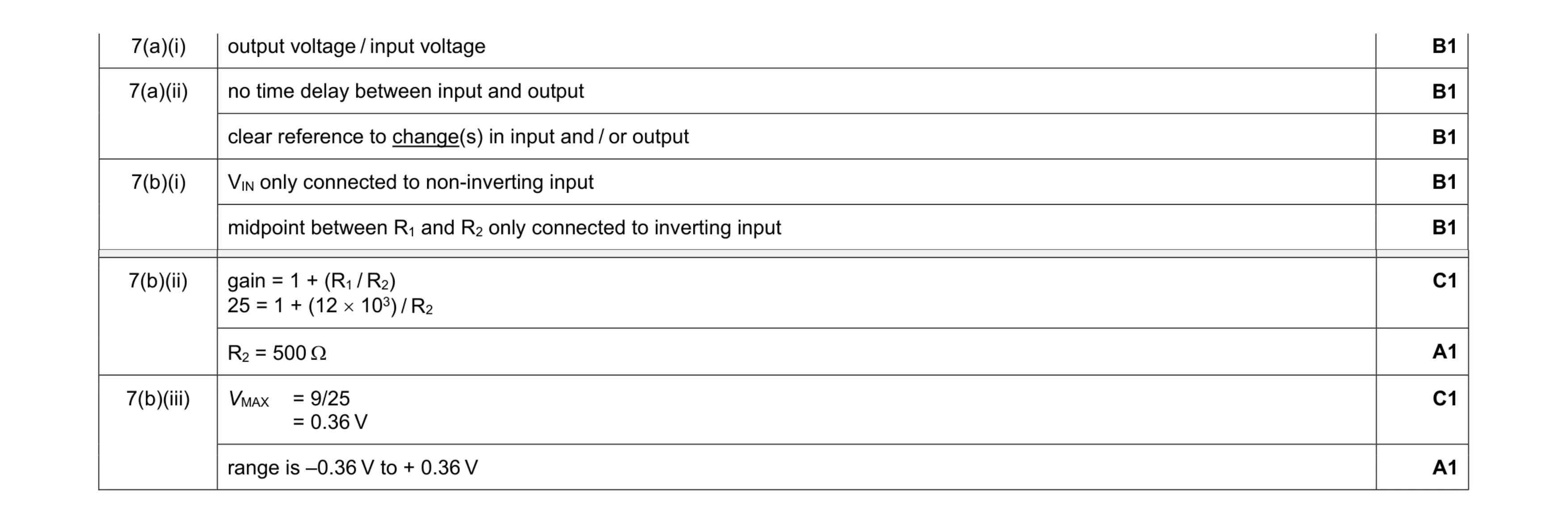 9
9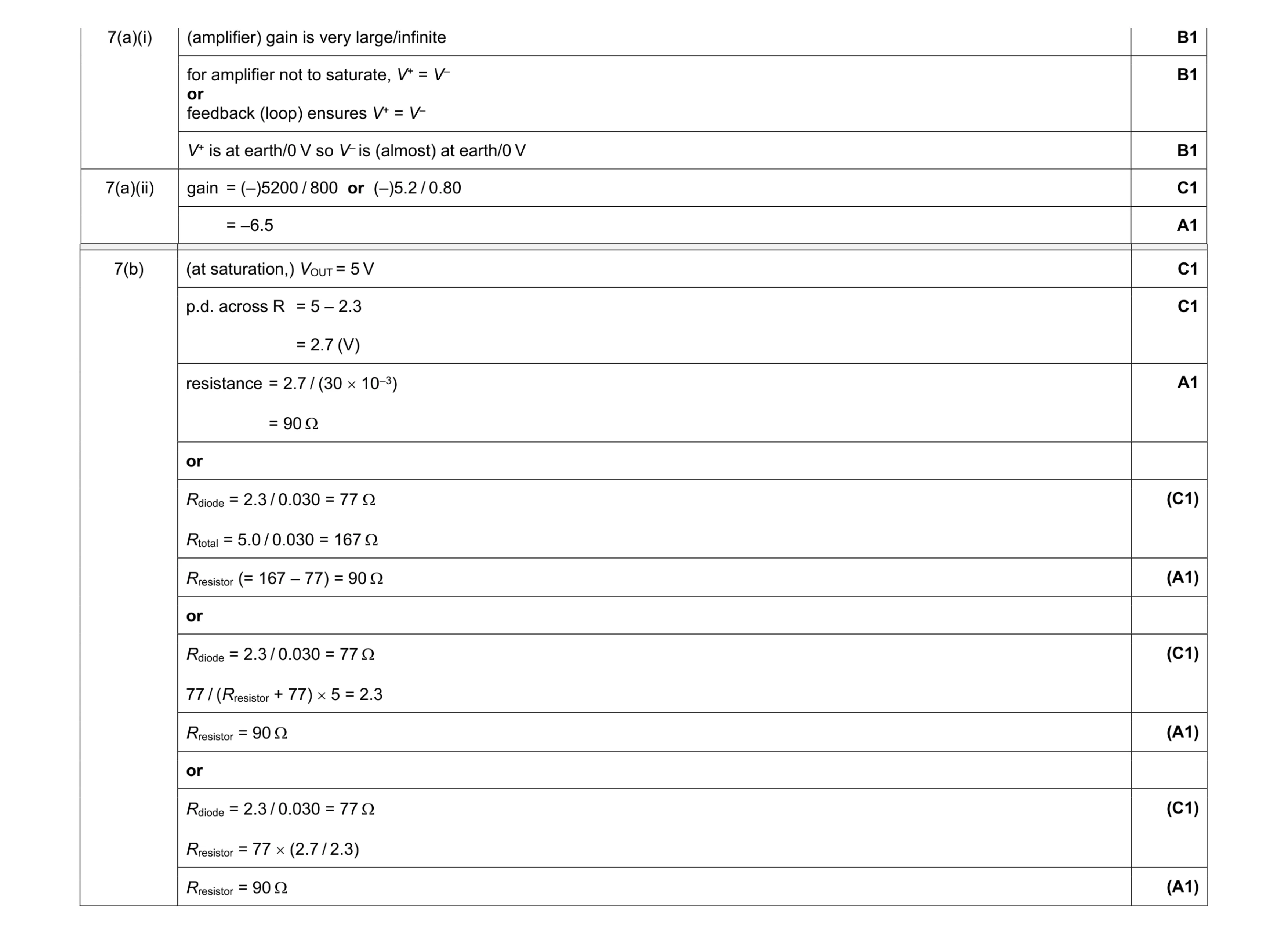 8
8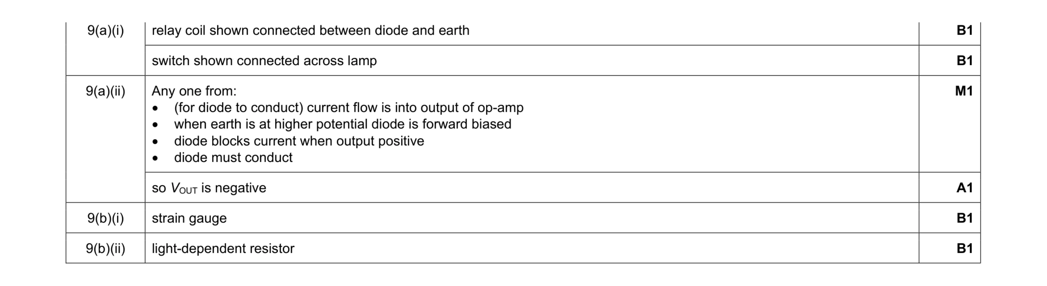 6
6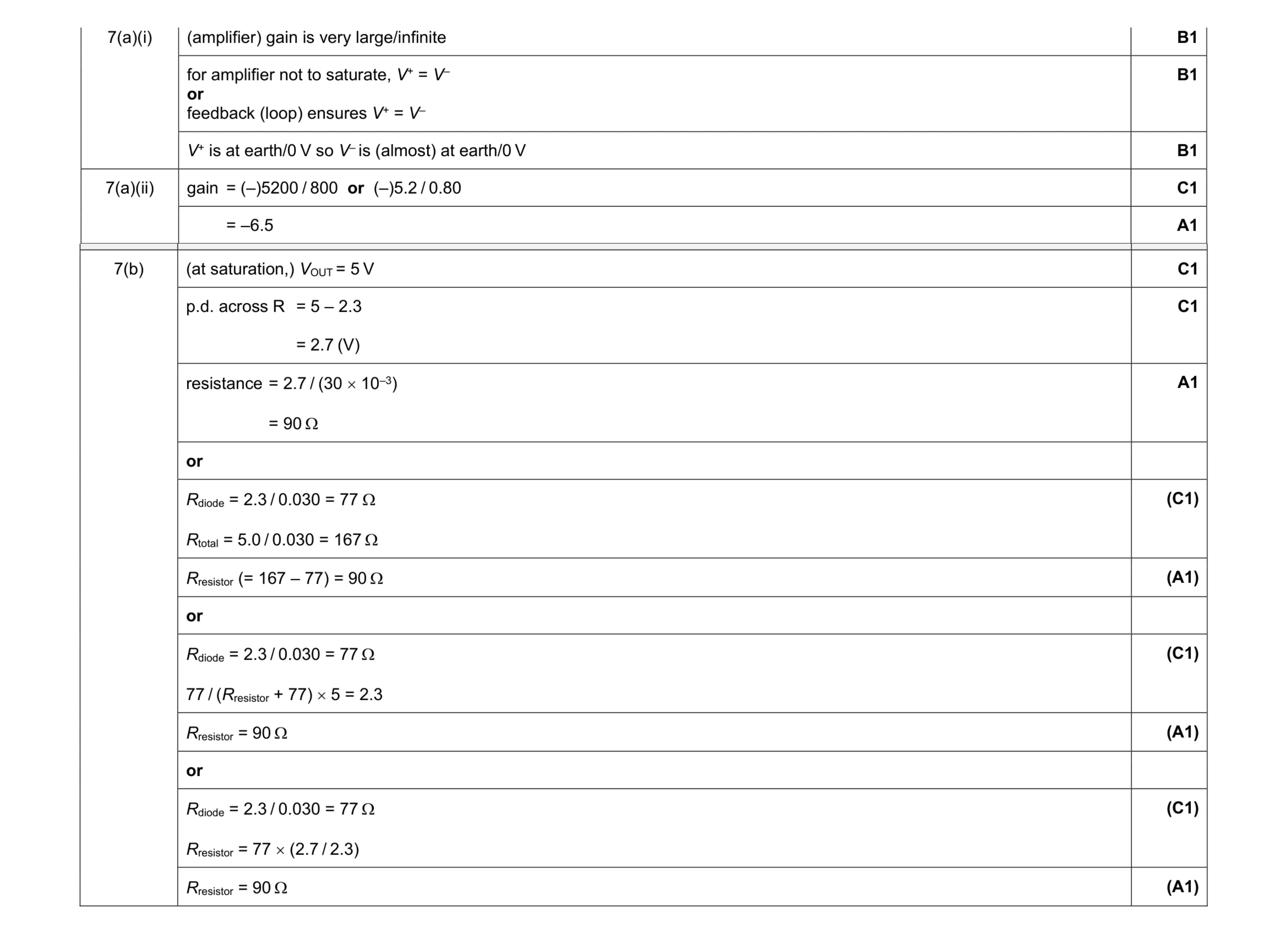 8
8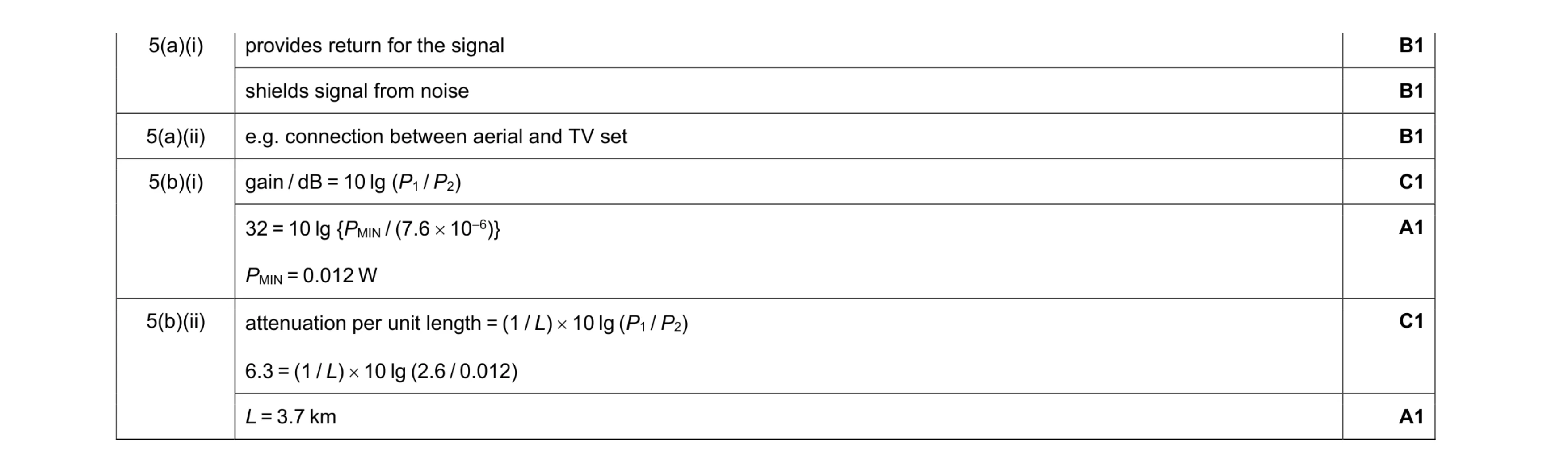 7
7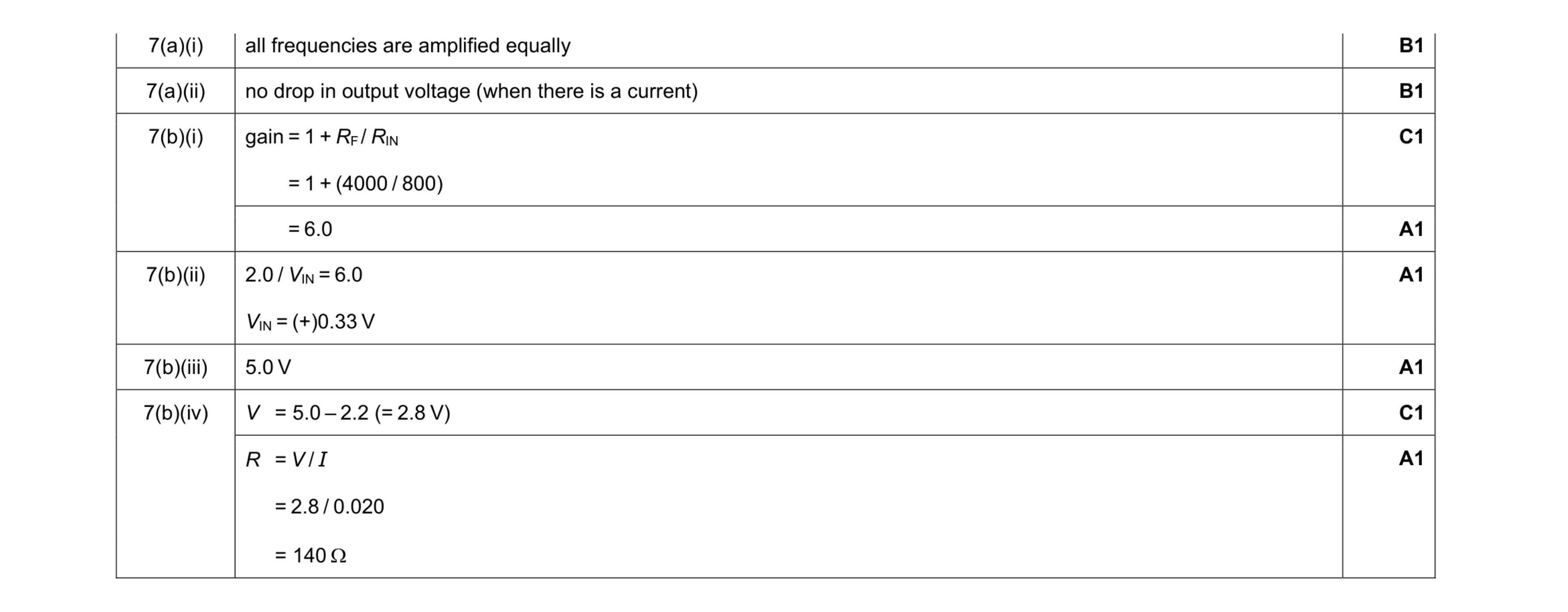 8
8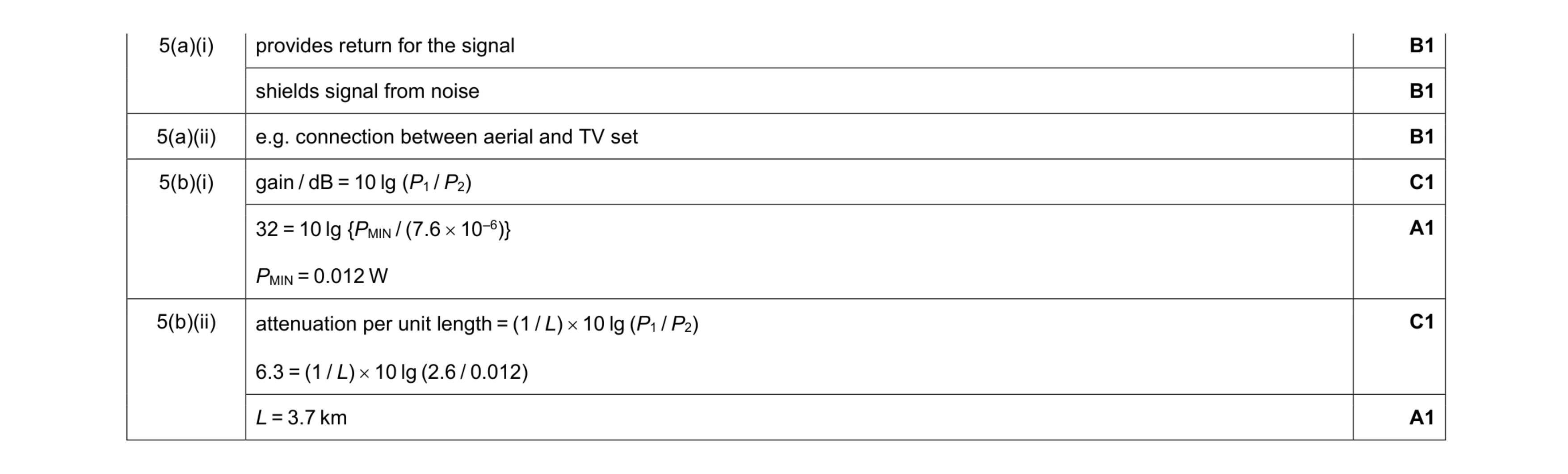 7
7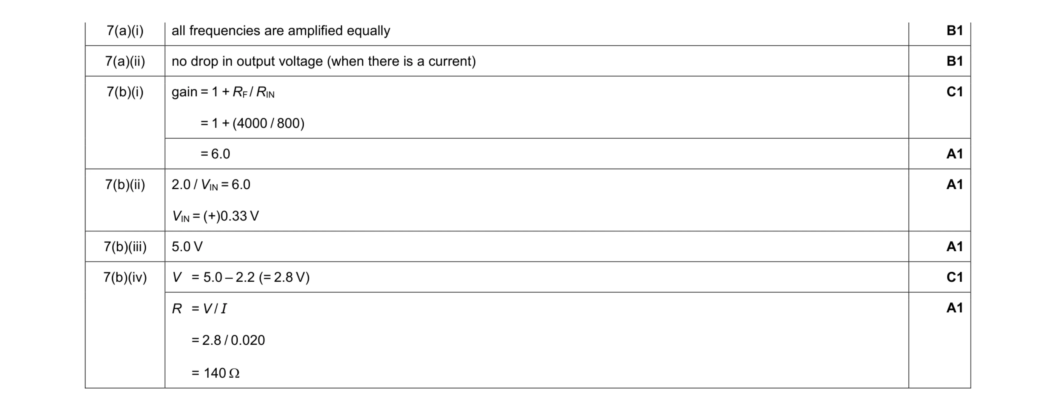 8
8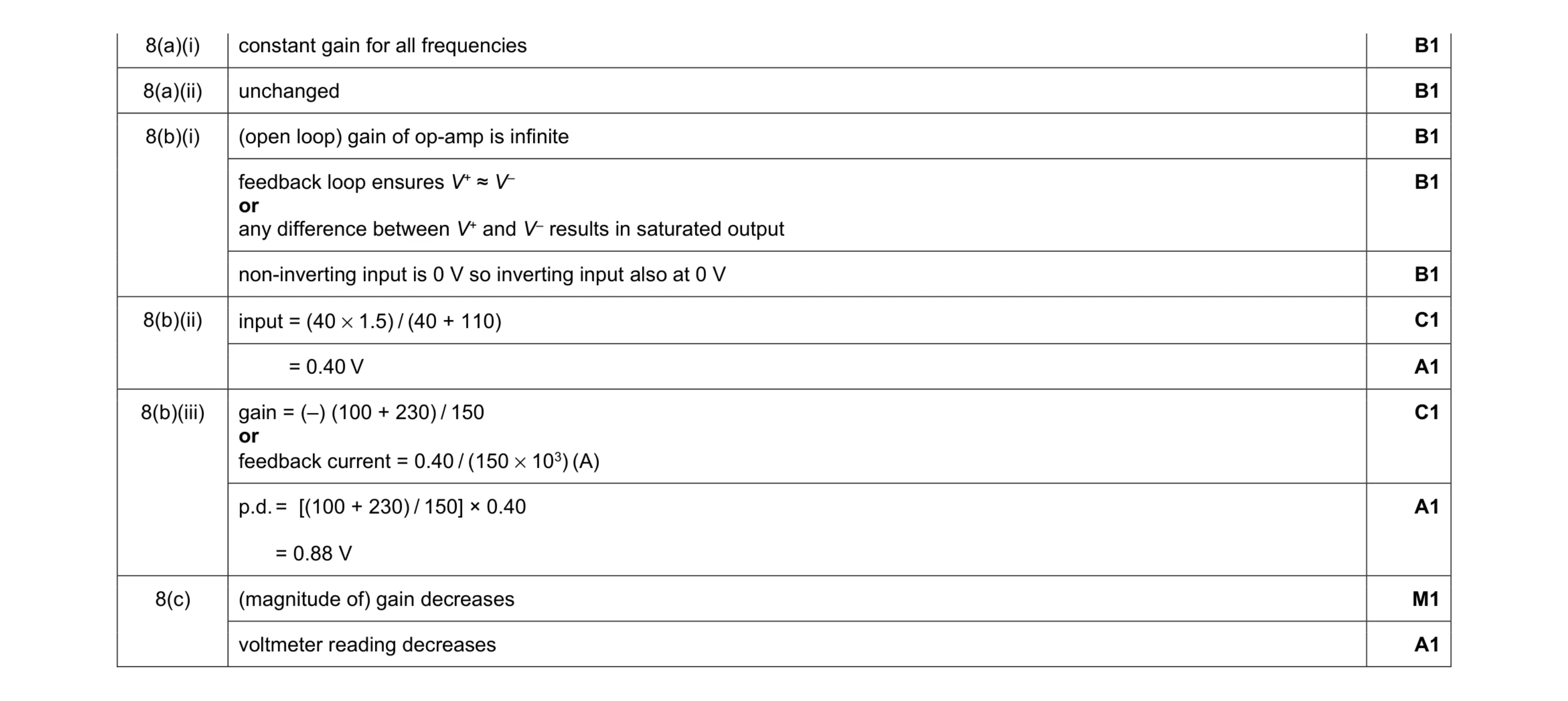 11
11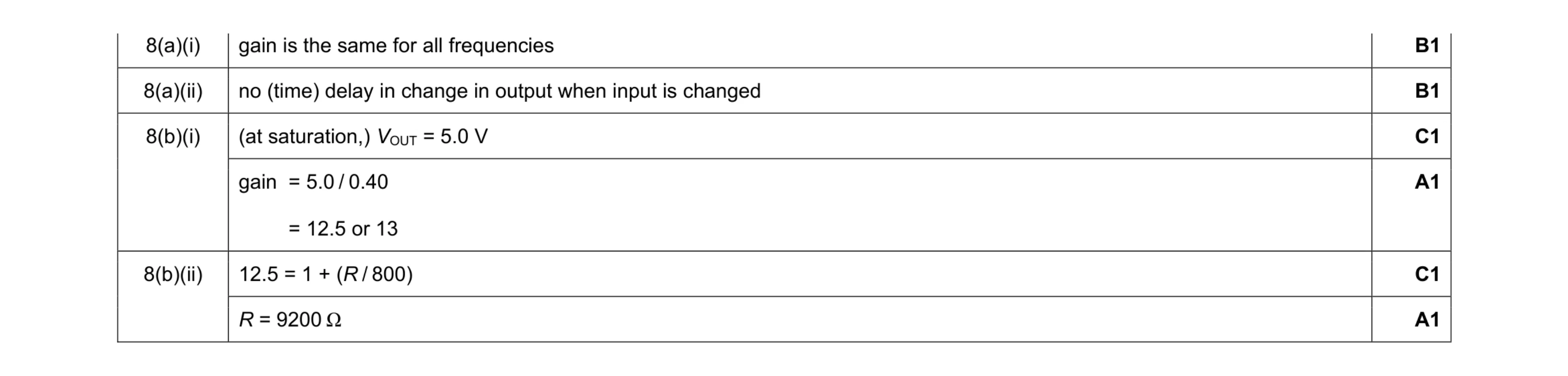 6
6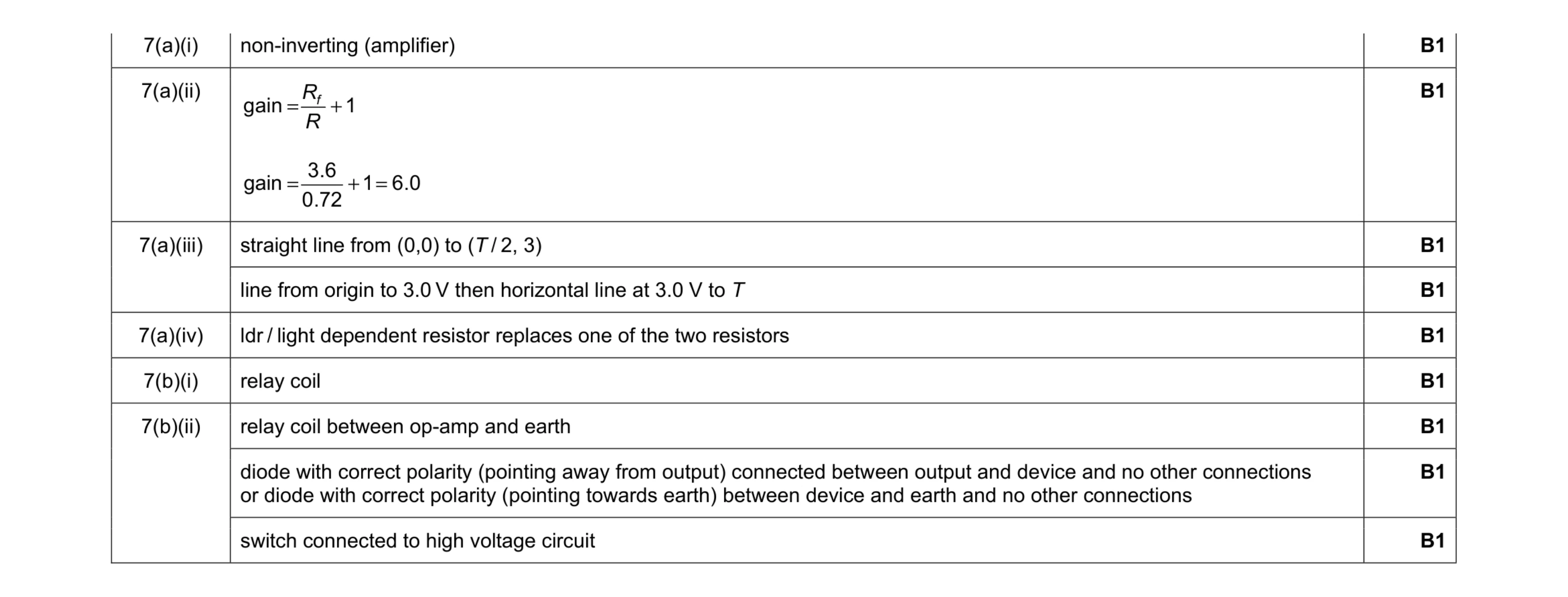 9
9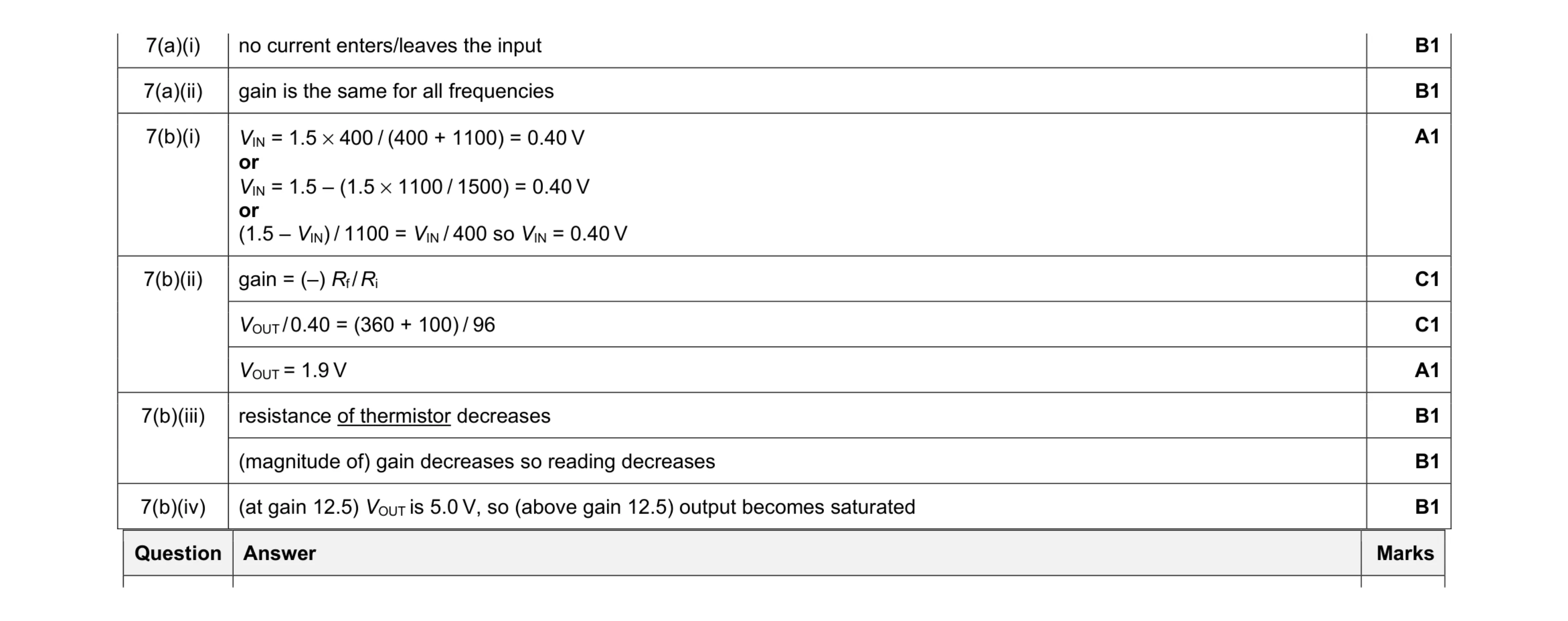 9
9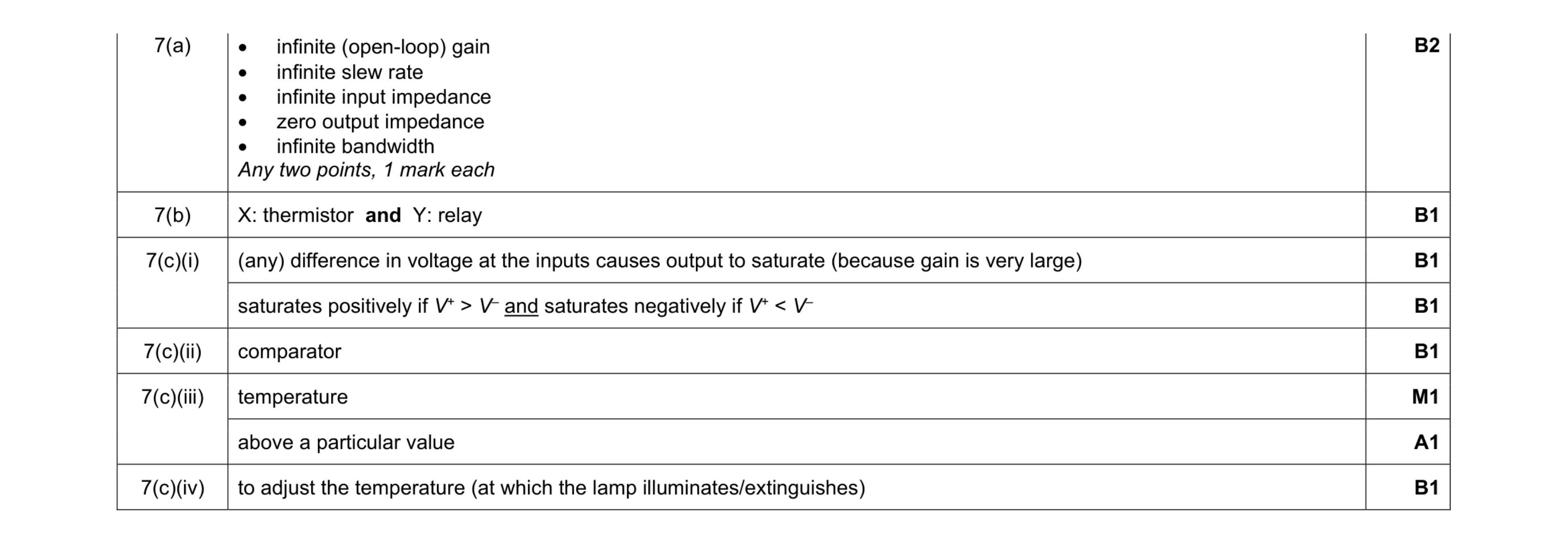 9
9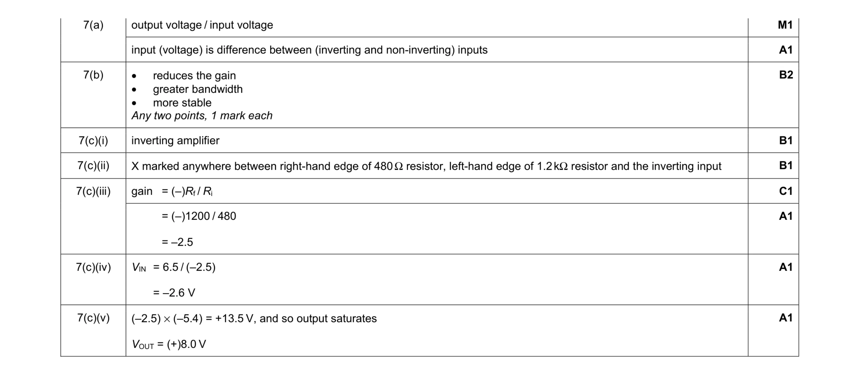 10
10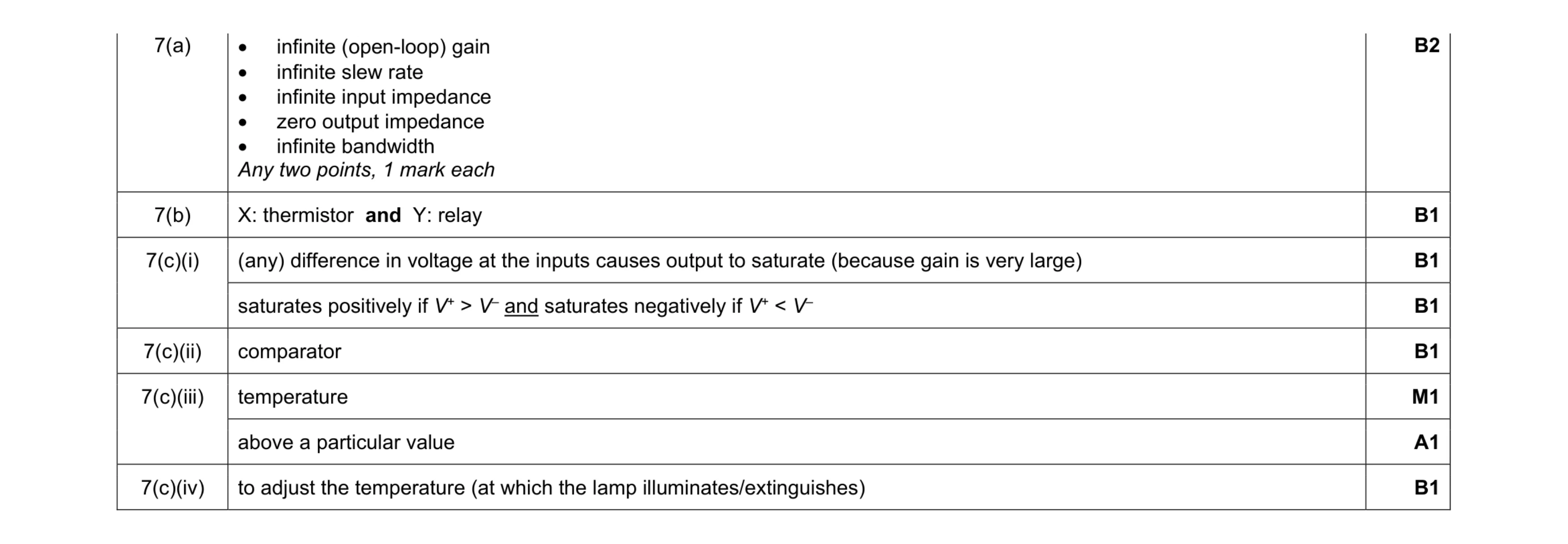 9
9