Questions as text
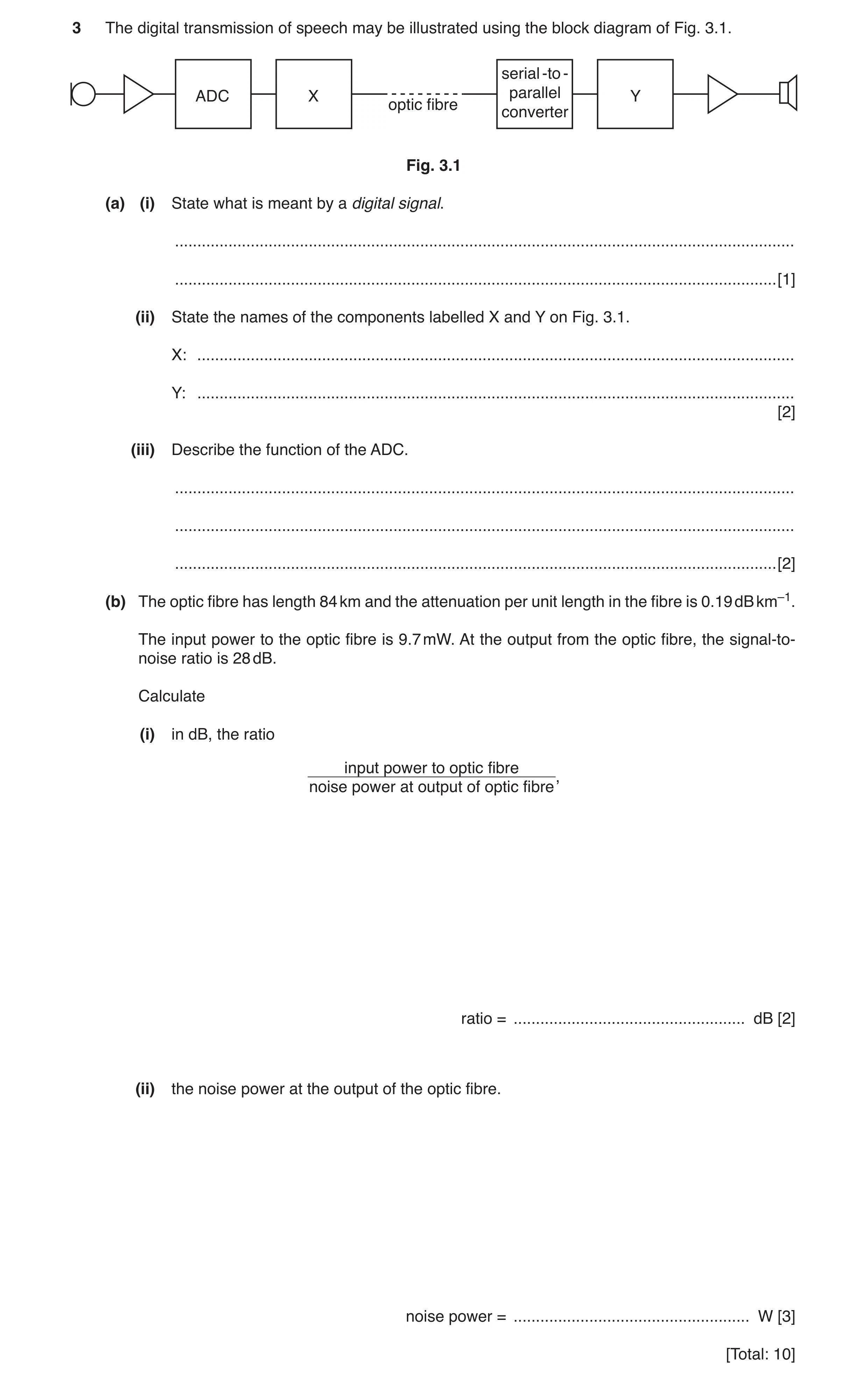
Q1 · The digital transmission of speech may be illustrated using the block diagram of Fig 9702/41 May/June 2017
3 The digital transmission of speech may be illustrated using the block diagram of Fig. 3.1. serial -to - ADC X parallel Y optic fibre converter Fig. 3.1 (a) (i) State what is meant by a digital signal. … … [1] (ii) State the names of the components labelled X and Y on Fig. 3.1. X: … Y: … [2] (iii) Describe the function of the ADC. … … … [2] (b) The optic fibre has length 84 km and the attenuation per unit length in the fibre is 0.19 dB km–1. The input power to the optic fibre is 9.7 mW. At the output from the optic fibre, the signal-to- noise ratio is 28 dB. Calculate (i) in dB, the ratio input power to optic fibre noise power at output of optic fibre, ratio = … dB [2] (ii) the noise power at the output of the optic fibre. noise power = … W [3] [Total: 10]
10 marks
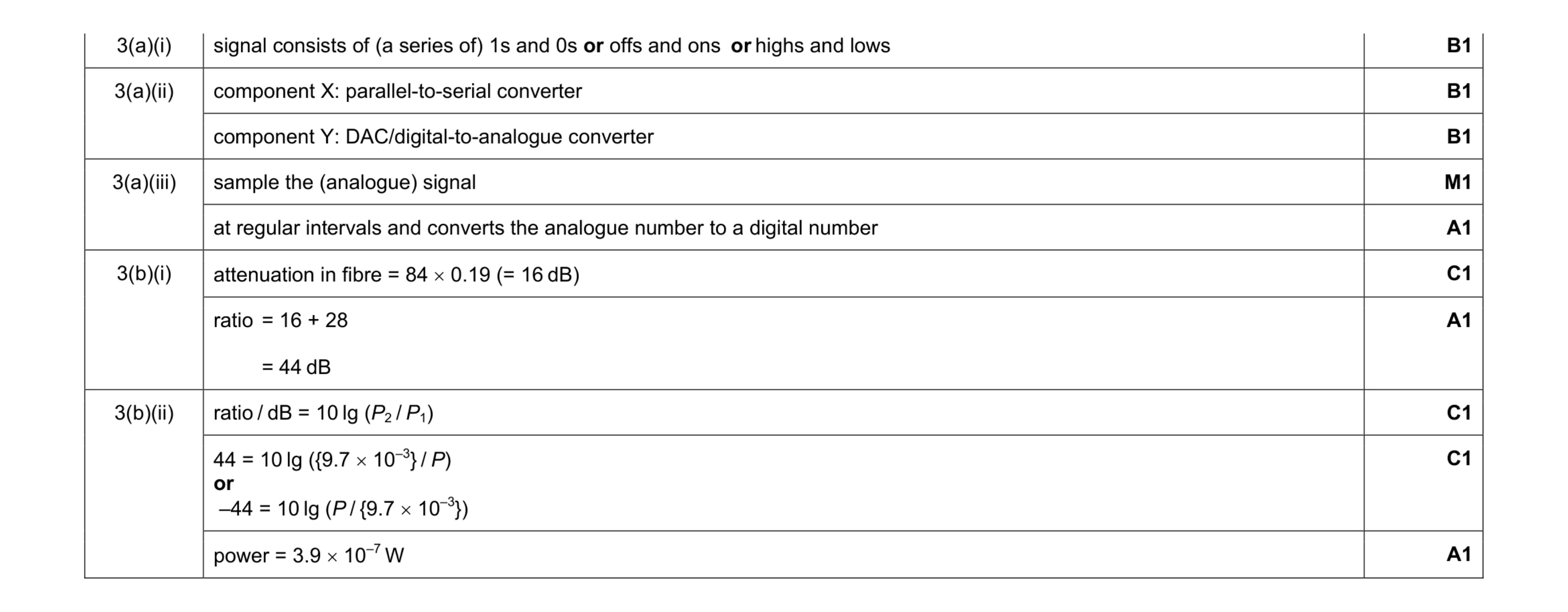
Mark scheme: 3(a)(i) signal consists of (a series of) 1s and 0s or offs and ons or highs and lows B1 3(a)(ii) component X: parallel-to-serial converter B1 component Y: DAC/digital-to-analogue converter B1 3(a)(iii) sample the (analogue) signal M1 at regular intervals and converts the analogue number to a digital number A1 3(b)(i) attenuation in fibre = 84 × 0.19 (= 16 dB) C1 ratio = 16 + 28 = 44 dB A1 3(b)(ii) ratio / dB = 10 lg (P2 / P1) C1 44 = 10 lg ({9.7 × 10⁻³} / P) or –44 = 10 lg (P / {9.7 × 10⁻³}) C1 power = 3.9 × 10⁻⁷ W A1
This question in 9702/41 May/June 2017
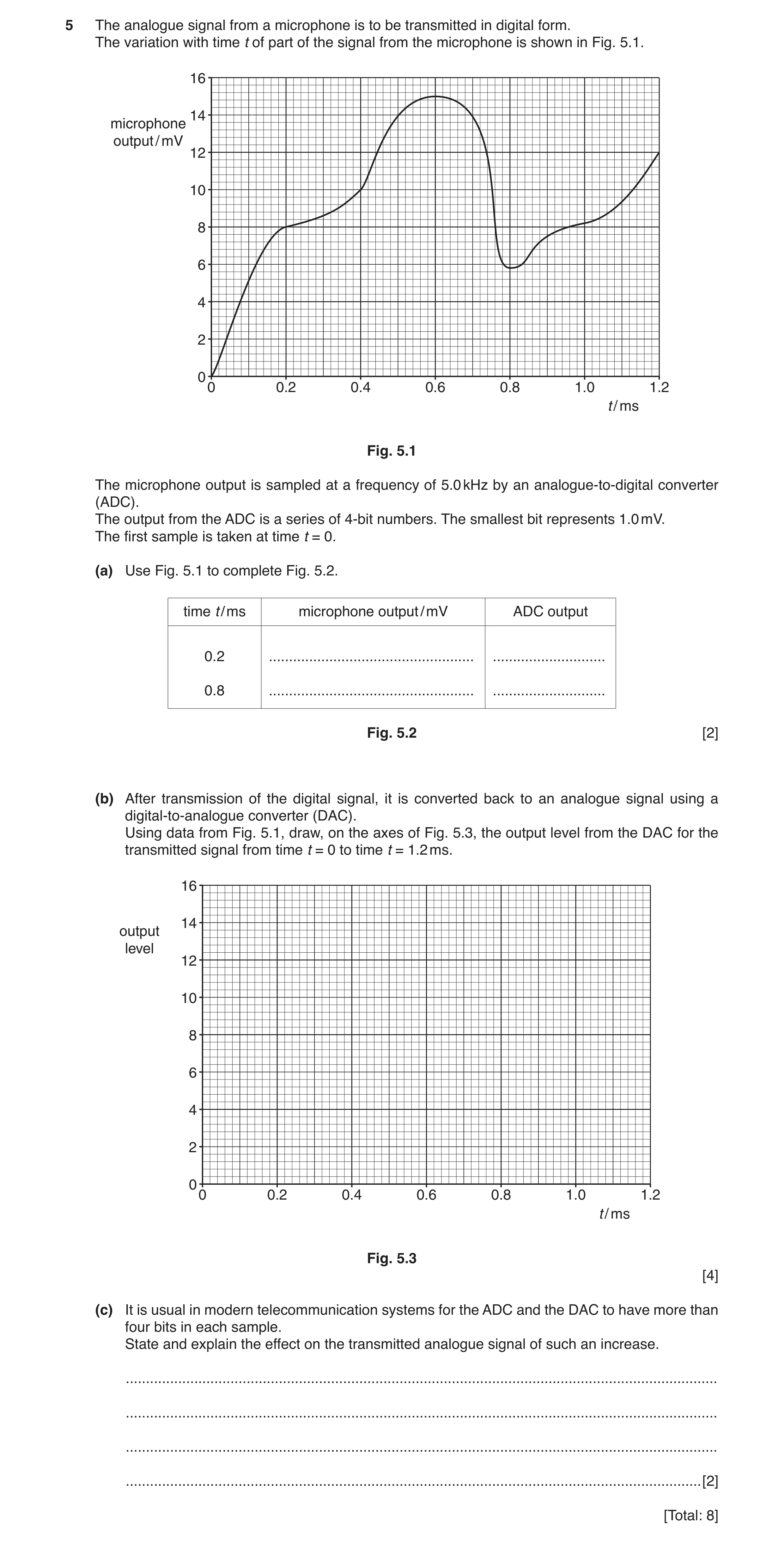
Q2 · The analogue signal from a microphone is to be transmitted in digital form 9702/42 Oct/Nov 2017
5 The analogue signal from a microphone is to be transmitted in digital form. The variation with time t of part of the signal from the microphone is shown in Fig. 5.1. 16 14 microphone output / mV 12 10 8 6 4 2 0 0 0.2 0.4 0.6 0.8 1.0 1.2 t / ms Fig. 5.1 The microphone output is sampled at a frequency of 5.0 kHz by an analogue-to-digital converter (ADC). The output from the ADC is a series of 4-bit numbers. The smallest bit represents 1.0 mV. The first sample is taken at time t = 0. (a) Use Fig. 5.1 to complete Fig. 5.2. time t / ms microphone output / mV ADC output 0.2 … … 0.8 … … Fig. 5.2 [2] (b) After transmission of the digital signal, it is converted back to an analogue signal using a digital-to-analogue converter (DAC). Using data from Fig. 5.1, draw, on the axes of Fig. 5.3, the output level from the DAC for the transmitted signal from time t = 0 to time t = 1.2 ms. 16 14 output level 12 10 8 6 4 2 0 0 0.2 0.4 0.6 0.8 1.0 1.2 t / ms Fig. 5.3 [4] (c) It is usual in modern telecommunication systems for the ADC and the DAC to have more than four bits in each sample. State and explain the effect on the transmitted analogue signal of such an increase. … … … … [2] [Total: 8]
8 marks
Mark scheme: 5(a) (0.2 ms) 8.0 (mV) 1000 B1 (0.8 ms) 5.8 (mV) 0101 B1 5(b) series of steps B1 all (step) changes are at 0.2 ms intervals B1 steps with correct levels at correct times (1 mark if five levels correct; 2 marks if all levels correct) level 0 8 10 15 5 8 time / ms 0–0.2 0.2–0.4 0.4–0.6 0.6–0.8 0.8–1.0 1.0–1.2 B2 5(c) smaller step heights (possible) B1 smaller changes (in input signal) can be seen/reproduced/represented or (allows) more accurate reproduction (of the input signal) B1
This question in 9702/42 Oct/Nov 2017
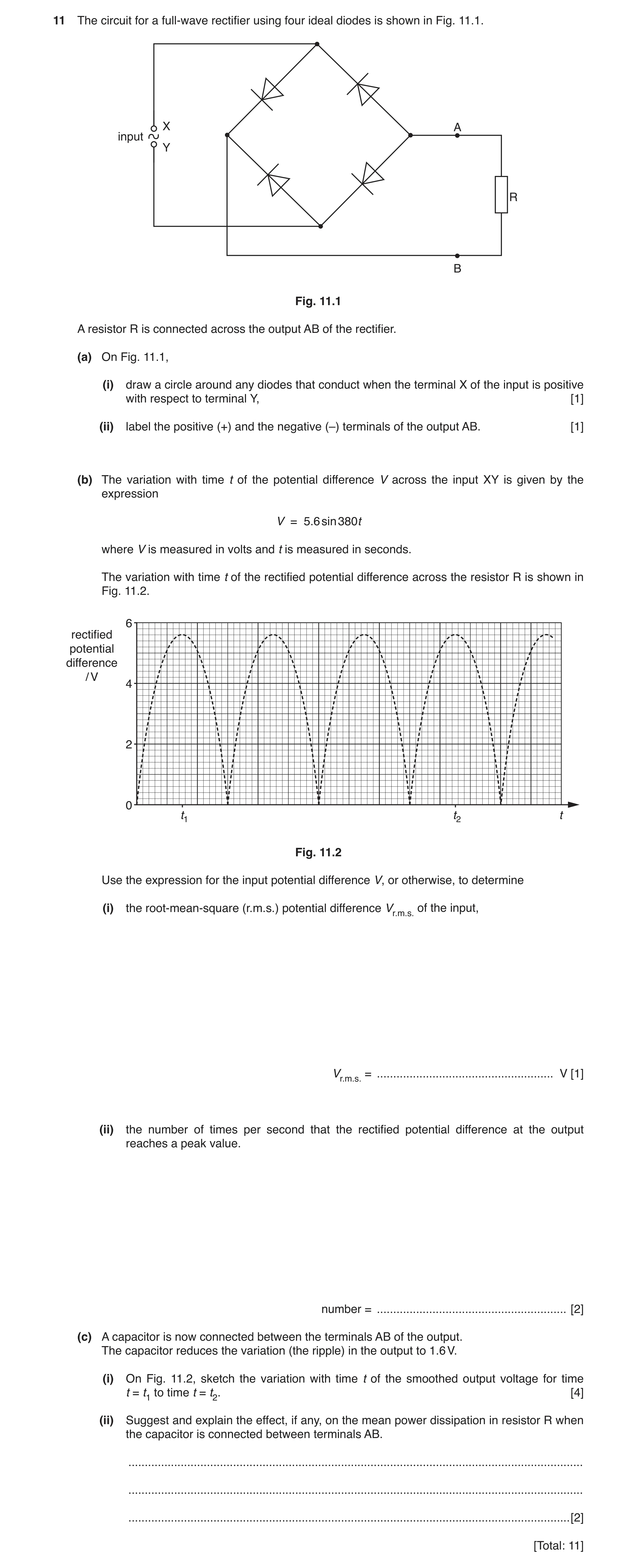
Q3 · The circuit for a full-wave rectifier using four ideal diodes is shown in Fig 9702/42 Oct/Nov 2017
11 The circuit for a full-wave rectifier using four ideal diodes is shown in Fig. 11.1. X A input Y R B Fig. 11.1 A resistor R is connected across the output AB of the rectifier. (a) On Fig. 11.1, (i) draw a circle around any diodes that conduct when the terminal X of the input is positive with respect to terminal Y, [1] (ii) label the positive (+) and the negative (–) terminals of the output AB. [1] (b) The variation with time t of the potential difference V across the input XY is given by the expression V = 5.6 sin 380t where V is measured in volts and t is measured in seconds. The variation with time t of the rectified potential difference across the resistor R is shown in Fig. 11.2. 6 rectified potential difference / V 4 2 0 t1 t2 t Fig. 11.2 Use the expression for the input potential difference V, or otherwise, to determine (i) the root-mean-square (r.m.s.) potential difference Vr.m.s. of the input, Vr.m.s. = … V [1] (ii) the number of times per second that the rectified potential difference at the output reaches a peak value. number = … [2] (c) A capacitor is now connected between the terminals AB of the output. The capacitor reduces the variation (the ripple) in the output to 1.6 V. (i) On Fig. 11.2, sketch the variation with time t of the smoothed output voltage for time t = t1 to time t = t2. [4] (ii) Suggest and explain the effect, if any, on the mean power dissipation in resistor R when the capacitor is connected between terminals AB. … … … [2] [Total: 11]
11 marks
Mark scheme: 11(a)(i) circles drawn only around the top left and bottom right diodes B1 11(a)(ii) B shown as (+)ve and A shown as (–)ve B1 11(b)(i) Vr.m.s. (= 5.6 / √2) = 4.0 V A1 11(b)(ii) 380 = 2πf or f = 60.5 Hz C1 number (= 2f ) = 120 A1 11(c)(i) peak values (all) unchanged B1 (all) minima shown at 4.0 V B1 three lines from near peak showing concave curves after leaving dotted line not ‘kinked’ and not cutting the peak reaching candidate’s minimum at the point where the decay meets the next dotted line B1 three lines drawn along the dotted lines showing rise in voltage from minima back to peak values B1 11(c)(ii) mean p.d. is higher or r.m.s. p.d. is higher or capacitor supplies energy to resistor M1 so (mean) power increases A1
This question in 9702/42 Oct/Nov 2017
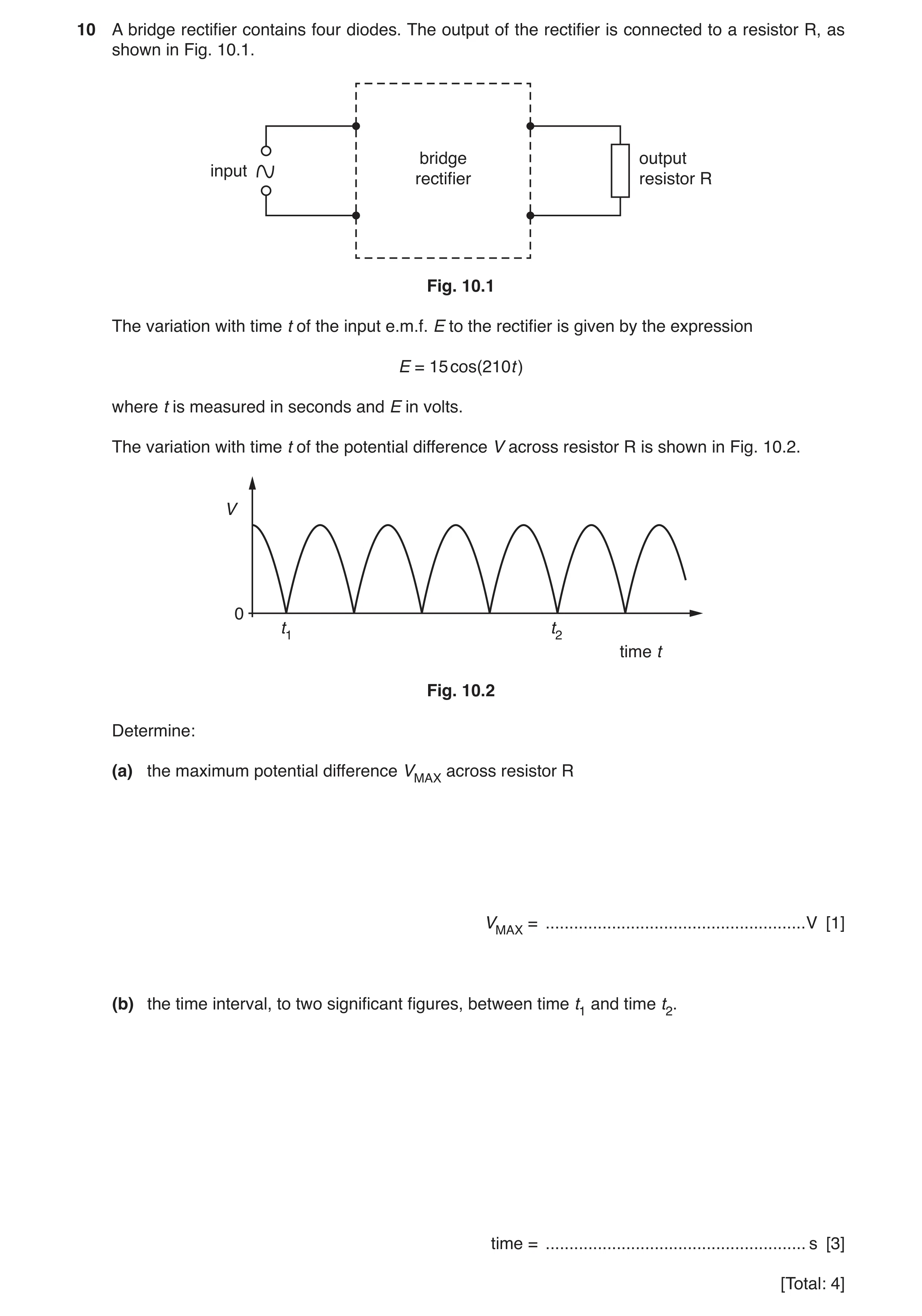
Q4 · A bridge rectifier contains four diodes 9702/41 May/June 2019
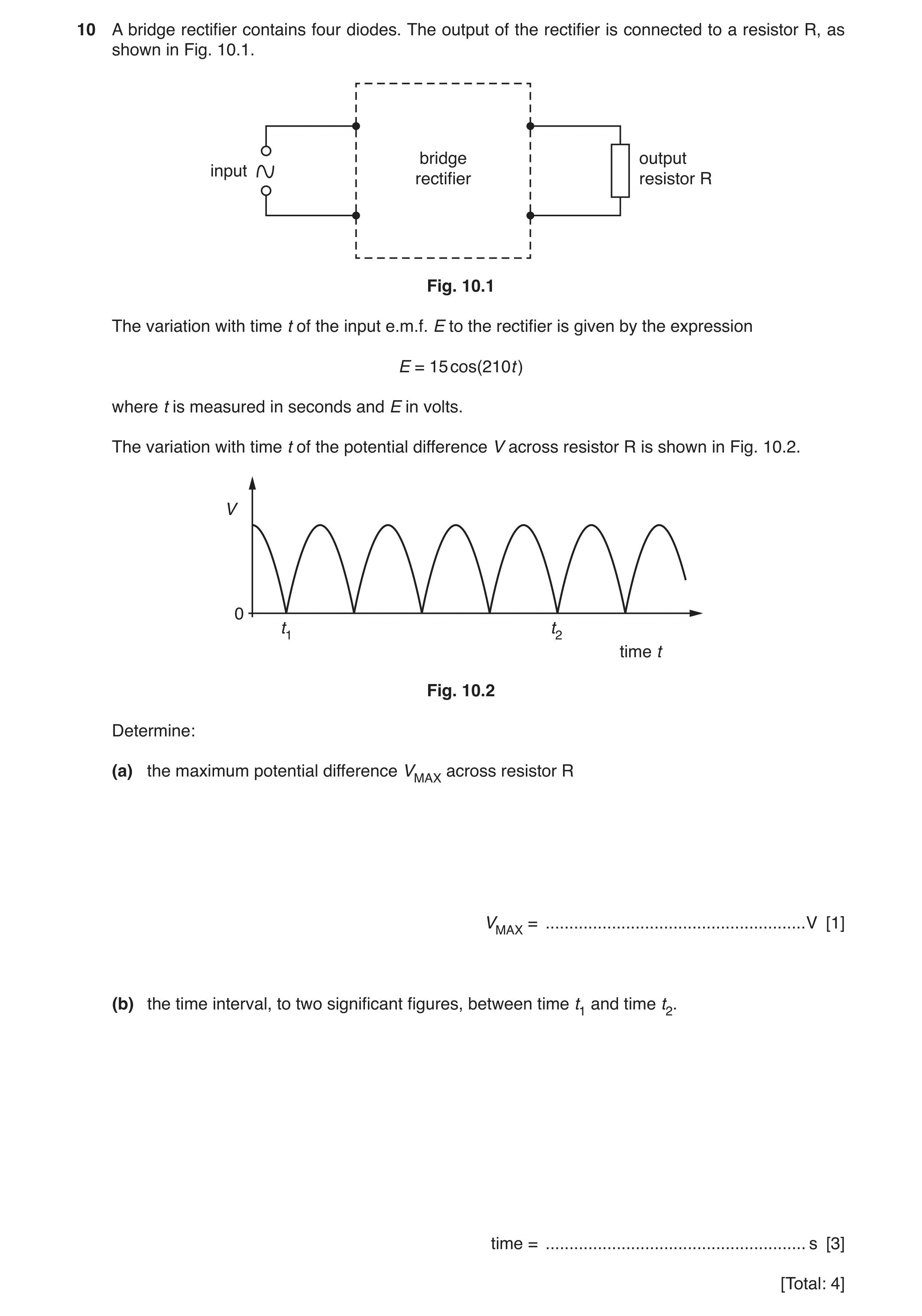
10 A bridge rectifier contains four diodes. The output of the rectifier is connected to a resistor R, as shown in Fig. 10.1. bridge output input rectifier resistor R Fig. 10.1 The variation with time t of the input e.m.f. E to the rectifier is given by the expression E = 15 cos(210t ) where t is measured in seconds and E in volts. The variation with time t of the potential difference V across resistor R is shown in Fig. 10.2. V 0 t1 t2 time t Fig. 10.2 Determine: (a) the maximum potential difference VMAX across resistor R VMAX = … V [1] (b) the time interval, to two significant figures, between time t1 and time t2. time = … s [3] [Total: 4]
4 marks
Mark scheme: 10(a) VMAX = 15 V A1 10(b) 210 = 2π / T C1 T = 0.0299 s C1 (t2 – t1) = 0.060 s A1
This question in 9702/41 May/June 2019
Q5 · A bridge rectifier contains four diodes 9702/43 May/June 2019
10 A bridge rectifier contains four diodes. The output of the rectifier is connected to a resistor R, as shown in Fig. 10.1. bridge output input rectifier resistor R Fig. 10.1 The variation with time t of the input e.m.f. E to the rectifier is given by the expression E = 15 cos(210t ) where t is measured in seconds and E in volts. The variation with time t of the potential difference V across resistor R is shown in Fig. 10.2. V 0 t1 t2 time t Fig. 10.2 Determine: (a) the maximum potential difference VMAX across resistor R VMAX = … V [1] (b) the time interval, to two significant figures, between time t1 and time t2. time = … s [3] [Total: 4]
4 marks
Mark scheme: 10(a) VMAX = 15 V A1 10(b) 210 = 2π / T C1 T = 0.0299 s C1 (t2 – t1) = 0.060 s A1
This question in 9702/43 May/June 2019
Q6 · A bridge rectifier using four ideal diodes is shown in Fig 9702/41 Oct/Nov 2019
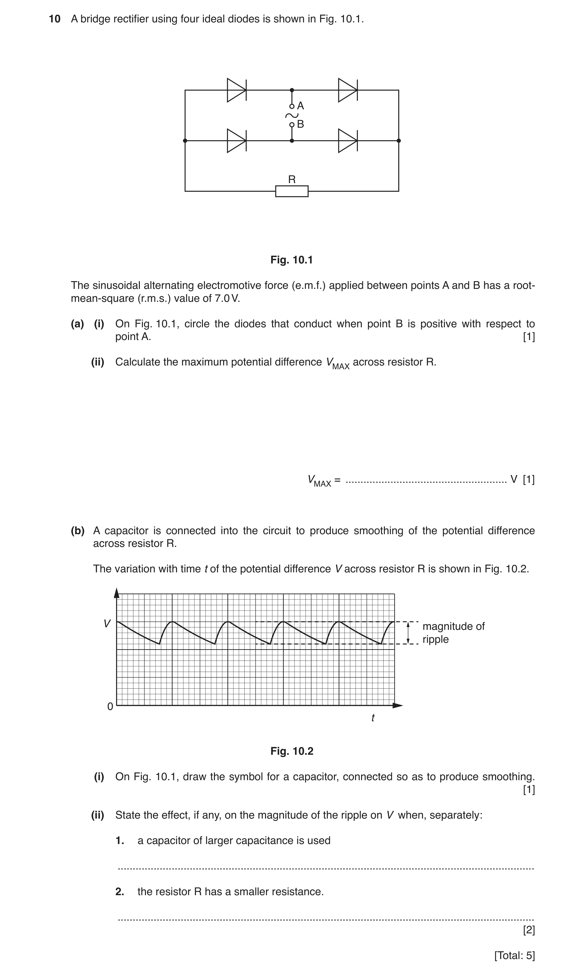
10 A bridge rectifier using four ideal diodes is shown in Fig. 10.1. A B R Fig. 10.1 The sinusoidal alternating electromotive force (e.m.f.) applied between points A and B has a root- mean-square (r.m.s.) value of 7.0 V. (a) (i) On Fig. 10.1, circle the diodes that conduct when point B is positive with respect to point A. [1] (ii) Calculate the maximum potential difference VMAX across resistor R. VMAX = … V [1] (b) A capacitor is connected into the circuit to produce smoothing of the potential difference across resistor R. The variation with time t of the potential difference V across resistor R is shown in Fig. 10.2. V magnitude of ripple 0 t Fig. 10.2 (i) On Fig. 10.1, draw the symbol for a capacitor, connected so as to produce smoothing. [1] (ii) State the effect, if any, on the magnitude of the ripple on V when, separately: 1. a capacitor of larger capacitance is used … 2. the resistor R has a smaller resistance. … [2] [Total: 5]
5 marks
Mark scheme: 10(a)(i) lower right and upper left diodes circled B1 10(a)(ii) maximum = 7.0√2 maximum = 9.9 V A1 10(b)(i) correct symbol for capacitor, shown connected in parallel with R B1 10(b)(ii) 1. (ripple) decreases B1 2. (ripple) increases B1
This question in 9702/41 Oct/Nov 2019
Q7 · A bridge rectifier using four ideal diodes is shown in Fig 9702/43 Oct/Nov 2019
10 A bridge rectifier using four ideal diodes is shown in Fig. 10.1. A B R Fig. 10.1 The sinusoidal alternating electromotive force (e.m.f.) applied between points A and B has a root- mean-square (r.m.s.) value of 7.0 V. (a) (i) On Fig. 10.1, circle the diodes that conduct when point B is positive with respect to point A. [1] (ii) Calculate the maximum potential difference VMAX across resistor R. VMAX = … V [1] (b) A capacitor is connected into the circuit to produce smoothing of the potential difference across resistor R. The variation with time t of the potential difference V across resistor R is shown in Fig. 10.2. V magnitude of ripple 0 t Fig. 10.2 (i) On Fig. 10.1, draw the symbol for a capacitor, connected so as to produce smoothing. [1] (ii) State the effect, if any, on the magnitude of the ripple on V when, separately: 1. a capacitor of larger capacitance is used … 2. the resistor R has a smaller resistance. … [2] [Total: 5]
5 marks
Mark scheme: 10(a)(i) lower right and upper left diodes circled B1 10(a)(ii) maximum = 7.0√2 maximum = 9.9 V A1 10(b)(i) correct symbol for capacitor, shown connected in parallel with R B1 10(b)(ii) 1. (ripple) decreases B1 2. (ripple) increases B1
This question in 9702/43 Oct/Nov 2019
Q8 · State two advantages of the transmission of data in digital, rather than analogue, form 9702/42 Oct/Nov 2020
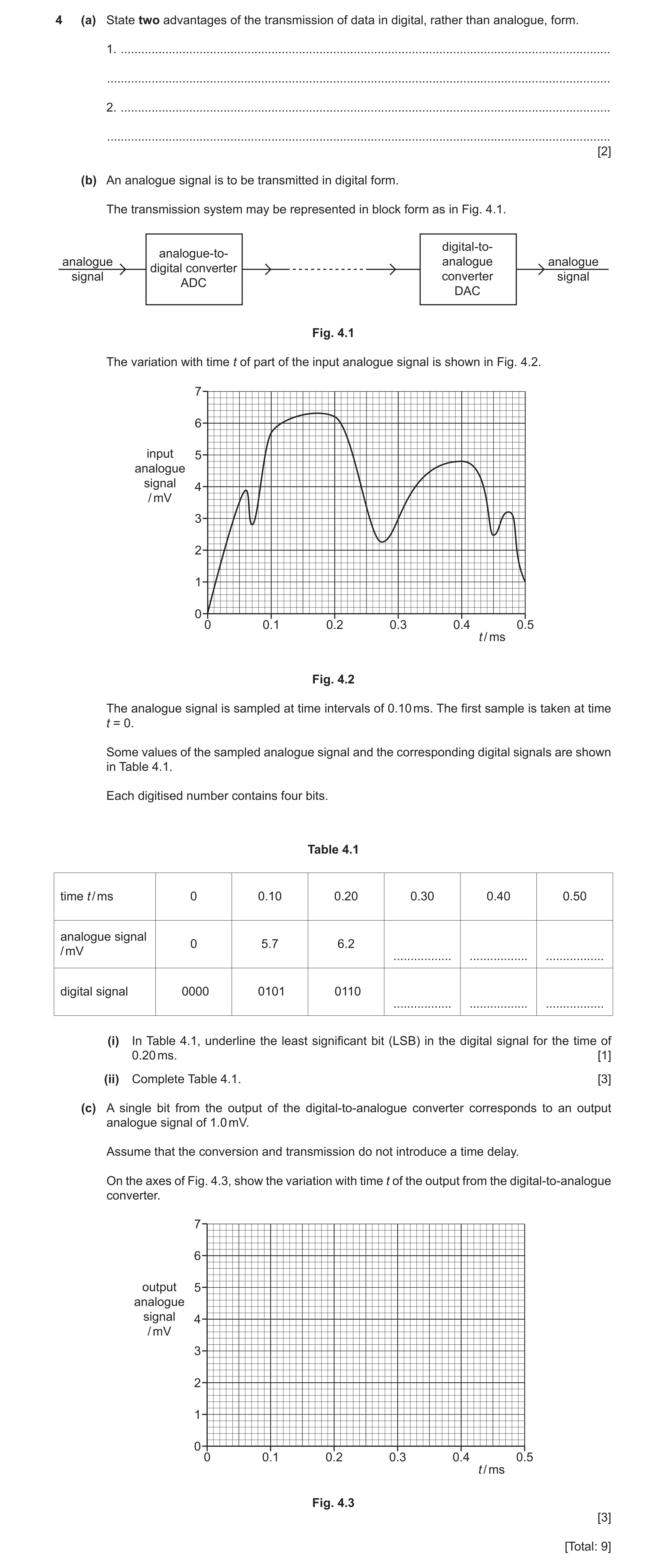
4 (a) State two advantages of the transmission of data in digital, rather than analogue, form. 1. … … 2. … … [2] (b) An analogue signal is to be transmitted in digital form. The transmission system may be represented in block form as in Fig. 4.1. digital-to- analogue-to- analogue analogue analogue digital converter signal converter signal ADC DAC Fig. 4.1 The variation with time t of part of the input analogue signal is shown in Fig. 4.2. 7 6 input 5 analogue signal 4 / mV 3 2 1 0 0 0.1 0.2 0.3 0.4 0.5 t / ms Fig. 4.2 The analogue signal is sampled at time intervals of 0.10 ms. The first sample is taken at time t = 0. Some values of the sampled analogue signal and the corresponding digital signals are shown in Table 4.1. Each digitised number contains four bits. Table 4.1 time t / ms 0 0.10 0.20 0.30 0.40 0.50 analogue signal 0 5.7 6.2/ mV … … … digital signal 0000 0101 0110 … … … (i) In Table 4.1, underline the least significant bit (LSB) in the digital signal for the time of 0.20 ms. [1] (ii) Complete Table 4.1. [3] (c) A single bit from the output of the digital-to-analogue converter corresponds to an output analogue signal of 1.0 mV. Assume that the conversion and transmission do not introduce a time delay. On the axes of Fig. 4.3, show the variation with time t of the output from the digital-to-analogue converter. 7 6 output 5 analogue signal 4 / mV 3 2 1 0 0 0.1 0.2 0.3 0.4 0.5 t / ms Fig. 4.3 [3] [Total: 9]
9 marks
Mark scheme: 4(a) any two points from: • signal can be regenerated/noise can be removed • signal can be encrypted • signal can be checked for errors • multiplexing is possible • circuits are more reliable/cheaper • data can be transmitted at a greater rate B2 4(b)(i) right-hand zero underlined (0110) B1 4(b)(ii) analogue signals given as: 3.0, 4.8, 1.0 B1 0011 at 0.30 ms and 0001 at 0.50 ms B1 0100 at 0.40 ms B1 4(c) series of steps, all of width 0.1 ms B1 steps levels, in order, at output voltage 0, 5, 6, 3 and 4 mV 2 marks: all levels correct 1 mark: one level incorrect and all others correct or one level omitted and last step shown at 1 mV B2
This question in 9702/42 Oct/Nov 2020
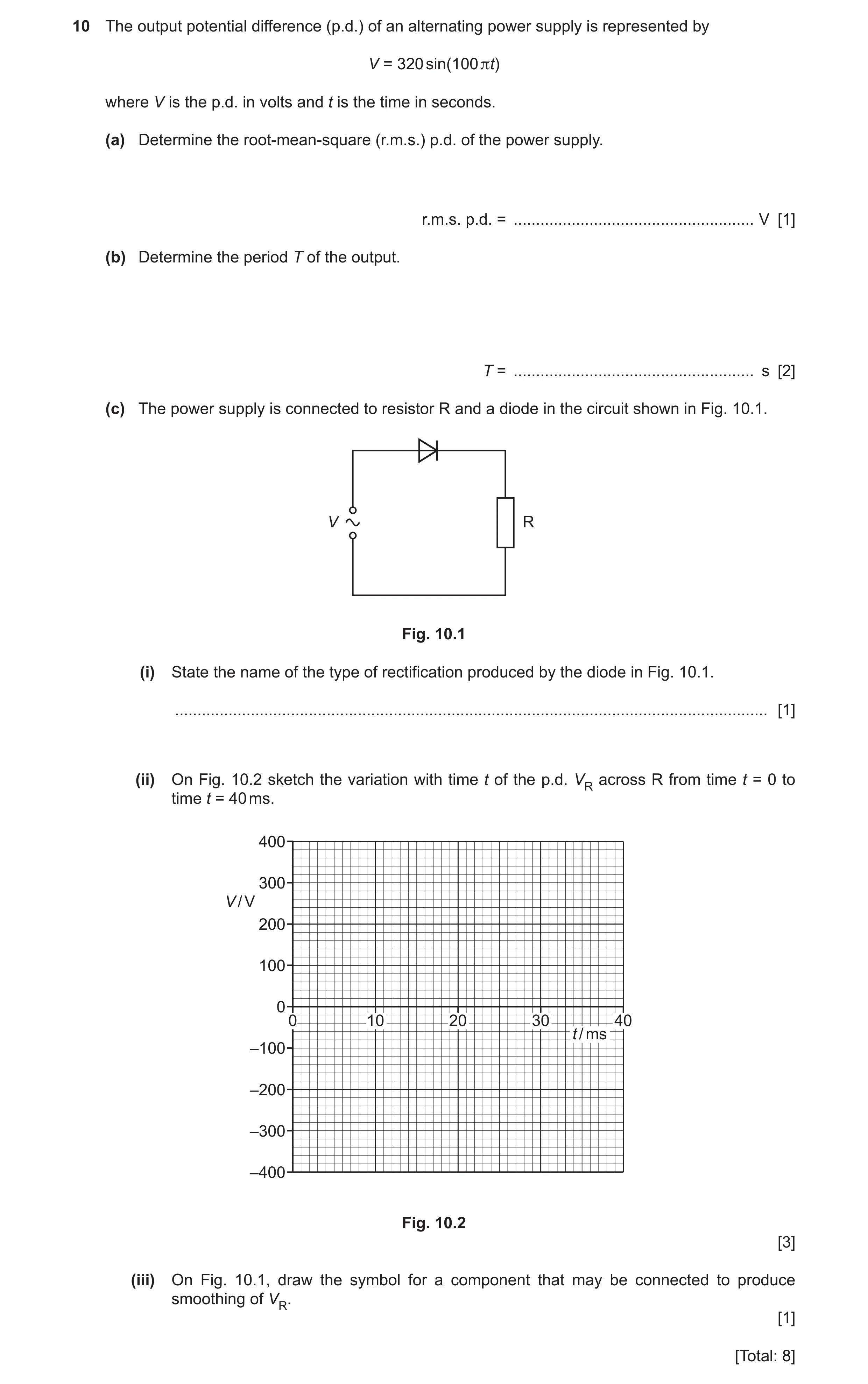
Q9 · The output potential difference (p.d.) of an alternating power supply is represented by V… 9702/42 Feb/March 2021
10 The output potential difference (p.d.) of an alternating power supply is represented by V = 320 sin(100 πt) where V is the p.d. in volts and t is the time in seconds. (a) Determine the root-mean-square (r.m.s.) p.d. of the power supply. r.m.s. p.d. = … V [1] (b) Determine the period T of the output. T = … s [2] (c) The power supply is connected to resistor R and a diode in the circuit shown in Fig. 10.1. V R Fig. 10.1 (i) State the name of the type of rectification produced by the diode in Fig. 10.1. … [1] (ii) On Fig. 10.2 sketch the variation with time t of the p.d. VR across R from time t = 0 to time t = 40 ms. 400 300 V / V 200 100 0 0 10 20 30 40 t / ms –100 –200 –300 –400 Fig. 10.2 [3] (iii) On Fig. 10.1, draw the symbol for a component that may be connected to produce smoothing of VR. [1] [Total: 8]
8 marks
Mark scheme: 10(a) 230 V A1 10(b) ω = 100π 2 2 100 T π π ω π = = C1 0.020 s = A1 10(c)(i) half-wave (rectification) B1 10(c)(ii) sinusoidal half waves in positive V only or negative V only, peak at 320 V B1 line at zero for second half of cycle B1 two time periods shown, each of 0.020 s B1 10(c)(iii) capacitor added in parallel with resistor B1
This question in 9702/42 Feb/March 2021
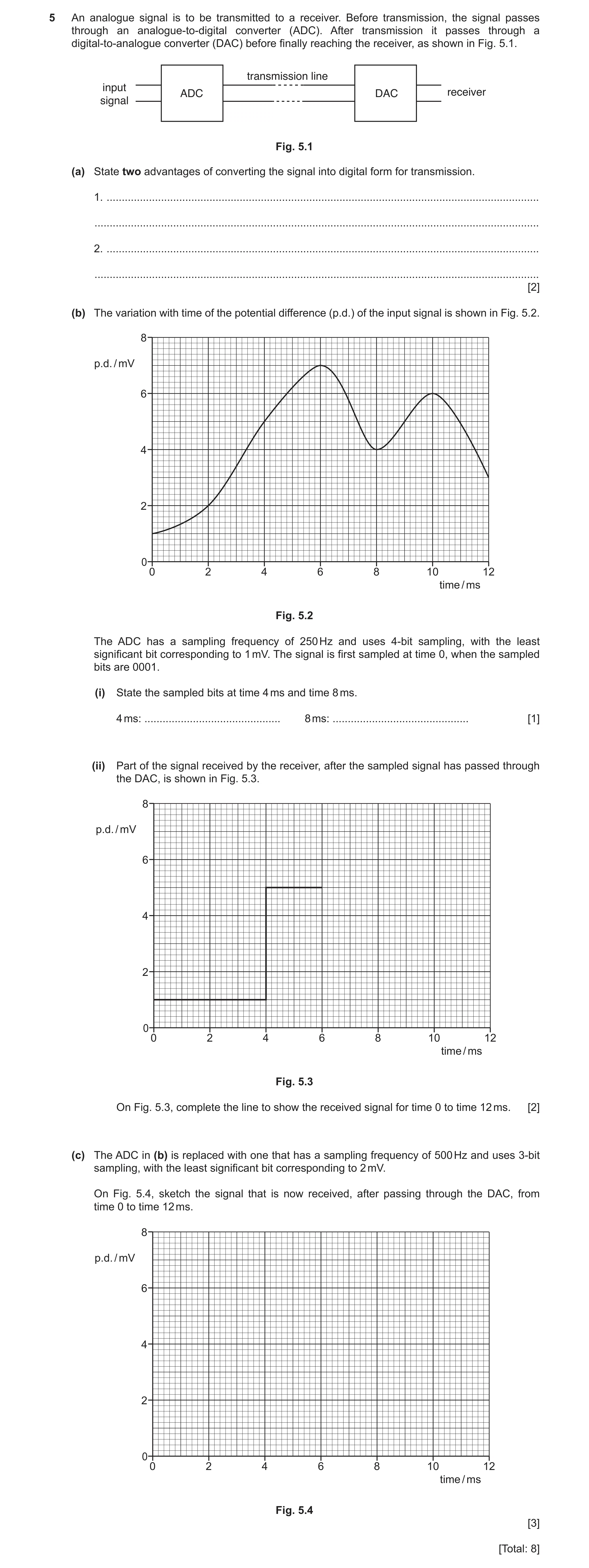
Q10 · An analogue signal is to be transmitted to a receiver 9702/41 Oct/Nov 2021
5 An analogue signal is to be transmitted to a receiver. Before transmission, the signal passes through an analogue-to-digital converter (ADC). After transmission it passes through a digital-to-analogue converter (DAC) before finally reaching the receiver, as shown in Fig. 5.1. transmission line input ADC DAC receiver signal Fig. 5.1 (a) State two advantages of converting the signal into digital form for transmission. 1. … … 2. … … [2] (b) The variation with time of the potential difference (p.d.) of the input signal is shown in Fig. 5.2. 8 p.d. / mV 6 4 2 0 0 2 4 6 8 10 12 time / ms Fig. 5.2 The ADC has a sampling frequency of 250 Hz and uses 4-bit sampling, with the least significant bit corresponding to 1 mV. The signal is first sampled at time 0, when the sampled bits are 0001. (i) State the sampled bits at time 4 ms and time 8 ms. 4 ms: … 8 ms: … [1] (ii) Part of the signal received by the receiver, after the sampled signal has passed through the DAC, is shown in Fig. 5.3. 8 p.d. / mV 6 4 2 0 0 2 4 6 8 10 12 time / ms Fig. 5.3 On Fig. 5.3, complete the line to show the received signal for time 0 to time 12 ms. [2] (c) The ADC in (b) is replaced with one that has a sampling frequency of 500 Hz and uses 3-bit sampling, with the least significant bit corresponding to 2 mV. On Fig. 5.4, sketch the signal that is now received, after passing through the DAC, from time 0 to time 12 ms. 8 p.d. / mV 6 4 2 0 0 2 4 6 8 10 12 time / ms Fig. 5.4 [3] [Total: 8]
8 marks
Mark scheme: 5(a) • noise can be removed/signal can be regenerated • extra bits can be added for error-checking • signal can be encrypted (for increased security) • data compression/multiplexing is possible Any two points, 1 mark each B2 5(b)(i) 4 ms: 0101 and 8 ms: 0100 B1 5(b)(ii) sketch: horizontal line continues to 8 ms, then new horizontal line from 8 ms to 12 ms B1 level of line after 8 ms is 4 mV B1 5(c) sketch: series of steps of width 2 ms B1 step heights at 0, 2, 4, 6, 4, 6 mV 2 marks if all correct, 1 mark if only one incorrect B2
This question in 9702/41 Oct/Nov 2021
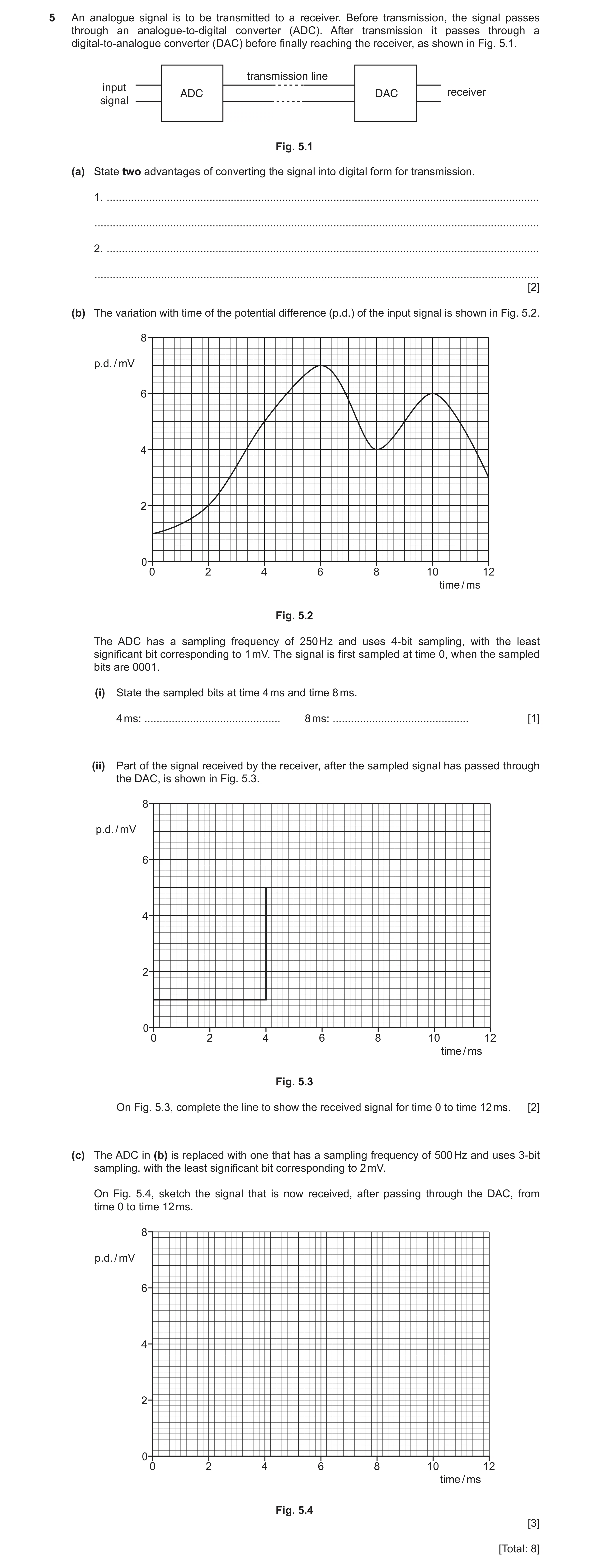
Q11 · An analogue signal is to be transmitted to a receiver 9702/43 Oct/Nov 2021
5 An analogue signal is to be transmitted to a receiver. Before transmission, the signal passes through an analogue-to-digital converter (ADC). After transmission it passes through a digital-to-analogue converter (DAC) before finally reaching the receiver, as shown in Fig. 5.1. transmission line input ADC DAC receiver signal Fig. 5.1 (a) State two advantages of converting the signal into digital form for transmission. 1. … … 2. … … [2] (b) The variation with time of the potential difference (p.d.) of the input signal is shown in Fig. 5.2. 8 p.d. / mV 6 4 2 0 0 2 4 6 8 10 12 time / ms Fig. 5.2 The ADC has a sampling frequency of 250 Hz and uses 4-bit sampling, with the least significant bit corresponding to 1 mV. The signal is first sampled at time 0, when the sampled bits are 0001. (i) State the sampled bits at time 4 ms and time 8 ms. 4 ms: … 8 ms: … [1] (ii) Part of the signal received by the receiver, after the sampled signal has passed through the DAC, is shown in Fig. 5.3. 8 p.d. / mV 6 4 2 0 0 2 4 6 8 10 12 time / ms Fig. 5.3 On Fig. 5.3, complete the line to show the received signal for time 0 to time 12 ms. [2] (c) The ADC in (b) is replaced with one that has a sampling frequency of 500 Hz and uses 3-bit sampling, with the least significant bit corresponding to 2 mV. On Fig. 5.4, sketch the signal that is now received, after passing through the DAC, from time 0 to time 12 ms. 8 p.d. / mV 6 4 2 0 0 2 4 6 8 10 12 time / ms Fig. 5.4 [3] [Total: 8]
8 marks
Mark scheme: 5(a) • noise can be removed/signal can be regenerated • extra bits can be added for error-checking • signal can be encrypted (for increased security) • data compression/multiplexing is possible Any two points, 1 mark each B2 5(b)(i) 4 ms: 0101 and 8 ms: 0100 B1 5(b)(ii) sketch: horizontal line continues to 8 ms, then new horizontal line from 8 ms to 12 ms B1 level of line after 8 ms is 4 mV B1 5(c) sketch: series of steps of width 2 ms B1 step heights at 0, 2, 4, 6, 4, 6 mV 2 marks if all correct, 1 mark if only one incorrect B2
This question in 9702/43 Oct/Nov 2021
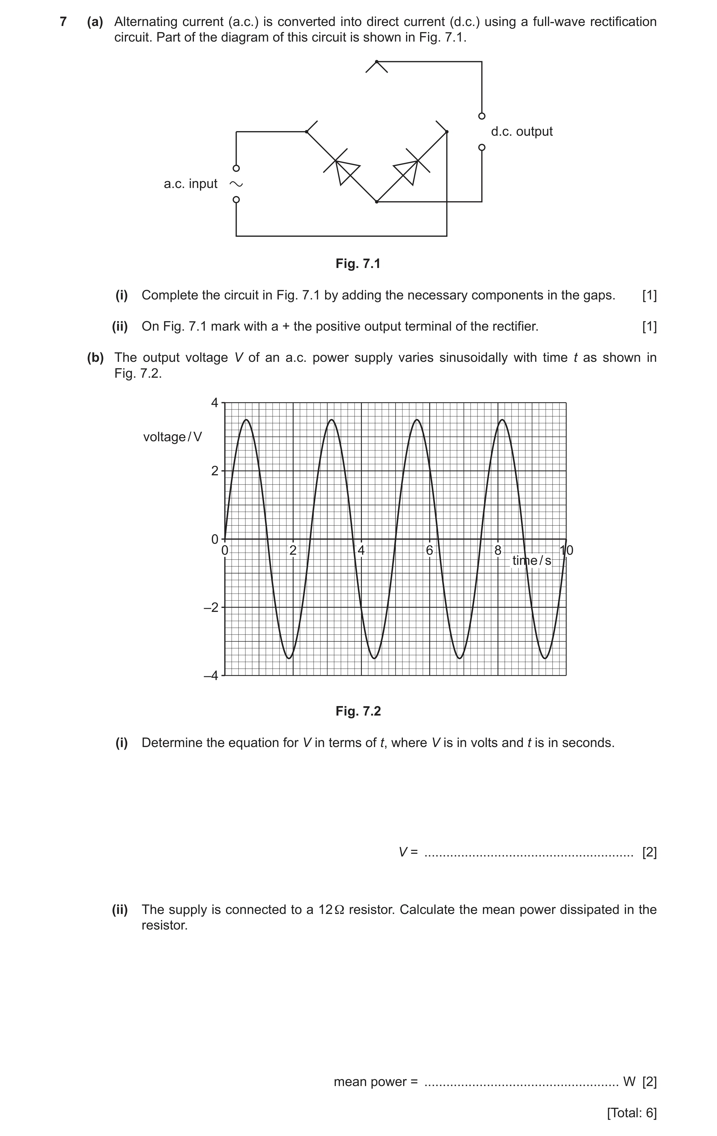
Q12 · Alternating current (a.c.) is converted into direct current (d.c.) using a full-wave… 9702/42 Feb/March 2022
7 (a) Alternating current (a.c.) is converted into direct current (d.c.) using a full-wave rectification circuit. Part of the diagram of this circuit is shown in Fig. 7.1. d.c. output a.c. input Fig. 7.1 (i) Complete the circuit in Fig. 7.1 by adding the necessary components in the gaps. [1] (ii) On Fig. 7.1 mark with a + the positive output terminal of the rectifier. [1] (b) The output voltage V of an a.c. power supply varies sinusoidally with time t as shown in Fig. 7.2. 4 voltage / V 2 0 0 2 4 6 8 10 time / s –2 –4 Fig. 7.2 (i) Determine the equation for V in terms of t, where V is in volts and t is in seconds. V = … [2] (ii) The supply is connected to a 12 Ω resistor. Calculate the mean power dissipated in the resistor. mean power = … W [2] [Total: 6]
6 marks
Mark scheme: 7(a)(i) two diodes added in correct directions (Both diodes pointing inwards and upwards), correct symbols only B1 7(a)(ii) ‘+’ anywhere on upper output wire B1 7(b)(i) ω = 2π / T = 2π / 2.5 = 0.80 π or 4π / 5 or 2.5 C1 (V =) 3.5 sin (0.8π t) or 3.5 sin (4π t / 5) or 3.5 sin (2.5 t) A1 Question Answer Marks 7(b)(ii) 2 V (P=) 2R or 2 . . . (P=) R r m s V 2 3.5 = 2 12 × or 2 2.47 12 C1 = 0.51 W A1
This question in 9702/42 Feb/March 2022
Q13 · Four diodes and a load resistor of resistance 1.2 kΩ, connected in a circuit that is used… 9702/41 May/June 2022
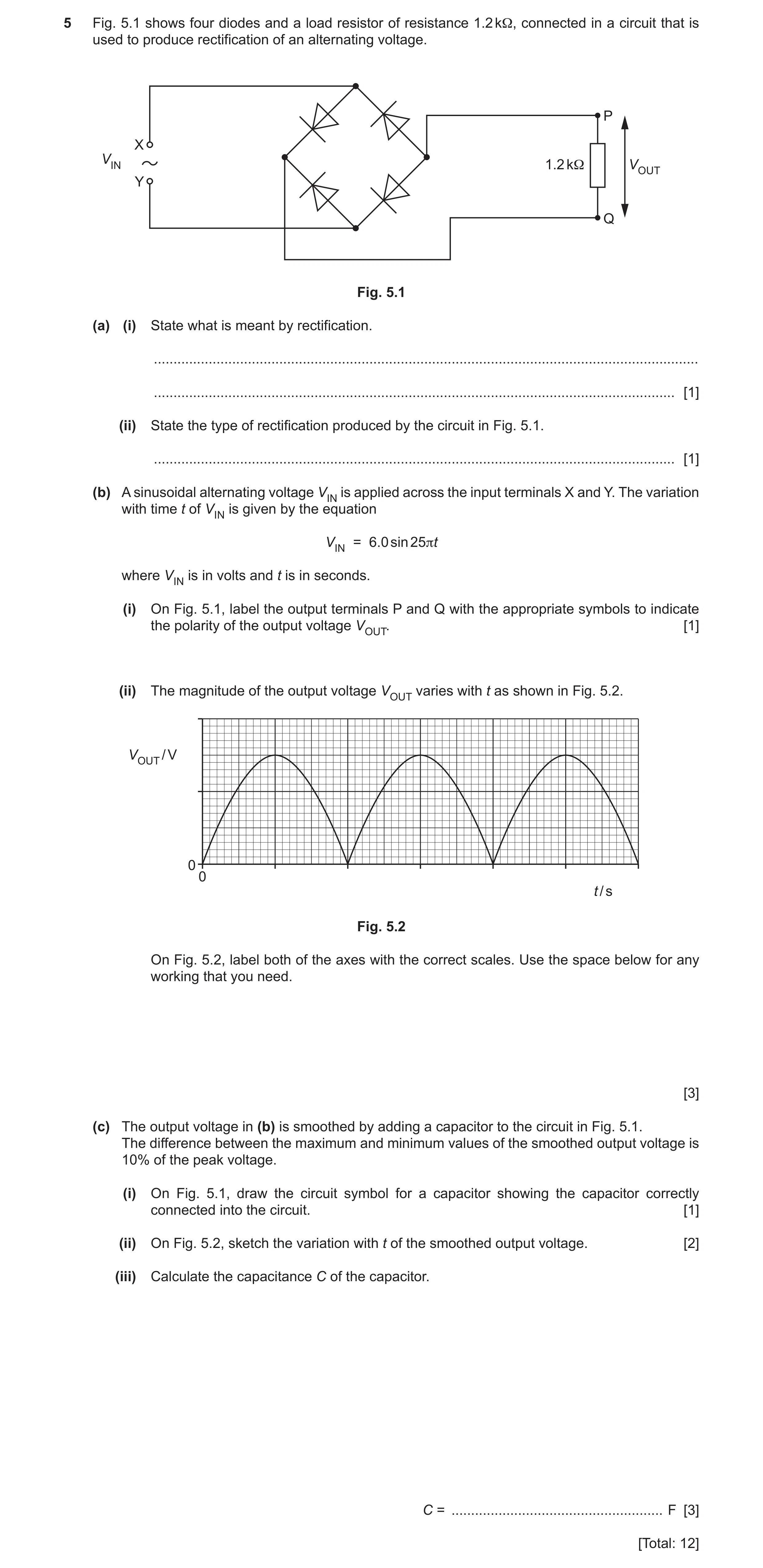
5 Fig. 5.1 shows four diodes and a load resistor of resistance 1.2 kΩ, connected in a circuit that is used to produce rectification of an alternating voltage. P X VIN 1.2 kΩ VOUT Y Q Fig. 5.1 (a) (i) State what is meant by rectification. … … [1] (ii) State the type of rectification produced by the circuit in Fig. 5.1. … [1] (b) A sinusoidal alternating voltage VIN is applied across the input terminals X and Y. The variation with time t of VIN is given by the equation VIN = 6.0 sin 25πt where VIN is in volts and t is in seconds. (i) On Fig. 5.1, label the output terminals P and Q with the appropriate symbols to indicate the polarity of the output voltage VOUT. [1] (ii) The magnitude of the output voltage VOUT varies with t as shown in Fig. 5.2. VOUT / V 0 0 t / s Fig. 5.2 On Fig. 5.2, label both of the axes with the correct scales. Use the space below for any working that you need. [3] (c) The output voltage in (b) is smoothed by adding a capacitor to the circuit in Fig. 5.1. The difference between the maximum and minimum values of the smoothed output voltage is 10% of the peak voltage. (i) On Fig. 5.1, draw the circuit symbol for a capacitor showing the capacitor correctly connected into the circuit. [1] (ii) On Fig. 5.2, sketch the variation with t of the smoothed output voltage. [2] (iii) Calculate the capacitance C of the capacitor. C = … F [3] [Total: 12]
12 marks
Mark scheme: 5(a)(i) conversion (from a.c.) to d.c. B1 5(a)(ii) full-wave (rectification) B1 5(b)(i) P labelled – and Q labelled + B1 5(b)(ii) VOUT scale labelled 4 and 8 on the 2 cm tick marks B1 T = 2 / = 2 / 25 = 0.08 s C1 t scale labelled 0.02, 0.04, 0.06, 0.08, 0.10, 0.12 on the 2 cm tick marks A1 5(c)(i) correct symbol used for capacitor and capacitor connected in parallel with the 1.2 k resistor. B1 5(c)(ii) straight lines or curves, with negative decreasing gradients, drawn between adjacent peaks, from top of first peak to meet line going up to next peak B1 lines, from one peak to the line going up to the next peak, show a drop in p.d. of 1½ small squares B1 5(c)(iii) V = 0.90 6.0 (= 5.4 V) or discharge time (for each cycle) = 0.034 s C1 V = V0 exp (– t / RC) 5.4 = 6.0 exp [– 0.034 / (1.2 103 C)] C1 C = 2.7 10–4 F A1
This question in 9702/41 May/June 2022
Q14 · Four diodes and a load resistor of resistance 1.2 kΩ, connected in a circuit that is used… 9702/43 May/June 2022
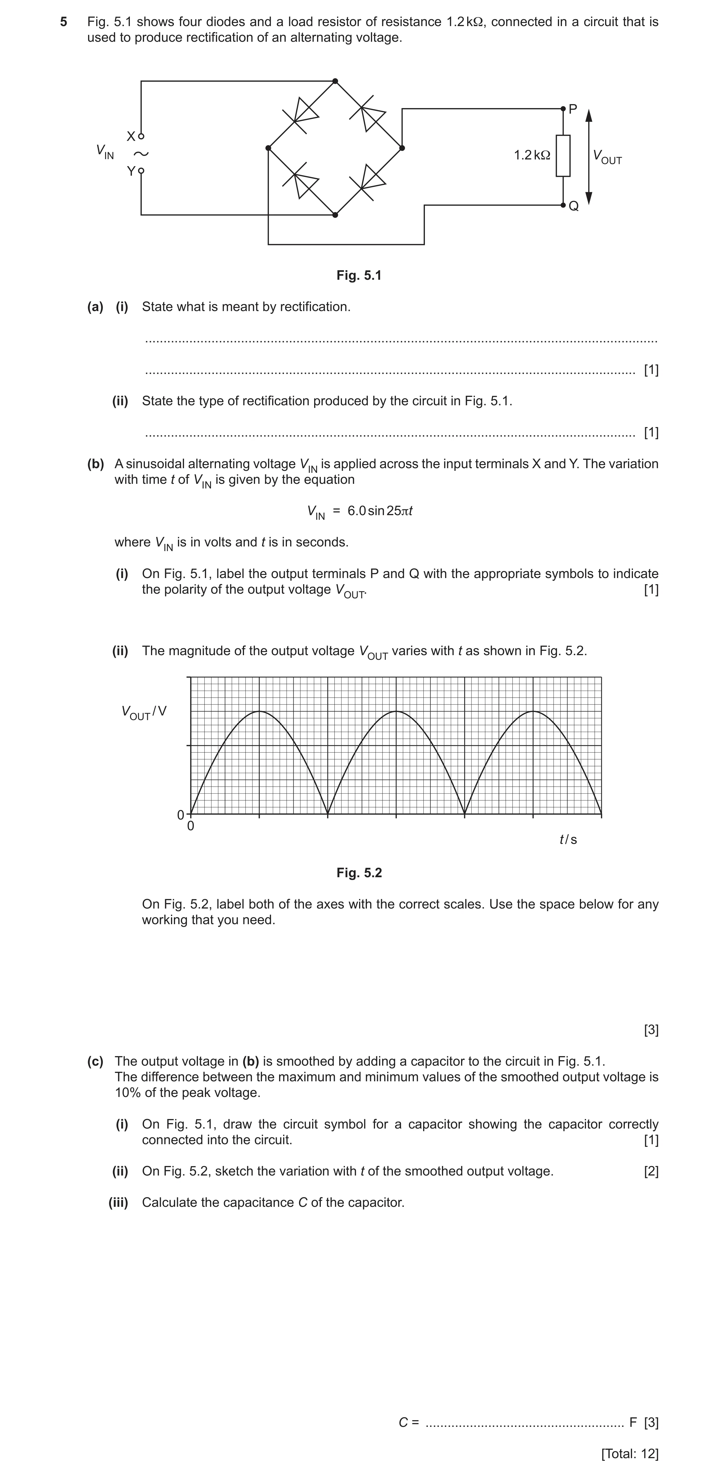
5 Fig. 5.1 shows four diodes and a load resistor of resistance 1.2 kΩ, connected in a circuit that is used to produce rectification of an alternating voltage. P X VIN 1.2 kΩ VOUT Y Q Fig. 5.1 (a) (i) State what is meant by rectification. … … [1] (ii) State the type of rectification produced by the circuit in Fig. 5.1. … [1] (b) A sinusoidal alternating voltage VIN is applied across the input terminals X and Y. The variation with time t of VIN is given by the equation VIN = 6.0 sin 25πt where VIN is in volts and t is in seconds. (i) On Fig. 5.1, label the output terminals P and Q with the appropriate symbols to indicate the polarity of the output voltage VOUT. [1] (ii) The magnitude of the output voltage VOUT varies with t as shown in Fig. 5.2. VOUT / V 0 0 t / s Fig. 5.2 On Fig. 5.2, label both of the axes with the correct scales. Use the space below for any working that you need. [3] (c) The output voltage in (b) is smoothed by adding a capacitor to the circuit in Fig. 5.1. The difference between the maximum and minimum values of the smoothed output voltage is 10% of the peak voltage. (i) On Fig. 5.1, draw the circuit symbol for a capacitor showing the capacitor correctly connected into the circuit. [1] (ii) On Fig. 5.2, sketch the variation with t of the smoothed output voltage. [2] (iii) Calculate the capacitance C of the capacitor. C = … F [3] [Total: 12]
12 marks
Mark scheme: 5(a)(i) conversion (from a.c.) to d.c. B1 5(a)(ii) full-wave (rectification) B1 5(b)(i) P labelled – and Q labelled + B1 5(b)(ii) VOUT scale labelled 4 and 8 on the 2 cm tick marks B1 T = 2 / = 2 / 25 = 0.08 s C1 t scale labelled 0.02, 0.04, 0.06, 0.08, 0.10, 0.12 on the 2 cm tick marks A1 5(c)(i) correct symbol used for capacitor and capacitor connected in parallel with the 1.2 k resistor. B1 5(c)(ii) straight lines or curves, with negative decreasing gradients, drawn between adjacent peaks, from top of first peak to meet line going up to next peak B1 lines, from one peak to the line going up to the next peak, show a drop in p.d. of 1½ small squares B1 5(c)(iii) V = 0.90 6.0 (= 5.4 V) or discharge time (for each cycle) = 0.034 s C1 V = V0 exp (– t / RC) 5.4 = 6.0 exp [– 0.034 / (1.2 103 C)] C1 C = 2.7 10–4 F A1
This question in 9702/43 May/June 2022
Q15 · Part of an electric circuit is shown in Fig 9702/41 May/June 2023
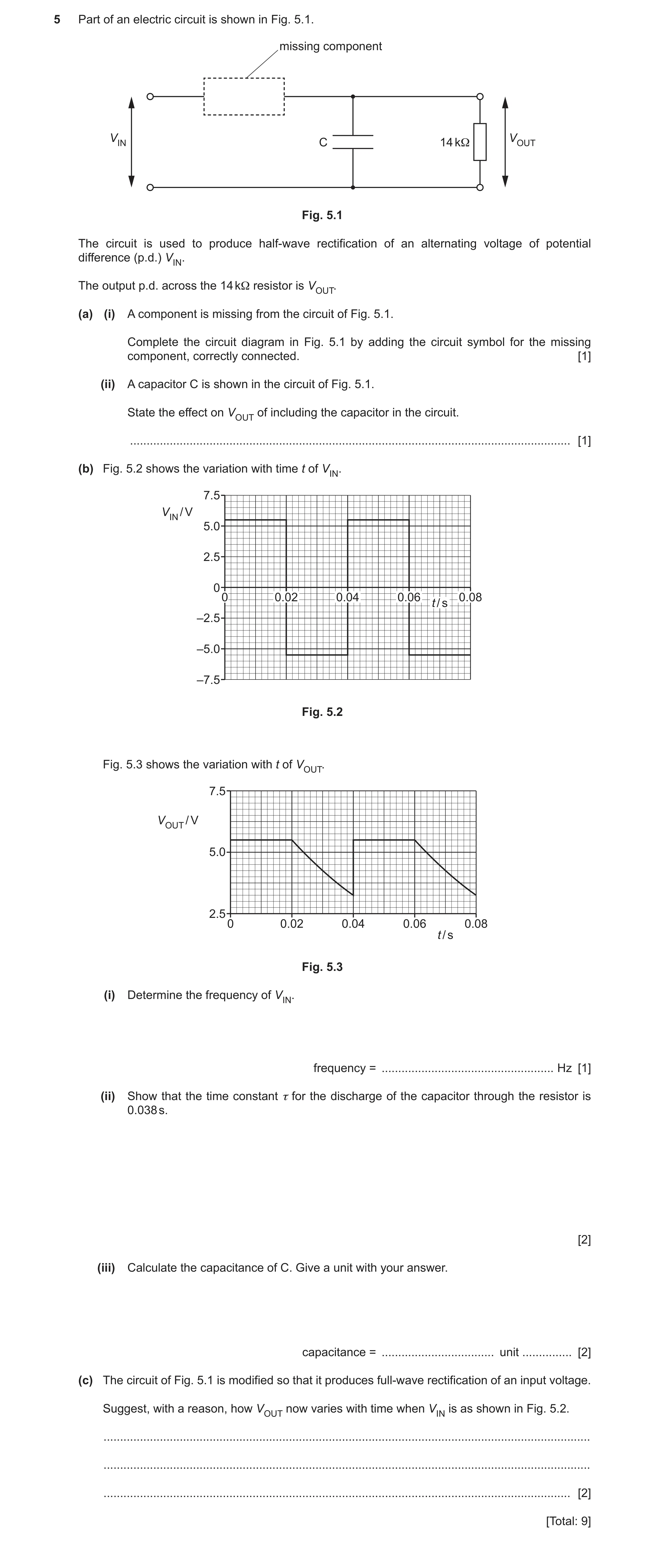
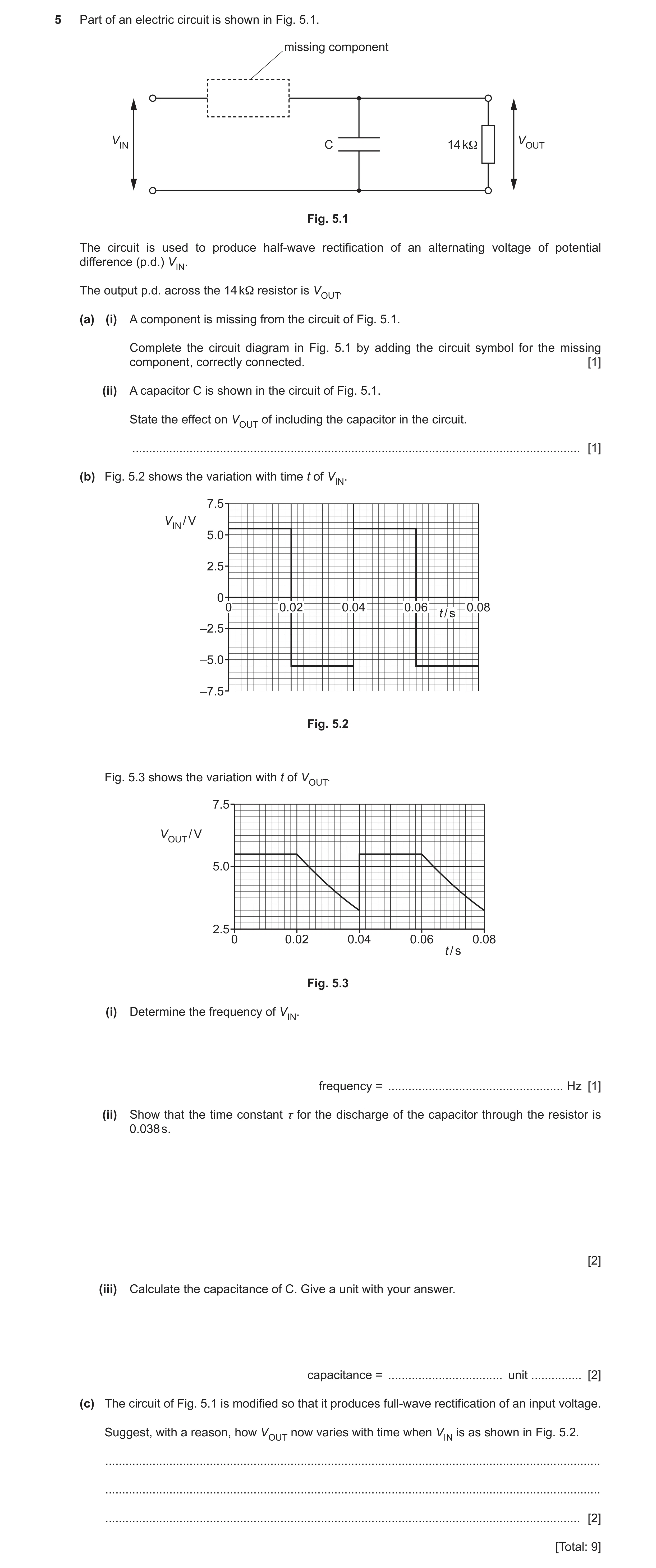
5 Part of an electric circuit is shown in Fig. 5.1. missing component VIN C 14 kΩ VOUT Fig. 5.1 The circuit is used to produce half-wave rectification of an alternating voltage of potential difference (p.d.) VIN. The output p.d. across the 14 kΩ resistor is VOUT. (a) (i) A component is missing from the circuit of Fig. 5.1. Complete the circuit diagram in Fig. 5.1 by adding the circuit symbol for the missing component, correctly connected. [1] (ii) A capacitor C is shown in the circuit of Fig. 5.1. State the effect on VOUT of including the capacitor in the circuit. … [1] (b) Fig. 5.2 shows the variation with time t of VIN. 7.5 VIN / V 5.0 2.5 0 0 0.02 0.04 0.06 0.08 t / s –2.5 –5.0 –7.5 Fig. 5.2 Fig. 5.3 shows the variation with t of VOUT. 7.5 VOUT / V 5.0 2.5 0 0.02 0.04 0.06 0.08 t / s Fig. 5.3 (i) Determine the frequency of VIN. frequency = … Hz [1] (ii) Show that the time constant τ for the discharge of the capacitor through the resistor is 0.038 s. [2] (iii) Calculate the capacitance of C. Give a unit with your answer. capacitance = … unit … [2] (c) The circuit of Fig. 5.1 is modified so that it produces full-wave rectification of an input voltage. Suggest, with a reason, how VOUT now varies with time when VIN is as shown in Fig. 5.2. … … … [2] [Total: 9]
9 marks
Mark scheme: 5(a)(i) correct circuit symbol for a diode shown correctly connected in series with the wires leading into and out of the dotted box B1 5(a)(ii) smoothing / VOUT is smoothed B1 5(b)(i) frequency = 1 / 0.04 = 25 Hz A1 5(b)(ii) V = V0 exp (– t / RC) and = RC or V = V0 exp (– t / ) C1 3.25 = 5.50 exp (– 0.020 / ) leading to = 0.038 s A1 5(b)(iii) = RC C1 capacitance = 0.038 / 14000 = 2.7 10–6 F A1 5(c) VIN has constant magnitude in both positive and negative directions B1 (so) VOUT is (now) constant / VOUT does not vary with time B1
This question in 9702/41 May/June 2023
Q16 · Four diodes are used in a bridge rectifier circuit to produce rectification of a… 9702/42 May/June 2023
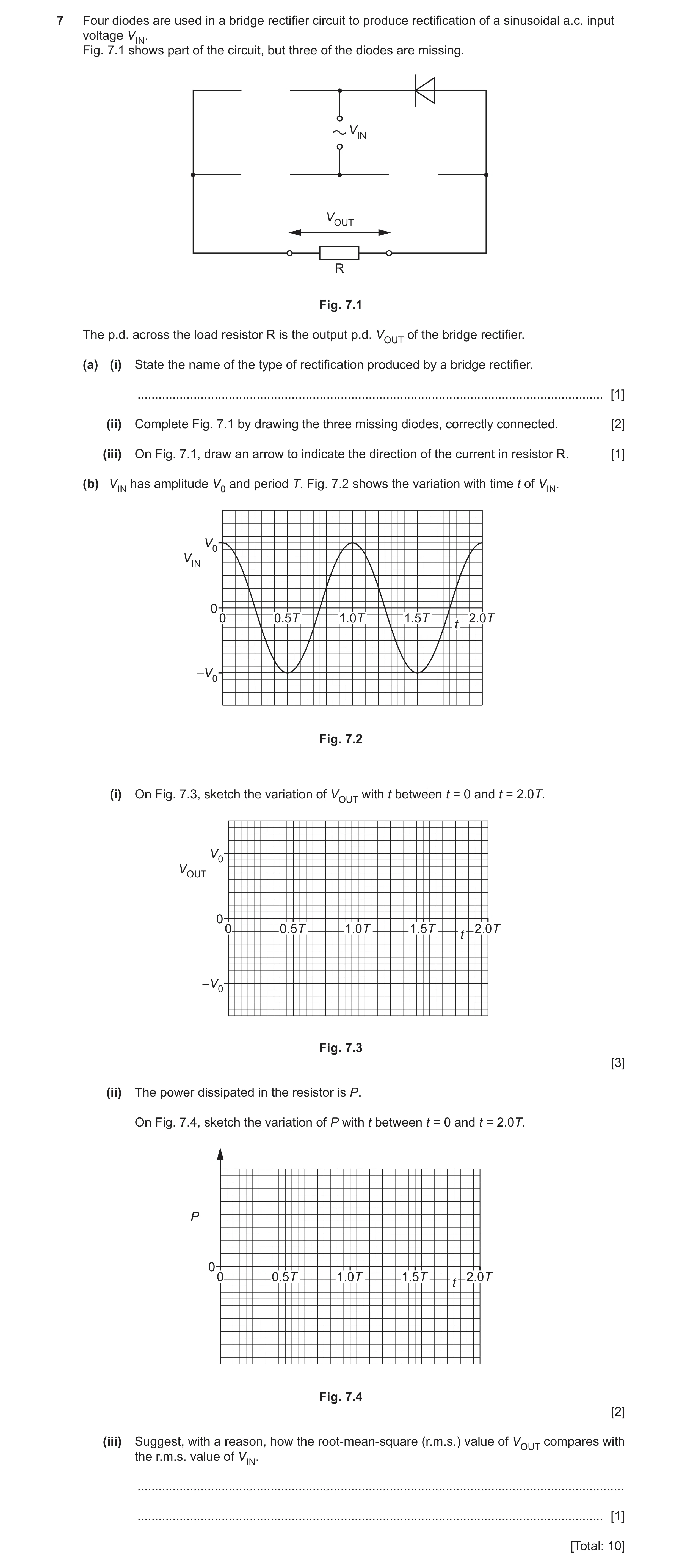
7 Four diodes are used in a bridge rectifier circuit to produce rectification of a sinusoidal a.c. input voltage VIN. Fig. 7.1 shows part of the circuit, but three of the diodes are missing. VIN VOUT R Fig. 7.1 The p.d. across the load resistor R is the output p.d. VOUT of the bridge rectifier. (a) (i) State the name of the type of rectification produced by a bridge rectifier. … [1] (ii) Complete Fig. 7.1 by drawing the three missing diodes, correctly connected. [2] (iii) On Fig. 7.1, draw an arrow to indicate the direction of the current in resistor R. [1] (b) VIN has amplitude V0 and period T. Fig. 7.2 shows the variation with time t of VIN. V0 VIN 0 0 0.5T 1.0T 1.5T 2.0T t –V0 Fig. 7.2 (i) On Fig. 7.3, sketch the variation of VOUT with t between t = 0 and t = 2.0T. V0 VOUT 0 0 0.5T 1.0T 1.5T 2.0T t –V0 Fig. 7.3 [3] (ii) The power dissipated in the resistor is P. On Fig. 7.4, sketch the variation of P with t between t = 0 and t = 2.0T. P 0 0 0.5T 1.0T 1.5T 2.0T t Fig. 7.4 [2] (iii) Suggest, with a reason, how the root-mean-square (r.m.s.) value of VOUT compares with the r.m.s. value of VIN. … … [1] [Total: 10]
10 marks
Mark scheme: 7(a)(i) full-wave (rectification) B1 7(a)(ii) lower left diode shown pointing left B1 lower right and upper left diodes shown pointing left B1 7(a)(iii) arrow indicating current direction in resistor to the right B1 7(b)(i) sketch: periodic line showing minimum VOUT = 0 and maximum VOUT = +V0 B1 line showing peak VOUT at t = 0, 0.5T, 1.0T, 1.5T and 2.0T, with VOUT going to zero half-way in between each peak B1 line showing correct modulated sine shape B1 7(b)(ii) sketch: sinusoidal curve with troughs sitting on the time axis B1 peak power at t = 0, 0.5T, 1.0T, 1.5T and 2.0T and zero power half-way in between each peak B1 7(b)(iii) same power-time graph with or without rectification, so same Vrms or V2-time graph is same for both VOUT and VIN, so same Vrms or power does not depend on sign of V, so same Vrms B1
This question in 9702/42 May/June 2023
Q17 · Part of an electric circuit is shown in Fig 9702/43 May/June 2023
5 Part of an electric circuit is shown in Fig. 5.1. missing component VIN C 14 kΩ VOUT Fig. 5.1 The circuit is used to produce half-wave rectification of an alternating voltage of potential difference (p.d.) VIN. The output p.d. across the 14 kΩ resistor is VOUT. (a) (i) A component is missing from the circuit of Fig. 5.1. Complete the circuit diagram in Fig. 5.1 by adding the circuit symbol for the missing component, correctly connected. [1] (ii) A capacitor C is shown in the circuit of Fig. 5.1. State the effect on VOUT of including the capacitor in the circuit. … [1] (b) Fig. 5.2 shows the variation with time t of VIN. 7.5 VIN / V 5.0 2.5 0 0 0.02 0.04 0.06 0.08 t / s –2.5 –5.0 –7.5 Fig. 5.2 Fig. 5.3 shows the variation with t of VOUT. 7.5 VOUT / V 5.0 2.5 0 0.02 0.04 0.06 0.08 t / s Fig. 5.3 (i) Determine the frequency of VIN. frequency = … Hz [1] (ii) Show that the time constant τ for the discharge of the capacitor through the resistor is 0.038 s. [2] (iii) Calculate the capacitance of C. Give a unit with your answer. capacitance = … unit … [2] (c) The circuit of Fig. 5.1 is modified so that it produces full-wave rectification of an input voltage. Suggest, with a reason, how VOUT now varies with time when VIN is as shown in Fig. 5.2. … … … [2] [Total: 9]
9 marks
Mark scheme: 5(a)(i) correct circuit symbol for a diode shown correctly connected in series with the wires leading into and out of the dotted box B1 5(a)(ii) smoothing / VOUT is smoothed B1 5(b)(i) frequency = 1 / 0.04 = 25 Hz A1 5(b)(ii) V = V0 exp (– t / RC) and = RC or V = V0 exp (– t / ) C1 3.25 = 5.50 exp (– 0.020 / ) leading to = 0.038 s A1 5(b)(iii) = RC C1 capacitance = 0.038 / 14000 = 2.7 10–6 F A1 5(c) VIN has constant magnitude in both positive and negative directions B1 (so) VOUT is (now) constant / VOUT does not vary with time B1
This question in 9702/43 May/June 2023
Q18 · A circuit contains a power supply that provides a sinusoidal alternating input voltage VIN 9702/41 May/June 2024
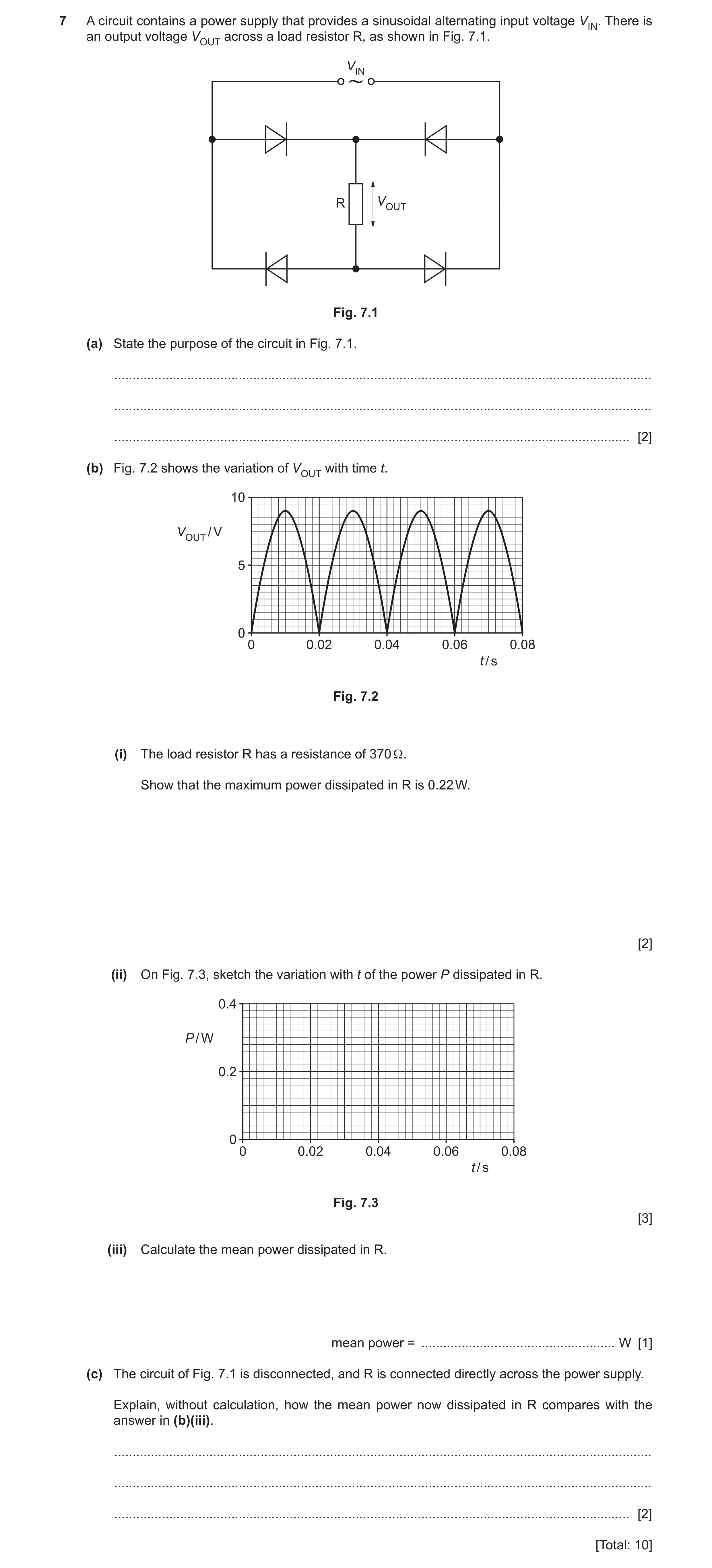
7 A circuit contains a power supply that provides a sinusoidal alternating input voltage VIN. There is an output voltage VOUT across a load resistor R, as shown in Fig. 7.1. VIN R VOUT Fig. 7.1 (a) State the purpose of the circuit in Fig. 7.1. … … … [2] (b) Fig. 7.2 shows the variation of VOUT with time t. 10 VOUT / V 5 0 0 0.02 0.04 0.06 0.08 t / s Fig. 7.2 (i) The load resistor R has a resistance of 370 Ω. Show that the maximum power dissipated in R is 0.22 W. [2] (ii) On Fig. 7.3, sketch the variation with t of the power P dissipated in R. 0.4 P / W 0.2 0 0 0.02 0.04 0.06 0.08 t / s Fig. 7.3 [3] (iii) Calculate the mean power dissipated in R. mean power = … W [1] (c) The circuit of Fig. 7.1 is disconnected, and R is connected directly across the power supply. Explain, without calculation, how the mean power now dissipated in R compares with the answer in (b)(iii). … … … [2] [Total: 10]
10 marks
Mark scheme: 7(a) rectification (of the input voltage) M1 full-wave A1 7(b)(i) P = V2 / R or maximum V = 9.0 V C1 PMAX = 9.02 / 370 = 0.22 W A1 7(b)(ii) sinusoidal shape with minima sitting on the time axis B1 correct frequency and phase, with minima at 0, 0.02, 0.04, 0.06 and 0.08 s and maxima at 0.01, 0.03, 0.05 and 0.07 s B1 all maxima shown at 0.22 W B1 7(b)(iii) mean power = peak power / 2 = 0.22 / 2 = 0.11 W A1 7(c) power–time graph is identical B1 (so) mean powers are equal B1
This question in 9702/41 May/June 2024
Q19 · A circuit contains a power supply that provides a sinusoidal alternating input voltage VIN 9702/43 May/June 2024
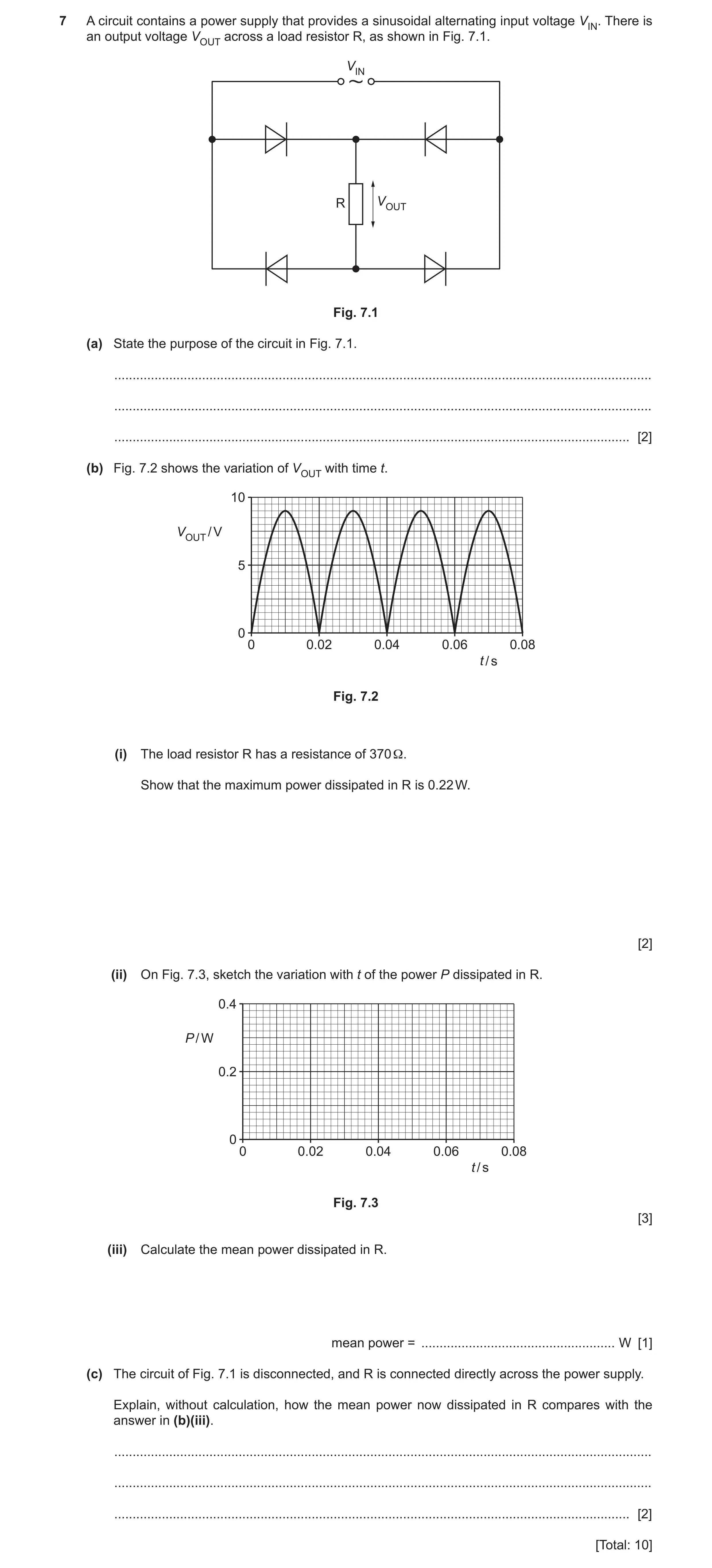
7 A circuit contains a power supply that provides a sinusoidal alternating input voltage VIN. There is an output voltage VOUT across a load resistor R, as shown in Fig. 7.1. VIN R VOUT Fig. 7.1 (a) State the purpose of the circuit in Fig. 7.1. … … … [2] (b) Fig. 7.2 shows the variation of VOUT with time t. 10 VOUT / V 5 0 0 0.02 0.04 0.06 0.08 t / s Fig. 7.2 (i) The load resistor R has a resistance of 370 Ω. Show that the maximum power dissipated in R is 0.22 W. [2] (ii) On Fig. 7.3, sketch the variation with t of the power P dissipated in R. 0.4 P / W 0.2 0 0 0.02 0.04 0.06 0.08 t / s Fig. 7.3 [3] (iii) Calculate the mean power dissipated in R. mean power = … W [1] (c) The circuit of Fig. 7.1 is disconnected, and R is connected directly across the power supply. Explain, without calculation, how the mean power now dissipated in R compares with the answer in (b)(iii). … … … [2] [Total: 10]
10 marks
Mark scheme: 7(a) rectification (of the input voltage) M1 full-wave A1 7(b)(i) P = V2 / R or maximum V = 9.0 V C1 PMAX = 9.02 / 370 = 0.22 W A1 7(b)(ii) sinusoidal shape with minima sitting on the time axis B1 correct frequency and phase, with minima at 0, 0.02, 0.04, 0.06 and 0.08 s and maxima at 0.01, 0.03, 0.05 and 0.07 s B1 all maxima shown at 0.22 W B1 7(b)(iii) mean power = peak power / 2 = 0.22 / 2 = 0.11 W A1 7(c) power–time graph is identical B1 (so) mean powers are equal B1
This question in 9702/43 May/June 2024
Q20 · State what is meant by rectification of an alternating voltage 9702/41 Oct/Nov 2024
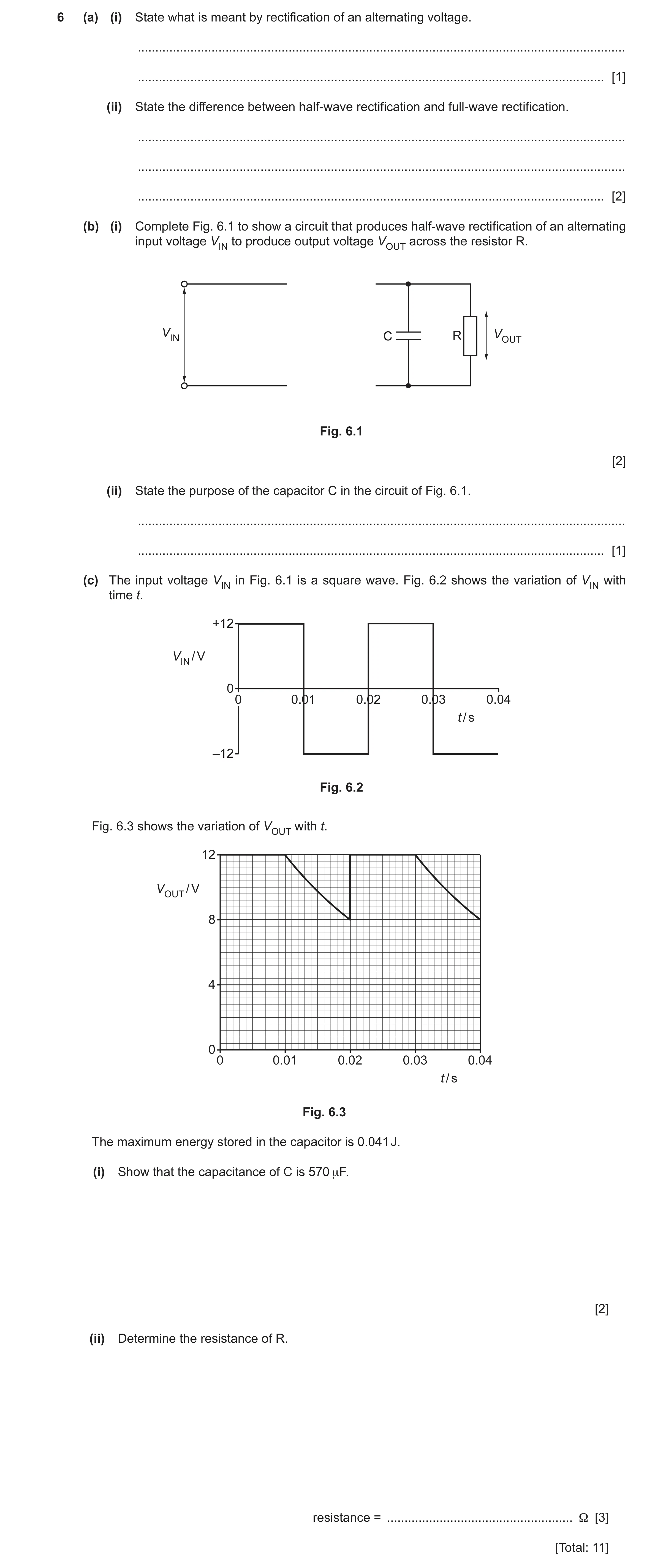
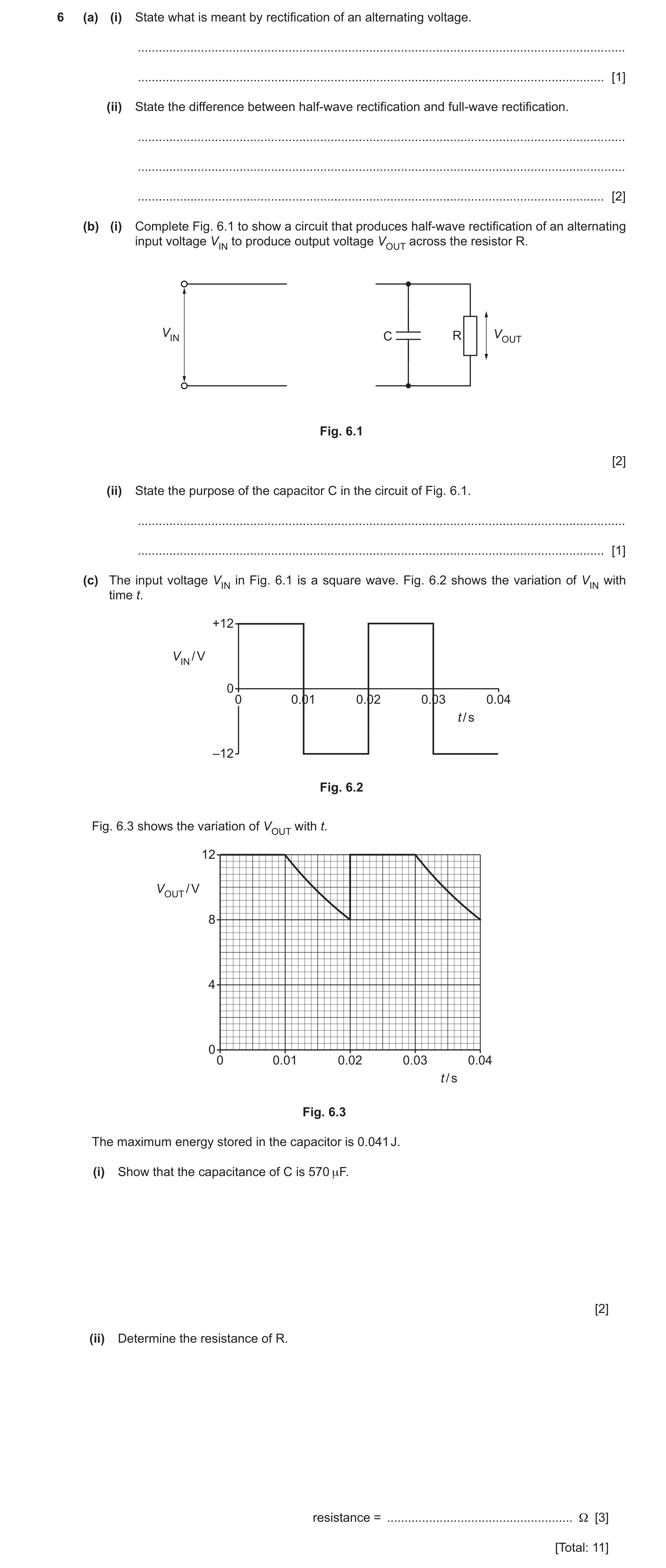
6 (a) (i) State what is meant by rectification of an alternating voltage. … … [1] (ii) State the difference between half-wave rectification and full-wave rectification. … … … [2] (b) (i) Complete Fig. 6.1 to show a circuit that produces half-wave rectification of an alternating input voltage VIN to produce output voltage VOUT across the resistor R. VIN C R VOUT Fig. 6.1 [2] (ii) State the purpose of the capacitor C in the circuit of Fig. 6.1. … … [1] (c) The input voltage VIN in Fig. 6.1 is a square wave. Fig. 6.2 shows the variation of VIN with time t. +12 VIN / V 0 0 0.01 0.02 0.03 0.04 t / s –12 Fig. 6.2 Fig. 6.3 shows the variation of VOUT with t. 12 VOUT / V 8 4 0 0 0.01 0.02 0.03 0.04 t / s Fig. 6.3 The maximum energy stored in the capacitor is 0.041 J. (i) Show that the capacitance of C is 570 μF. [2] (ii) Determine the resistance of R. resistance = … Ω [3] [Total: 11]
11 marks
Mark scheme: 6(a)(i) conversion (from a.c.) to d.c. B1 6(a)(ii) half-wave: voltage in one direction is removed B1 full-wave: voltage in one direction is reversed B1 6(b)(i) one gap connected by a single diode and other gap connected directly B1 diode drawn (in a circuit) with correct circuit symbol B1 6(b)(ii) smoothing B1 6(c)(i) E = ½CV2 C1 C = 2 0.041 / 122 = 5.7 10–4 F = 570 F A1 6(c)(ii) 8.0 = 12.0 exp (– 0.010 / RC) C1 ln (8.0 / 12.0) = – 0.010 / (R 5.7 10–4) C1 R = 43 A1
This question in 9702/41 Oct/Nov 2024
Q21 · State what is meant by rectification of an alternating voltage 9702/43 Oct/Nov 2024
6 (a) (i) State what is meant by rectification of an alternating voltage. … … [1] (ii) State the difference between half-wave rectification and full-wave rectification. … … … [2] (b) (i) Complete Fig. 6.1 to show a circuit that produces half-wave rectification of an alternating input voltage VIN to produce output voltage VOUT across the resistor R. VIN C R VOUT Fig. 6.1 [2] (ii) State the purpose of the capacitor C in the circuit of Fig. 6.1. … … [1] (c) The input voltage VIN in Fig. 6.1 is a square wave. Fig. 6.2 shows the variation of VIN with time t. +12 VIN / V 0 0 0.01 0.02 0.03 0.04 t / s –12 Fig. 6.2 Fig. 6.3 shows the variation of VOUT with t. 12 VOUT / V 8 4 0 0 0.01 0.02 0.03 0.04 t / s Fig. 6.3 The maximum energy stored in the capacitor is 0.041 J. (i) Show that the capacitance of C is 570 μF. [2] (ii) Determine the resistance of R. resistance = … Ω [3] [Total: 11]
11 marks
Mark scheme: 6(a)(i) conversion (from a.c.) to d.c. B1 6(a)(ii) half-wave: voltage in one direction is removed B1 full-wave: voltage in one direction is reversed B1 6(b)(i) one gap connected by a single diode and other gap connected directly B1 diode drawn (in a circuit) with correct circuit symbol B1 6(b)(ii) smoothing B1 6(c)(i) E = ½CV2 C1 C = 2 0.041 / 122 = 5.7 10–4 F = 570 F A1 6(c)(ii) 8.0 = 12.0 exp (– 0.010 / RC) C1 ln (8.0 / 12.0) = – 0.010 / (R 5.7 10–4) C1 R = 43 A1
This question in 9702/43 Oct/Nov 2024
Q22 · A circuit that rectifies an alternating input voltage VIN and produces an output voltage… 9702/41 May/June 2025
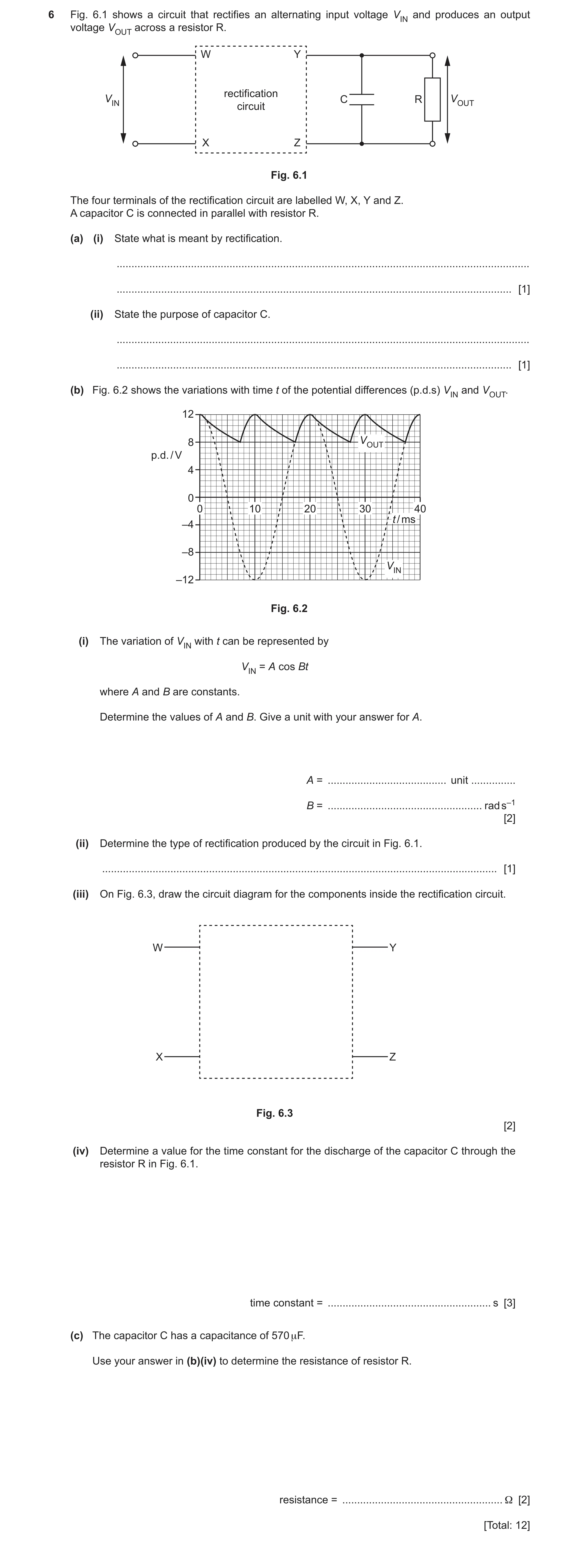
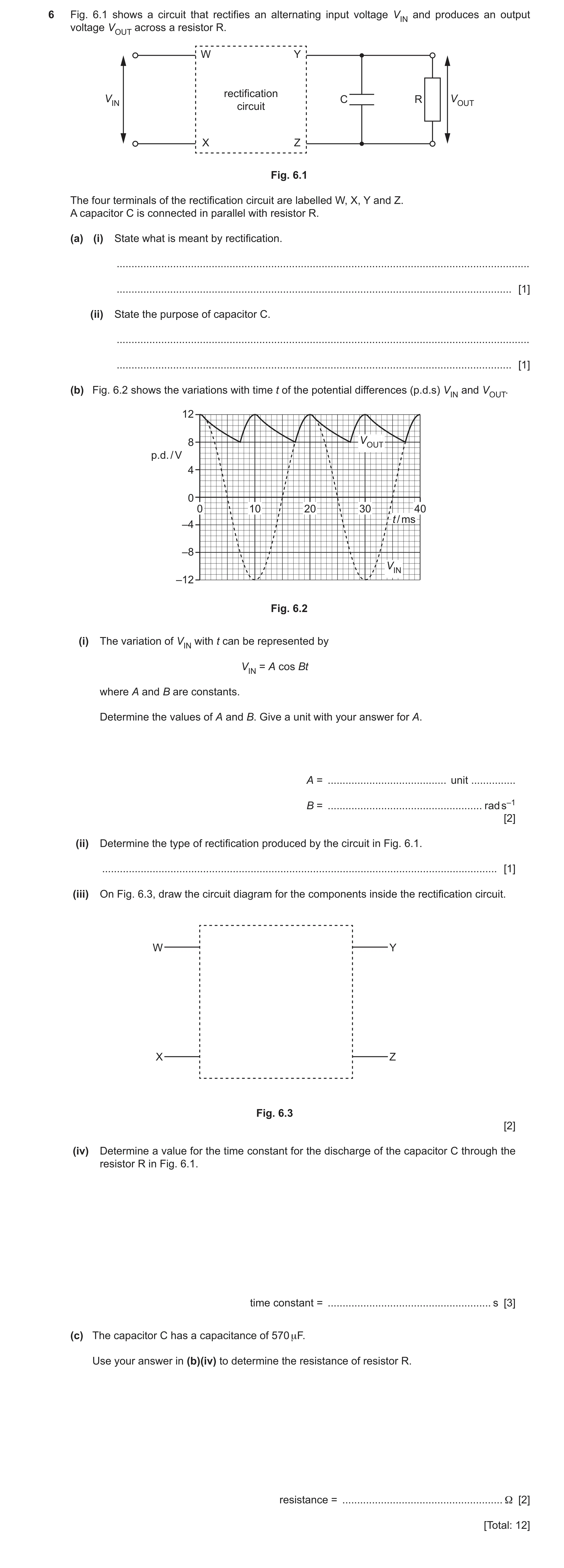
6 Fig. 6.1 shows a circuit that rectifies an alternating input voltage VIN and produces an output voltage VOUT across a resistor R. W Y rectification VIN C R VOUT circuit X Z Fig. 6.1 The four terminals of the rectification circuit are labelled W, X, Y and Z. A capacitor C is connected in parallel with resistor R. (a) (i) State what is meant by rectification. … … [1] (ii) State the purpose of capacitor C. … … [1] (b) Fig. 6.2 shows the variations with time t of the potential differences (p.d.s) VIN and VOUT. 12 8 VOUT p.d. / V 4 0 0 10 20 30 40 t / ms –4 –8 VIN –12 Fig. 6.2 (i) The variation of VIN with t can be represented by VIN = A cos Bt where A and B are constants. Determine the values of A and B. Give a unit with your answer for A. A = … unit … B = … rad s–1 [2] (ii) Determine the type of rectification produced by the circuit in Fig. 6.1. … [1] (iii) On Fig. 6.3, draw the circuit diagram for the components inside the rectification circuit. W Y X Z Fig. 6.3 [2] (iv) Determine a value for the time constant for the discharge of the capacitor C through the resistor R in Fig. 6.1. time constant = … s [3] (c) The capacitor C has a capacitance of 570 μF. Use your answer in (b)(iv) to determine the resistance of resistor R. resistance = … Ω [2] [Total: 12]
12 marks
Mark scheme: 6(a)(i) conversion from a.c. to d.c. B1 6(a)(ii) smoothing B1 6(b)(i) A = 12 V A1 B = 2 / (20 × 10–3) A1 = 310 rad s–1 6(b)(ii) full-wave (rectification) B1 6(b)(iii) four diodes shown, with correct circuit symbols B1 four diodes correctly connected to form a bridge rectifier B1 6(b)(iv) V = V0 exp (–t / ) C1 or V = V0 exp (–t / RC) and = RC 8.0 = 12 exp (– 7.3 × 10⁻³ / ) C1 = 0.018 s A1 6(c) time constant = RC C1 R = (0.018 / 570 × 10–6) A1 = 32
This question in 9702/41 May/June 2025
Q23 · A circuit that produces rectification of an alternating input voltage 9702/42 May/June 2025
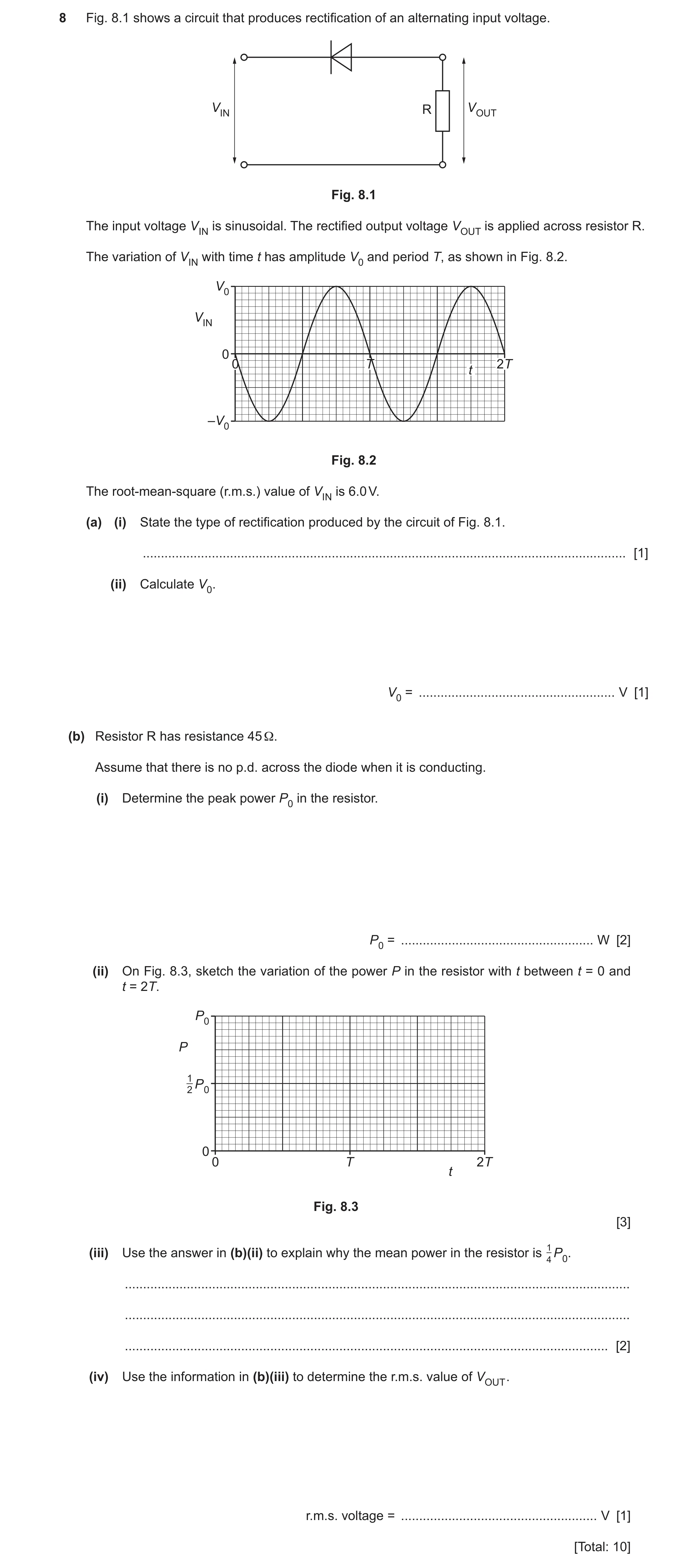
8 Fig. 8.1 shows a circuit that produces rectification of an alternating input voltage. VIN R VOUT Fig. 8.1 The input voltage VIN is sinusoidal. The rectified output voltage VOUT is applied across resistor R. The variation of VIN with time t has amplitude V0 and period T, as shown in Fig. 8.2. V0 VIN 0 0 T 2T t –V0 Fig. 8.2 The root-mean-square (r.m.s.) value of VIN is 6.0 V. (a) (i) State the type of rectification produced by the circuit of Fig. 8.1. … [1] (ii) Calculate V0. V0 = … V [1] (b) Resistor R has resistance 45 Ω. Assume that there is no p.d. across the diode when it is conducting. (i) Determine the peak power P0 in the resistor. P0 = … W [2] (ii) On Fig. 8.3, sketch the variation of the power P in the resistor with t between t = 0 and t = 2T. P0 P 1 2 P0 0 0 T 2T t Fig. 8.3 [3] (iii) Use the answer in (b)(ii) to explain why the mean power in the resistor is 14 P0. … … … [2] (iv) Use the information in (b)(iii) to determine the r.m.s. value of VOUT . r.m.s. voltage = … V [1] [Total: 10]
10 marks
Mark scheme: 8(a)(i) half-wave (rectification) B1 8(a)(ii) A1 V0 = 6.0 × 2 = 8.5 V 8(b)(i) P = V2 / R C1 P0 = 8.52 / 45 A1 = 1.6 W 8(b)(ii) two humps of width 0.5T and two sections of zero power of width 0.5T B1 all humps drawn have width 0.5T, minima at P = 0 and peaks at P = P0 B1 correct sinusoidal shape, with smooth troughs sitting on t-axis at P = 0 B1 8(b)(iii) 1 B1 mean power within each hump is P0 from the symmetry of the curve 2 additional half factor from removal of half of the power in each cycle B1 8(b)(iv) 〈P〉 = Vr.m.s.2 / R A1 Vr.m.s. = ( 1.6 / 4 ) 45 = 4.2 V
This question in 9702/42 May/June 2025
Q24 · A circuit that rectifies an alternating input voltage VIN and produces an output voltage… 9702/43 May/June 2025
6 Fig. 6.1 shows a circuit that rectifies an alternating input voltage VIN and produces an output voltage VOUT across a resistor R. W Y rectification VIN C R VOUT circuit X Z Fig. 6.1 The four terminals of the rectification circuit are labelled W, X, Y and Z. A capacitor C is connected in parallel with resistor R. (a) (i) State what is meant by rectification. … … [1] (ii) State the purpose of capacitor C. … … [1] (b) Fig. 6.2 shows the variations with time t of the potential differences (p.d.s) VIN and VOUT. 12 8 VOUT p.d. / V 4 0 0 10 20 30 40 t / ms –4 –8 VIN –12 Fig. 6.2 (i) The variation of VIN with t can be represented by VIN = A cos Bt where A and B are constants. Determine the values of A and B. Give a unit with your answer for A. A = … unit … B = … rad s–1 [2] (ii) Determine the type of rectification produced by the circuit in Fig. 6.1. … [1] (iii) On Fig. 6.3, draw the circuit diagram for the components inside the rectification circuit. W Y X Z Fig. 6.3 [2] (iv) Determine a value for the time constant for the discharge of the capacitor C through the resistor R in Fig. 6.1. time constant = … s [3] (c) The capacitor C has a capacitance of 570 μF. Use your answer in (b)(iv) to determine the resistance of resistor R. resistance = … Ω [2] [Total: 12]
12 marks
Mark scheme: 6(a)(i) conversion from a.c. to d.c. B1 6(a)(ii) smoothing B1 6(b)(i) A = 12 V A1 B = 2 / (20 × 10–3) A1 = 310 rad s–1 6(b)(ii) full-wave (rectification) B1 6(b)(iii) four diodes shown, with correct circuit symbols B1 four diodes correctly connected to form a bridge rectifier B1 6(b)(iv) V = V0 exp (–t / ) C1 or V = V0 exp (–t / RC) and = RC 8.0 = 12 exp (– 7.3 × 10⁻³ / ) C1 = 0.018 s A1 6(c) time constant = RC C1 R = (0.018 / 570 × 10–6) A1 = 32
This question in 9702/43 May/June 2025
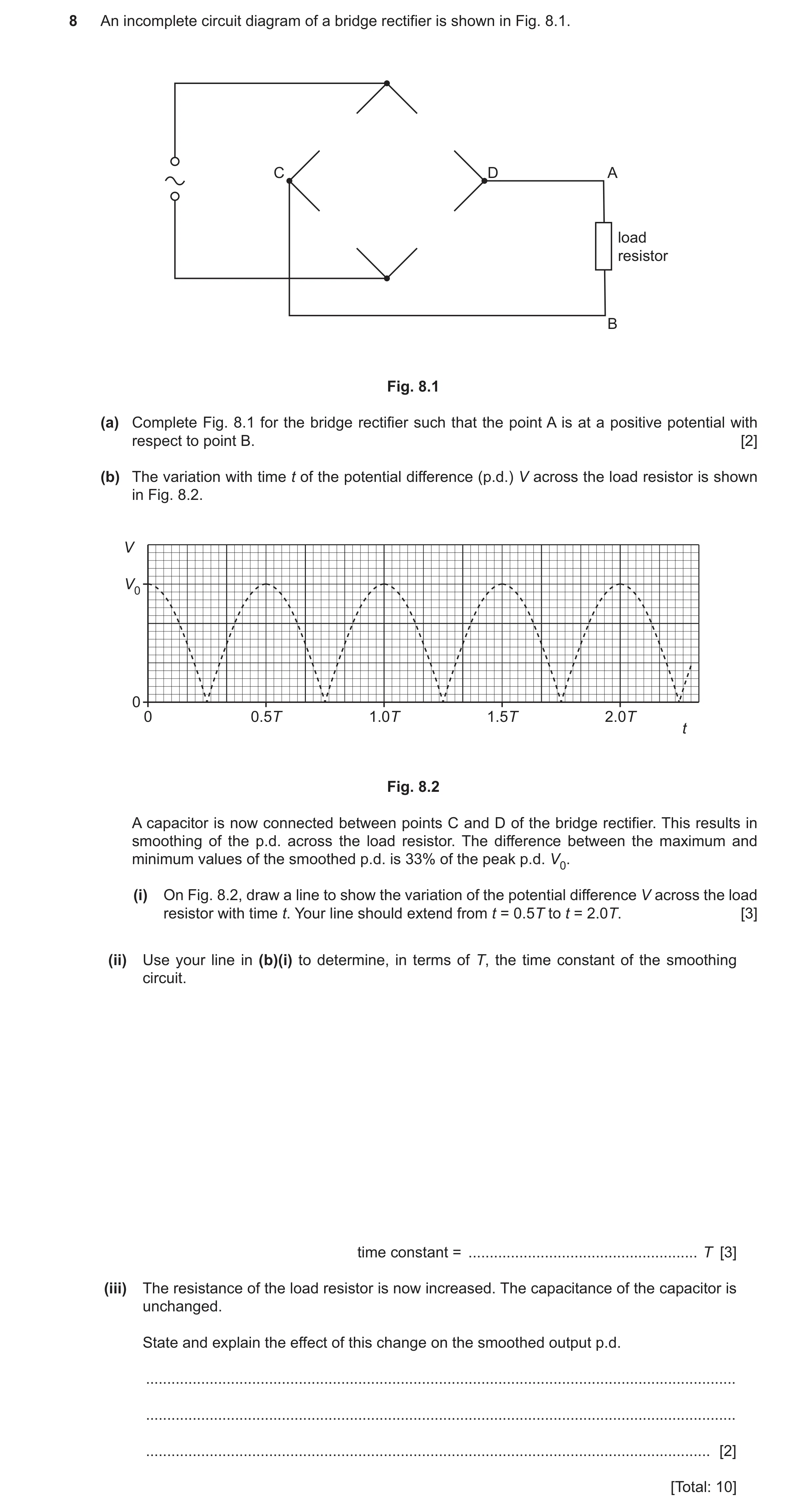
Q25 · An incomplete circuit diagram of a bridge rectifier is shown in Fig 9702/44 May/June 2025
8 An incomplete circuit diagram of a bridge rectifier is shown in Fig. 8.1. C D A load resistor B Fig. 8.1 (a) Complete Fig. 8.1 for the bridge rectifier such that the point A is at a positive potential with respect to point B. [2] (b) The variation with time t of the potential difference (p.d.) V across the load resistor is shown in Fig. 8.2. V V0 0 0 0.5T 1.0T 1.5T 2.0T t Fig. 8.2 A capacitor is now connected between points C and D of the bridge rectifier. This results in smoothing of the p.d. across the load resistor. The difference between the maximum and minimum values of the smoothed p.d. is 33% of the peak p.d. V0. (i) On Fig. 8.2, draw a line to show the variation of the potential difference V across the load resistor with time t. Your line should extend from t = 0.5T to t = 2.0T. [3] (ii) Use your line in (b)(i) to determine, in terms of T, the time constant of the smoothing circuit. time constant = … T [3] (iii) The resistance of the load resistor is now increased. The capacitance of the capacitor is unchanged. State and explain the effect of this change on the smoothed output p.d. … … … [2] [Total: 10]
10 marks
Mark scheme: 8(a) four diodes shown (one in each gap) with correct circuit symbols B1 all four diodes connected in correct direction (pointing left to right) B1 8(b)(i) three lines showing exponential decay from the peaks at 0.5T, 1.0T and 1.5T, ending at the point where the decay meets B1 the next rising peak three curved lines rising along the upwards dotted lines from the minima to the peaks at 1.0T, 1.5T and 2.0T B1 minimum V at (2 / 3) V0 B1 8(b)(ii) from graph: discharge time (from V0 to (2 / 3)V0) = (11 / 30) T C1 (2 / 3) V0 = V0 exp (– (11 / 30)T / τ) C1 ln (2 / 3) = – 11T / 30τ A1 τ = 0.90 T 8(b)(iii) time constant is increased B1 line shows a larger minimum voltage B1 or smaller difference between maximum and minimum voltages
This question in 9702/44 May/June 2025
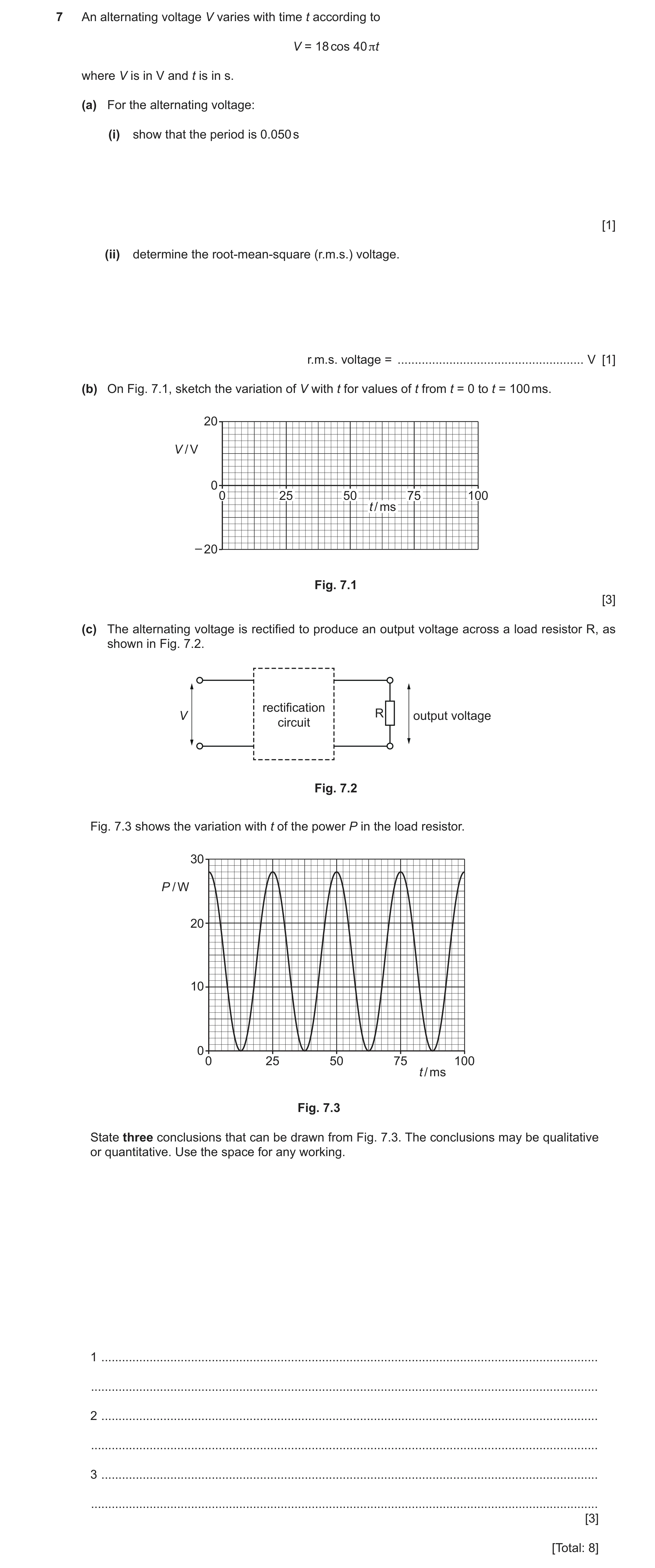
Q26 · An alternating voltage V varies with time t according to V = 18 cos 40 πt where V is in V… 9702/42 Oct/Nov 2025
7 An alternating voltage V varies with time t according to V = 18 cos 40 πt where V is in V and t is in s. (a) For the alternating voltage: (i) show that the period is 0.050 s [1] (ii) determine the root-mean-square (r.m.s.) voltage. r.m.s. voltage = … V [1] (b) On Fig. 7.1, sketch the variation of V with t for values of t from t = 0 to t = 100 ms. 20 V / V 0 0 25 50 75 100 t / ms – 20 Fig. 7.1 [3] (c) The alternating voltage is rectified to produce an output voltage across a load resistor R, as shown in Fig. 7.2. rectification V R output voltage circuit Fig. 7.2 Fig. 7.3 shows the variation with t of the power P in the load resistor. 30 P / W 20 10 0 0 25 50 75 100 t / ms Fig. 7.3 State three conclusions that can be drawn from Fig. 7.3. The conclusions may be qualitative or quantitative. Use the space for any working. 1 … … 2 … … 3 … … [3] [Total: 8]
8 marks
Mark scheme: 7(a)(i) T = 2 / 40 = 0.050 s A1 7(a)(ii) Vr.m.s. = 18 / √2 A1 = 13 V 7(b) sinusoidal curve of period 50 ms from t = 0 to t = 100 ms B1 correct phase (VMAX at t = 0, 50, 100 ms and –VMAX at 25, 75 ms etc.) B1 maximum and minimum voltages shown as 18 V B1 7(c) Any three points from: B3 • rectification is full-wave • mean power = 14 W • resistance of R = 12 • peak current in R = 1.6 A or r.m.s. current in R = 1.1 A • period of output voltage / power = 25 ms or frequency of output voltage / power = 40 Hz or angular frequency of output voltage / power = 250 rad s–1
This question in 9702/42 Oct/Nov 2025
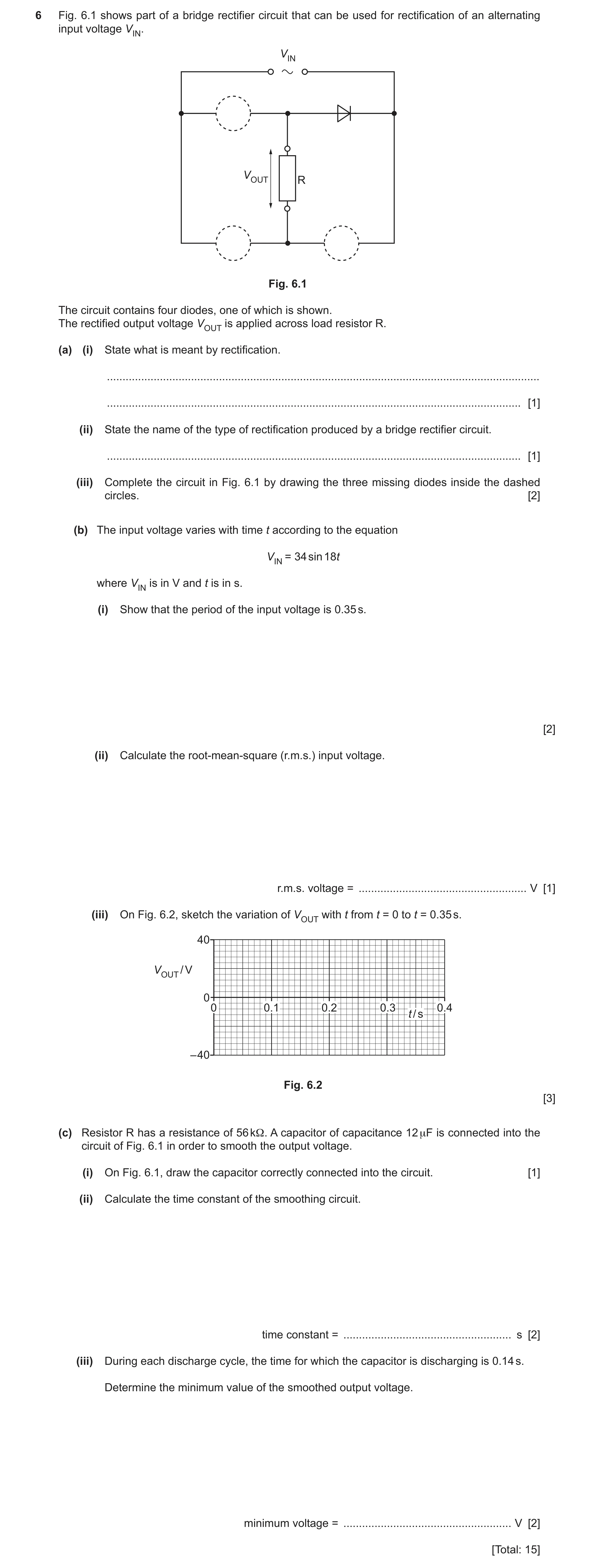
Q27 · Part of a bridge rectifier circuit that can be used for rectification of an alternating… 9702/44 Oct/Nov 2025
6 Fig. 6.1 shows part of a bridge rectifier circuit that can be used for rectification of an alternating input voltage VIN. VIN VOUT R Fig. 6.1 The circuit contains four diodes, one of which is shown. The rectified output voltage VOUT is applied across load resistor R. (a) (i) State what is meant by rectification. … … [1] (ii) State the name of the type of rectification produced by a bridge rectifier circuit. … [1] (iii) Complete the circuit in Fig. 6.1 by drawing the three missing diodes inside the dashed circles. [2] (b) The input voltage varies with time t according to the equation VIN = 34 sin 18t where VIN is in V and t is in s. (i) Show that the period of the input voltage is 0.35 s. [2] (ii) Calculate the root-mean-square (r.m.s.) input voltage. r.m.s. voltage = … V [1] (iii) On Fig. 6.2, sketch the variation of VOUT with t from t = 0 to t = 0.35 s. 40 VOUT / V 0 0 0.1 0.2 0.3 0.4 t / s – 40 Fig. 6.2 [3] (c) Resistor R has a resistance of 56 kΩ. A capacitor of capacitance 12 μF is connected into the circuit of Fig. 6.1 in order to smooth the output voltage. (i) On Fig. 6.1, draw the capacitor correctly connected into the circuit. [1] (ii) Calculate the time constant of the smoothing circuit. time constant = … s [2] (iii) During each discharge cycle, the time for which the capacitor is discharging is 0.14 s. Determine the minimum value of the smoothed output voltage. minimum voltage = … V [2] [Total: 15]
15 marks
Mark scheme: 6(a)(i) conversion of a.c. to d.c. B1 6(a)(ii) full-wave (rectification) B1 6(a)(iii) three diodes with correct symbols connected into the circuit B1 lower-left diode shown pointing towards the right and upper-left and lower-right diodes both shown pointing towards the left B1 6(b)(i) = 18 (rad s–1) C1 T = 2 / 18 = 0.35 s A1 6(b)(ii) Vr.m.s.= 34 / √2 A1 = 24 V 6(b)(iii) sinusoidal ‘humps’ with minimum VOUT = 0 and non-zero VOUT all same sign B1 peak VOUT shown as 34 V or –34 V B1 two ‘humps’ shown, with VOUT always with same sign and VOUT = 0 at t = 0, t = 0.175 s and t = 0.350 s and non-zero in B1 between 6(c)(i) correct circuit symbol for capacitor, connected in parallel with resistor B1 6(c)(ii) time constant = RC C1 = 56 103 12 10–6 A1 = 0.67 s 6(c)(iii) Vmin = 34 exp (–0.14 / 0.67) C1 = 28 V A1
This question in 9702/44 Oct/Nov 2025
 6 / 46
 7 / 46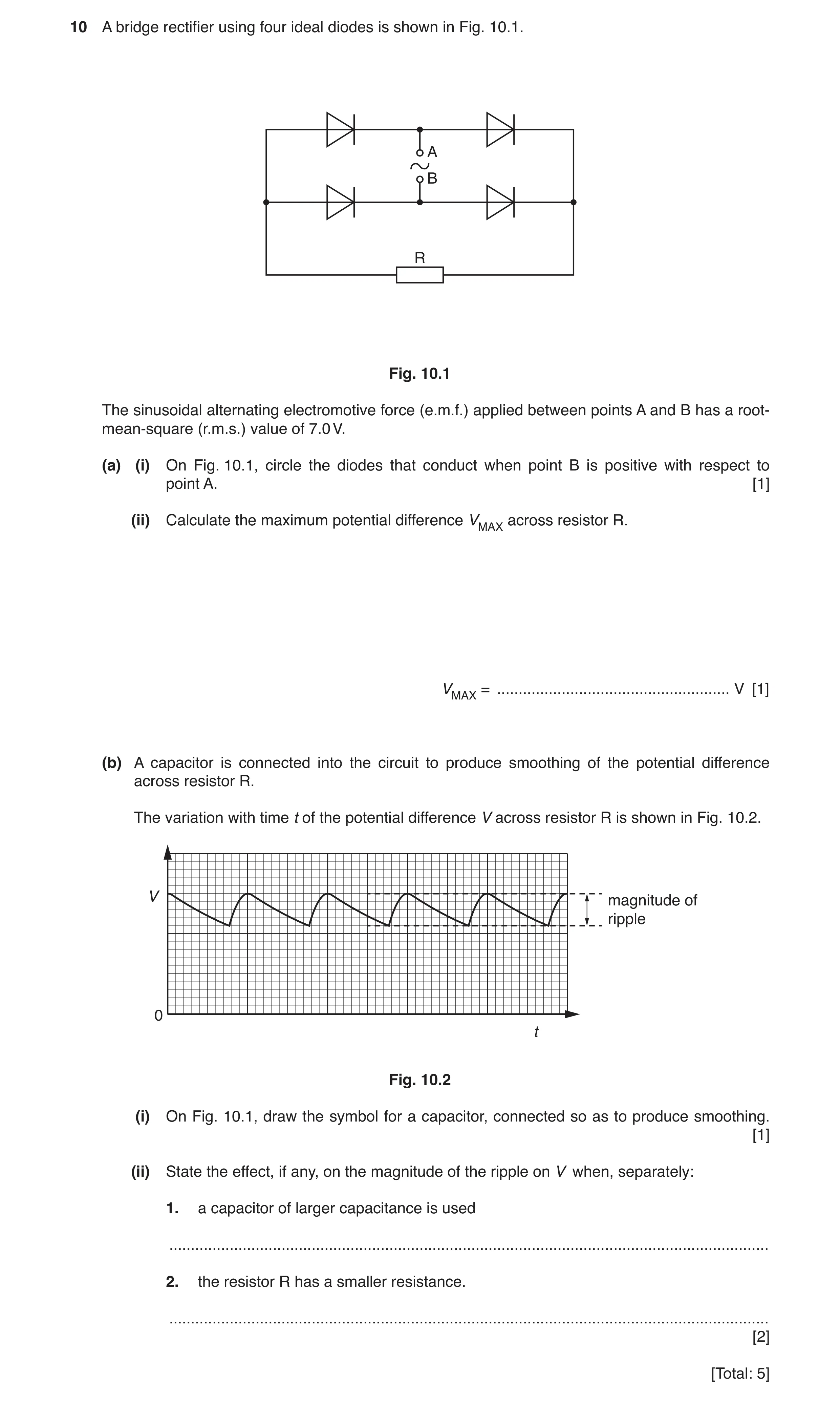
 10
10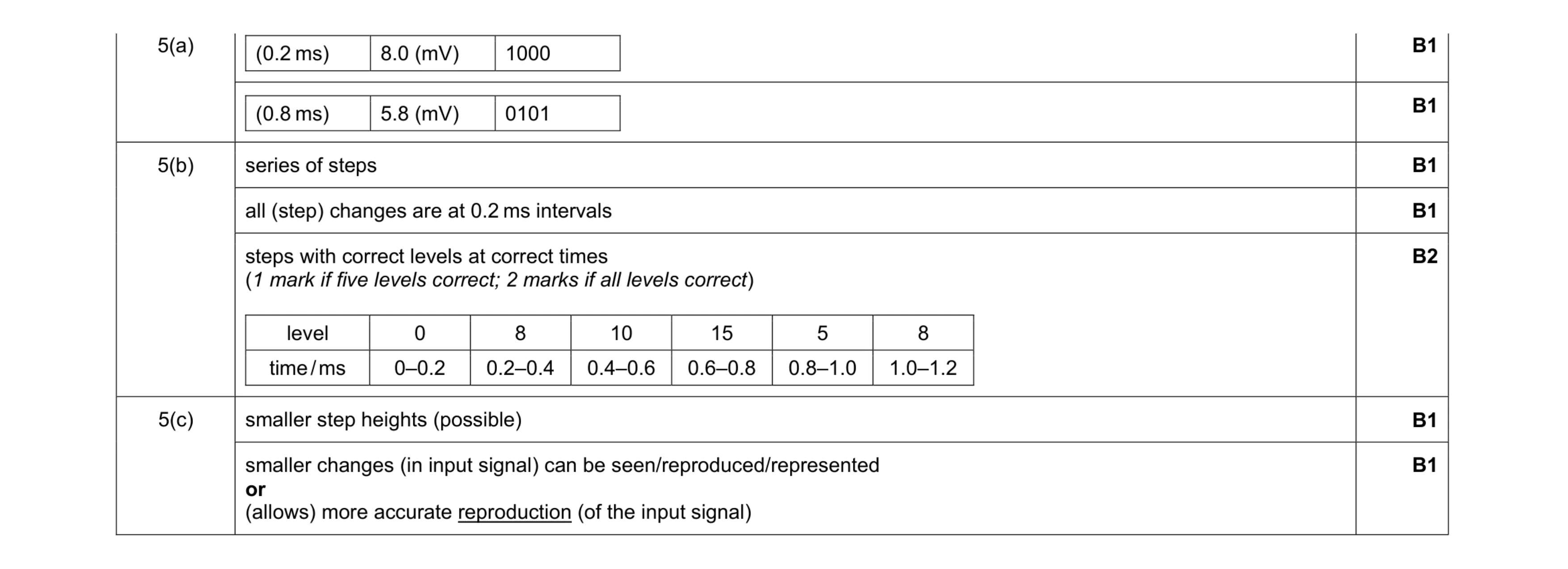 8
8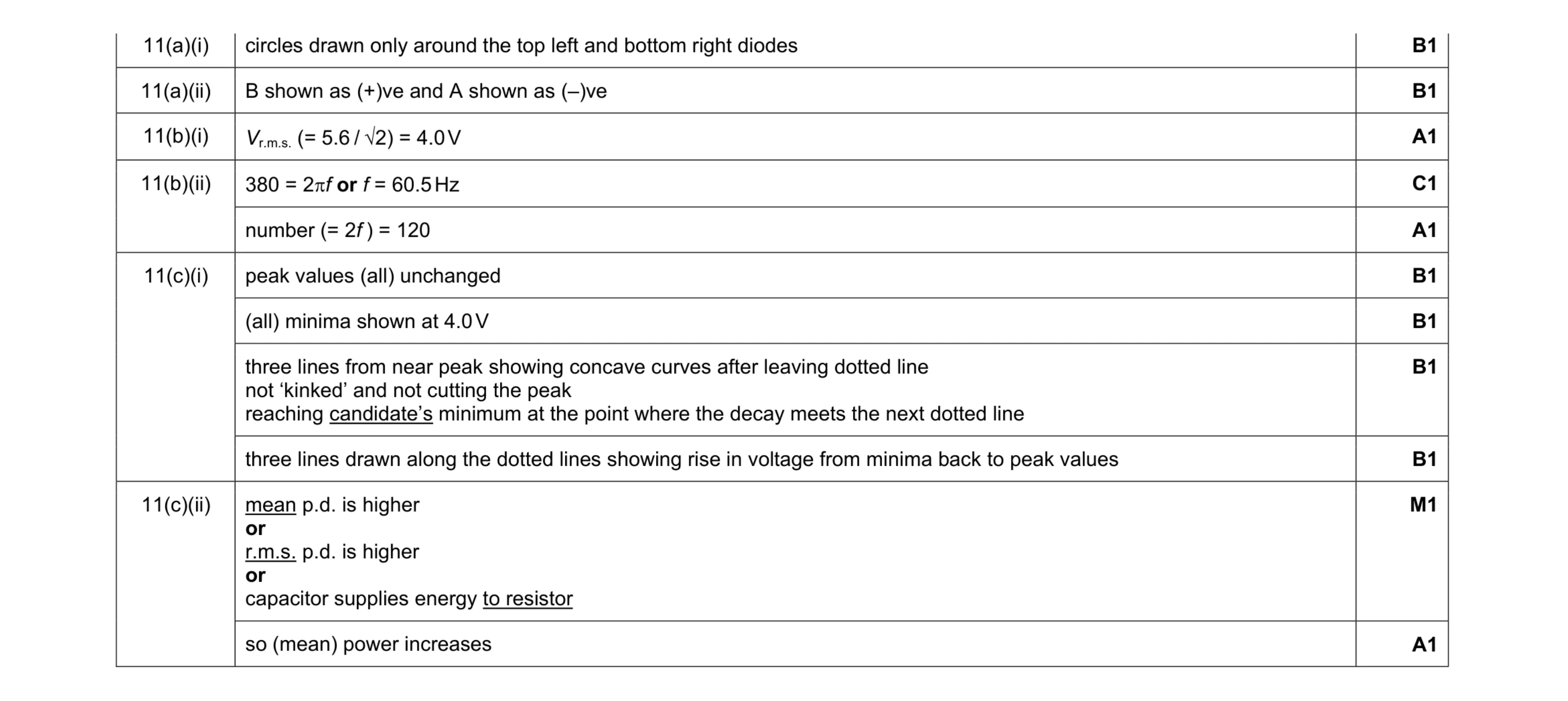 11
11 4
4 4
4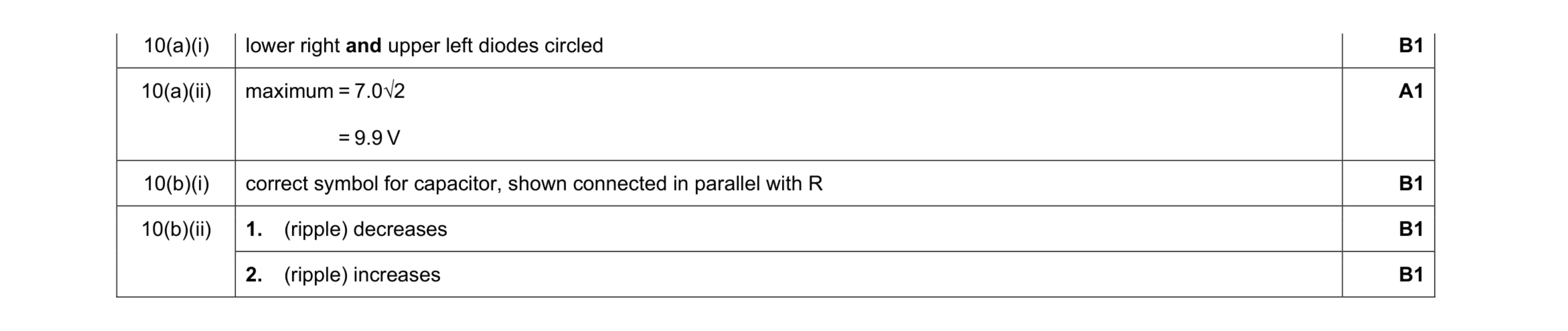 5
5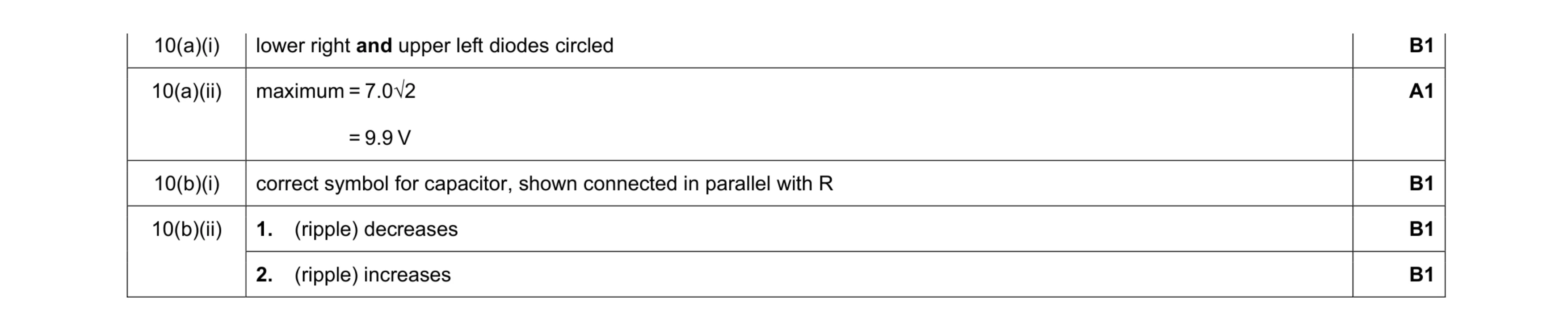 5
5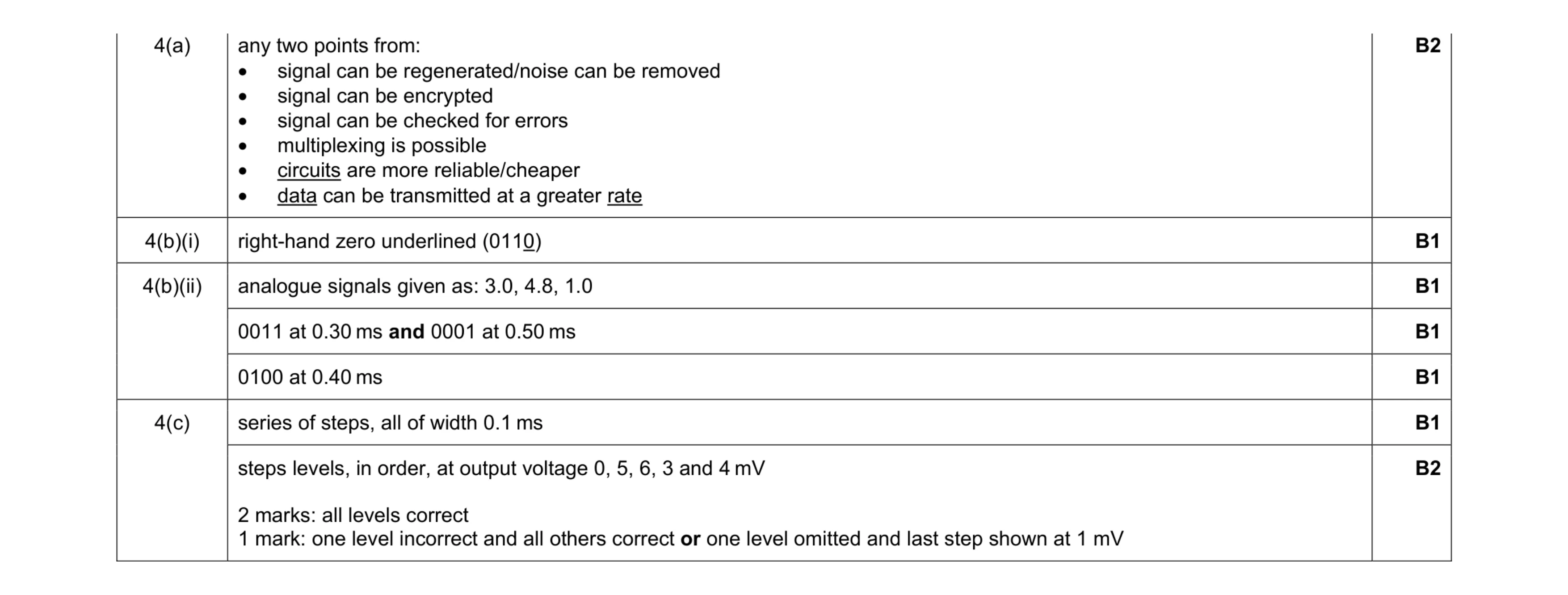 9
9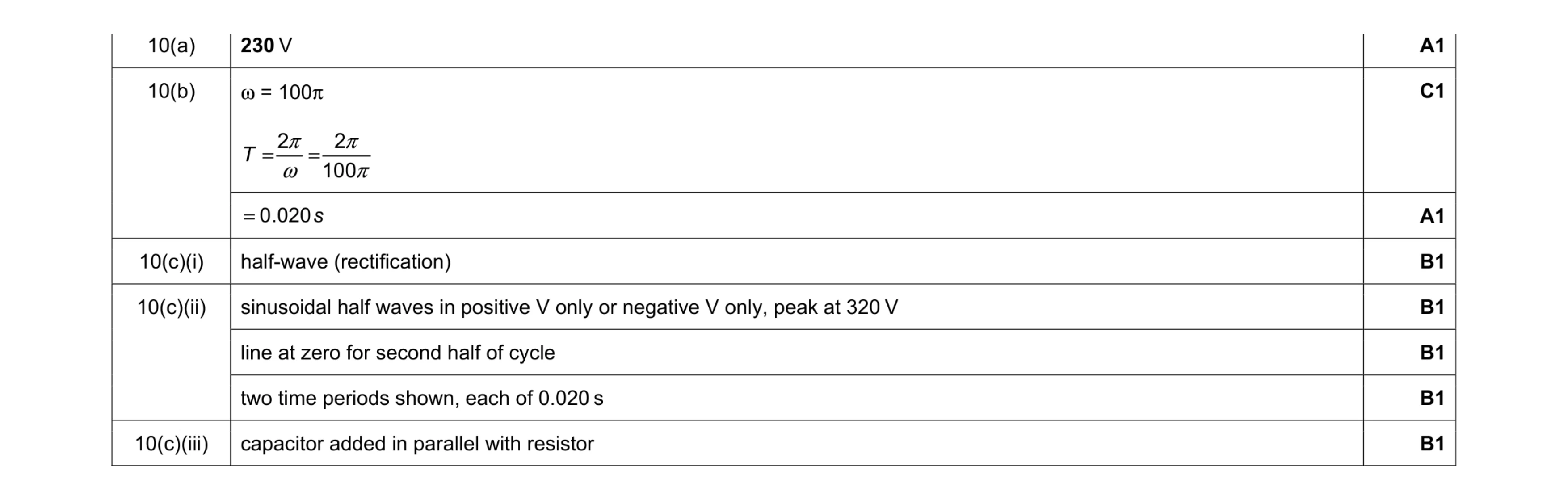 8
8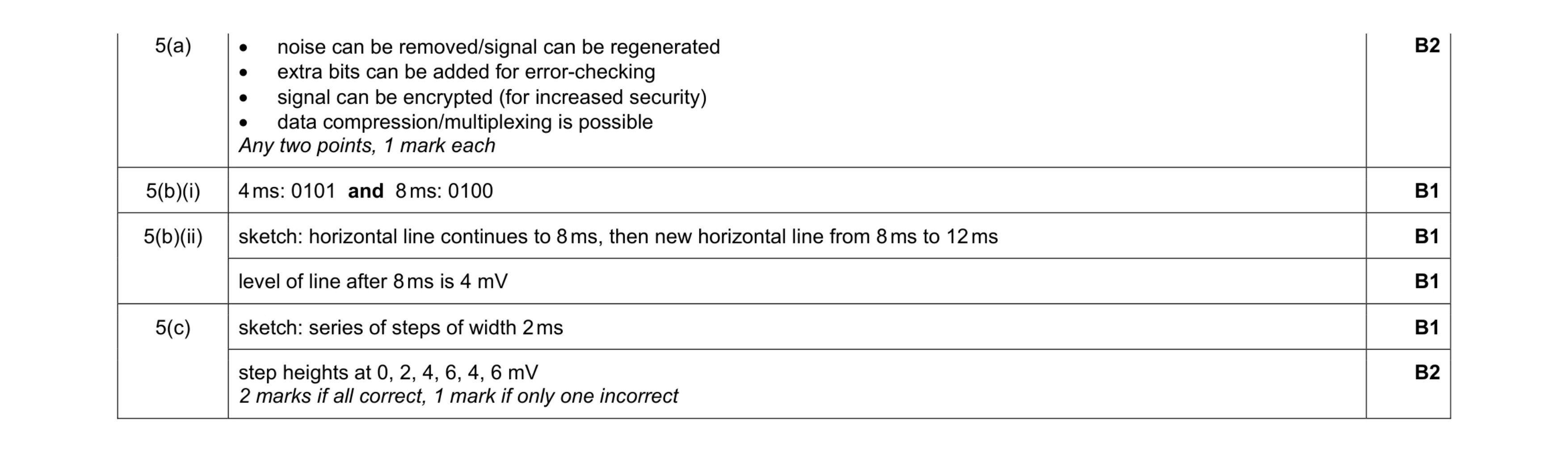 8
8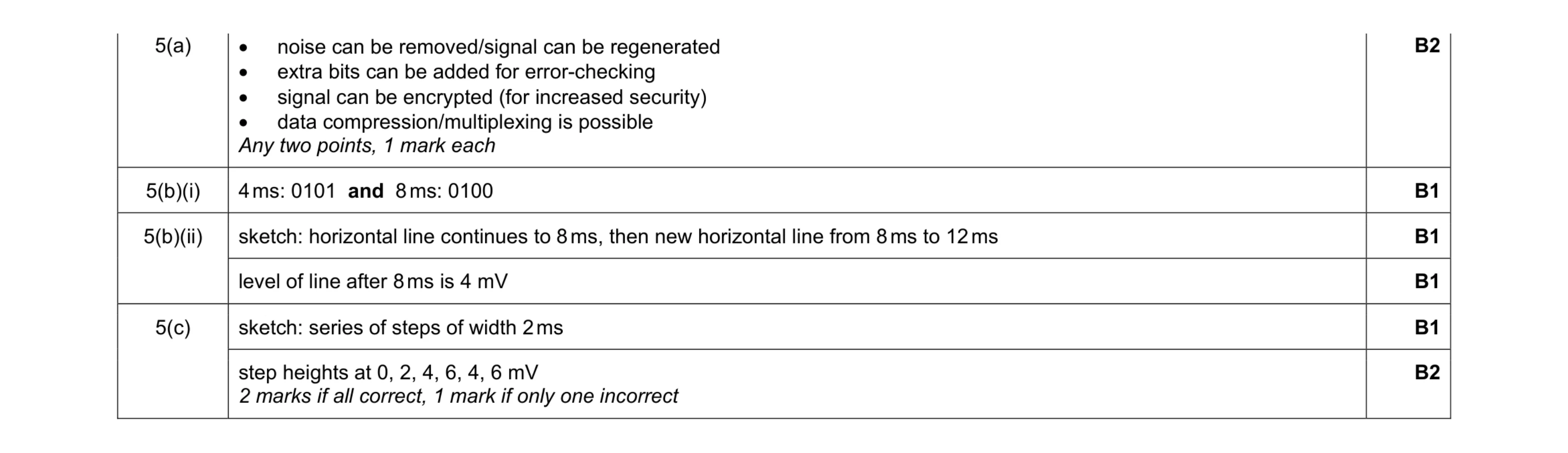 8
8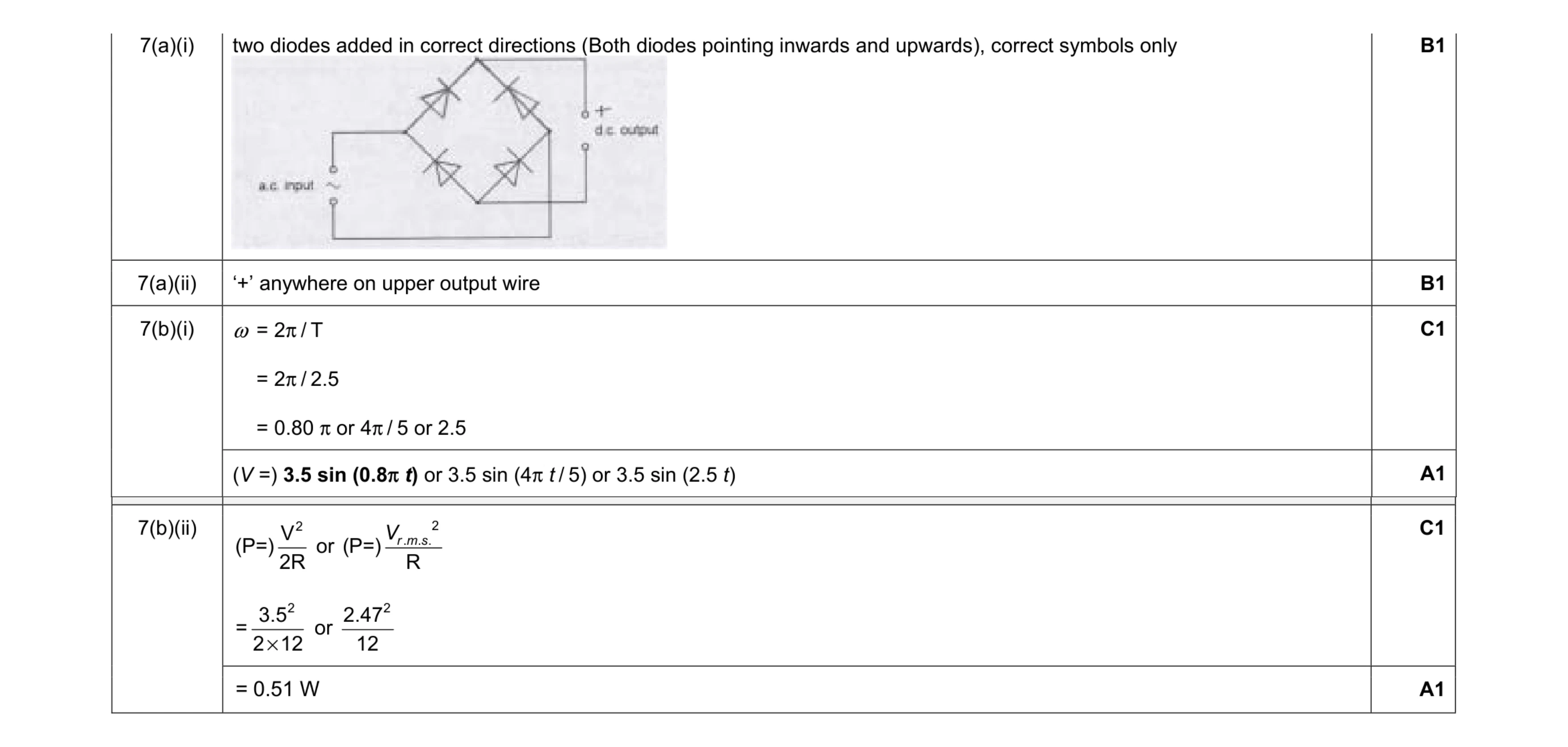 6
6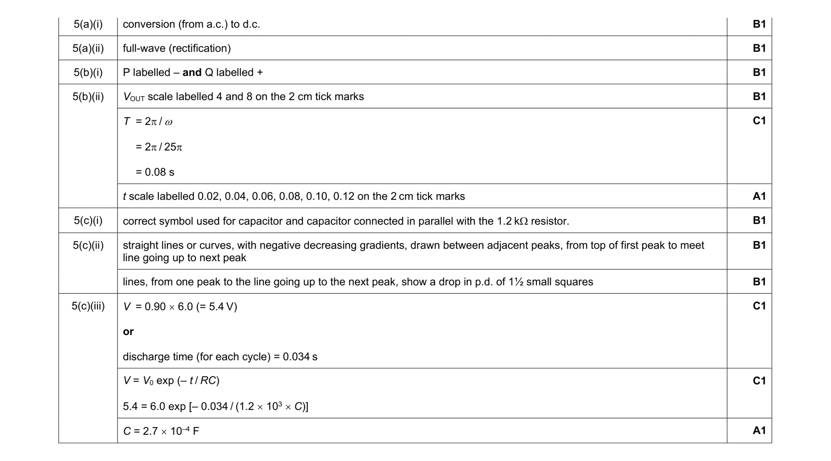 12
12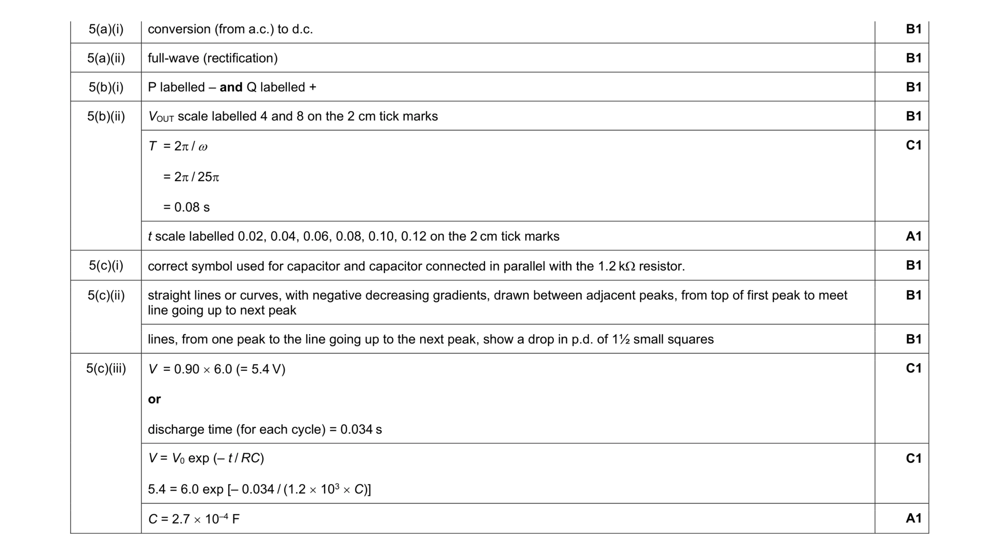 12
12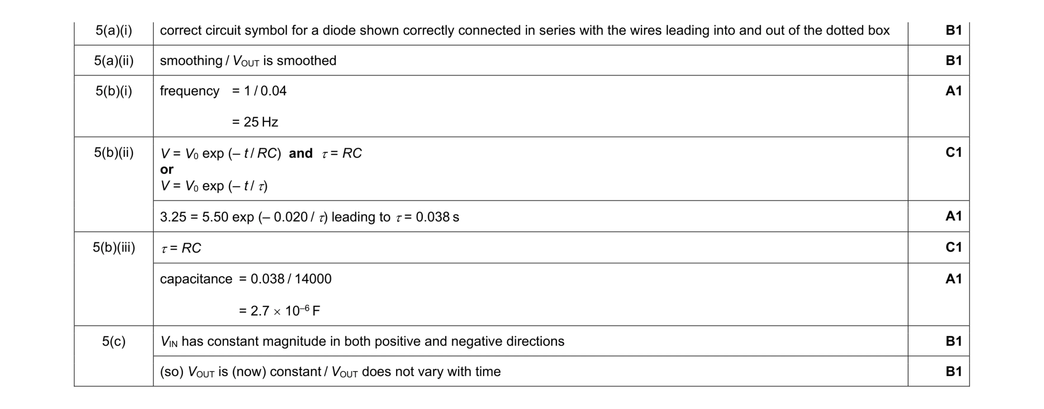 9
9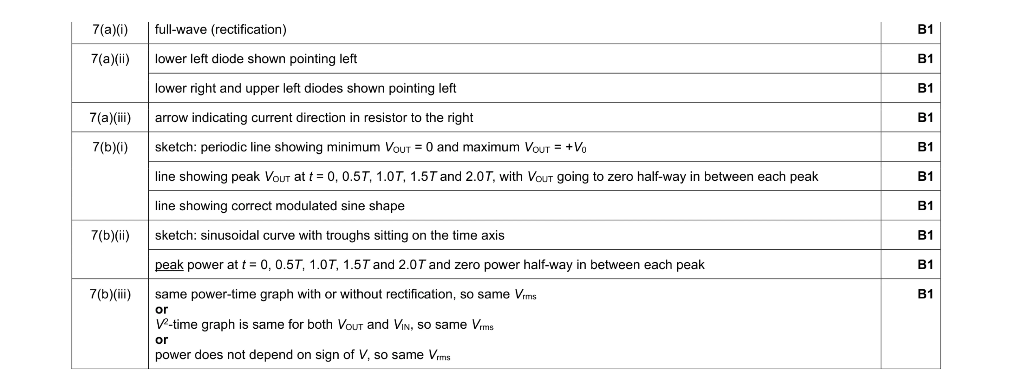 10
10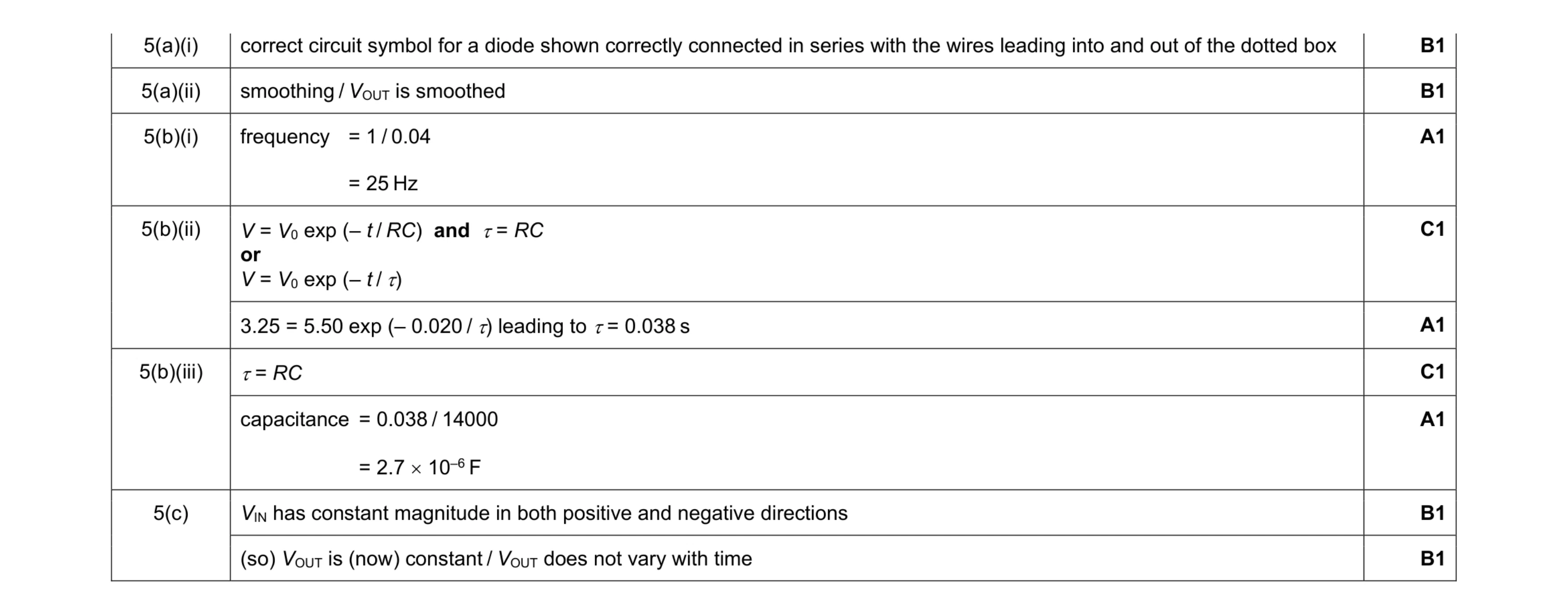 9
9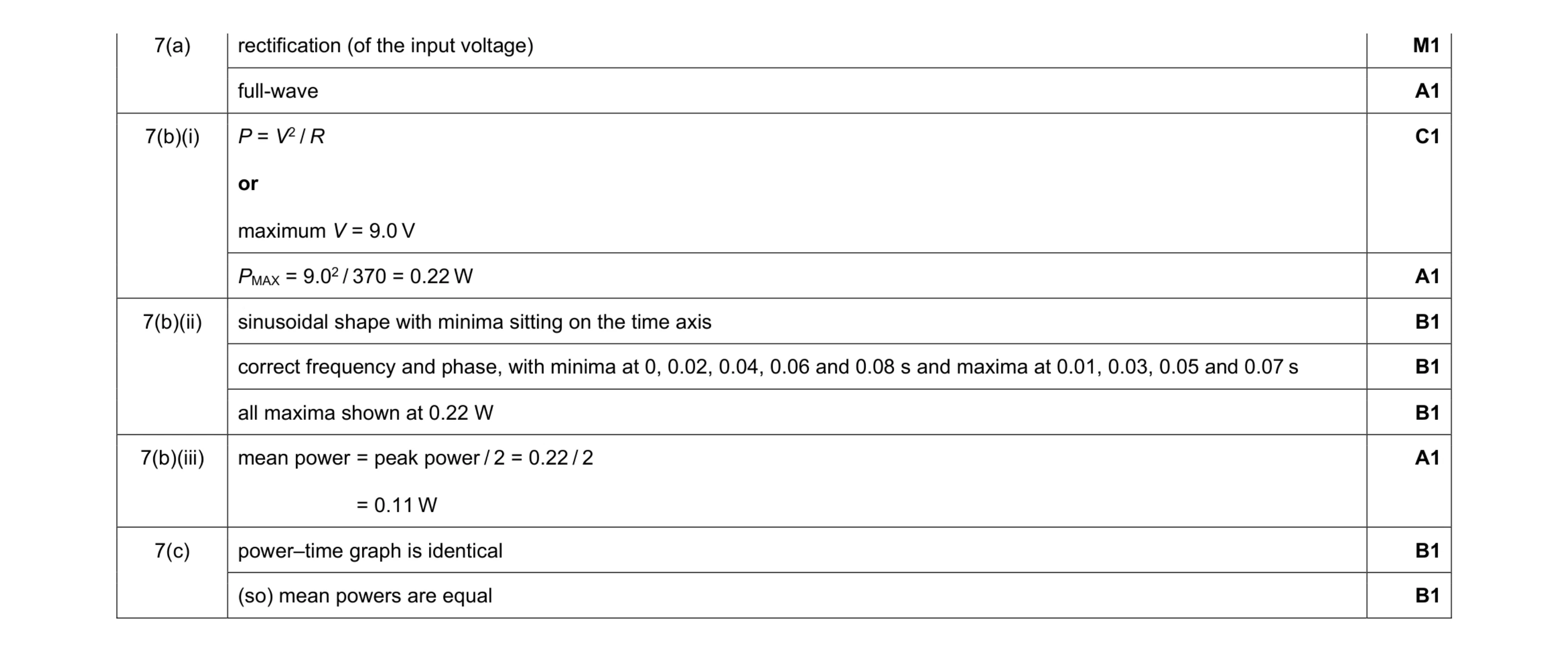 10
10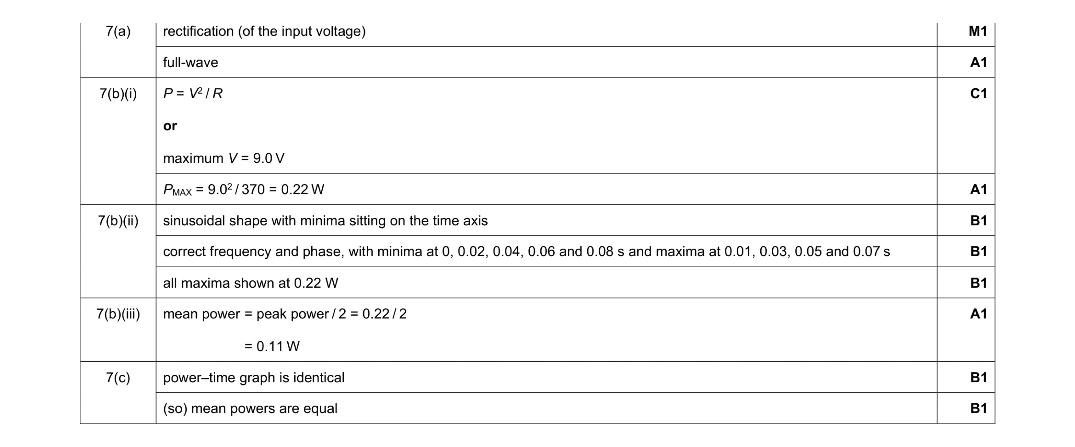 10
10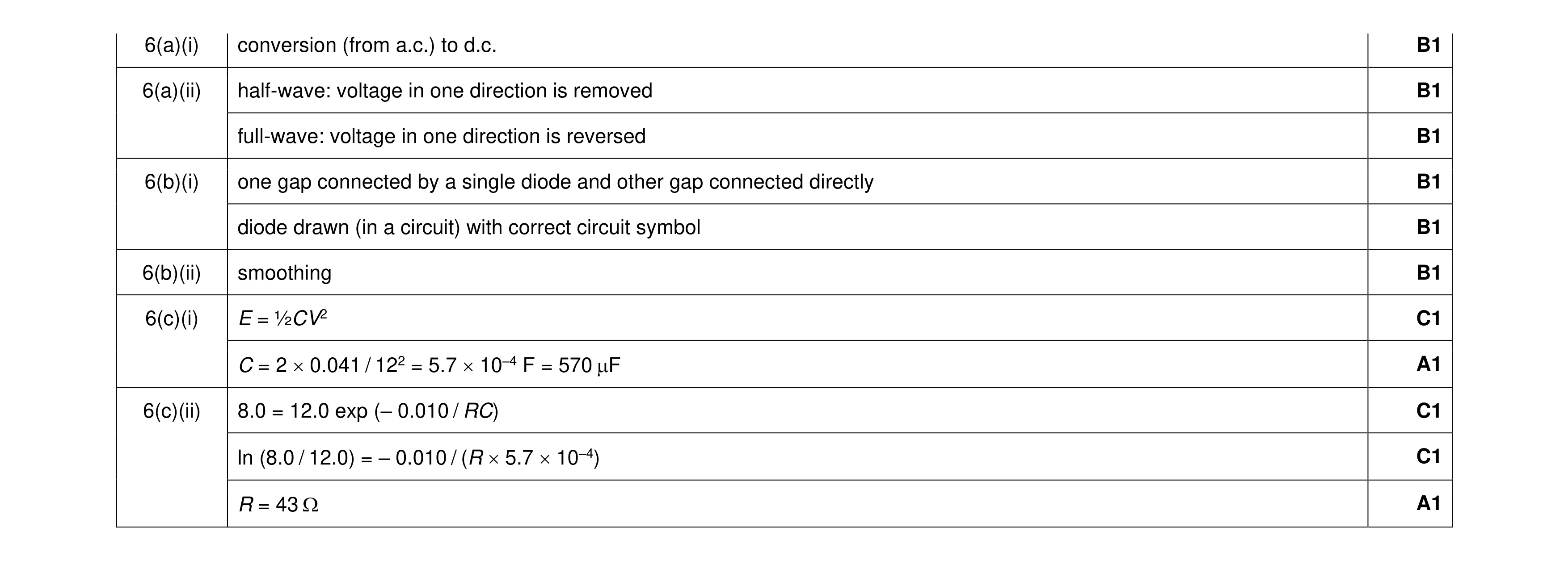 11
11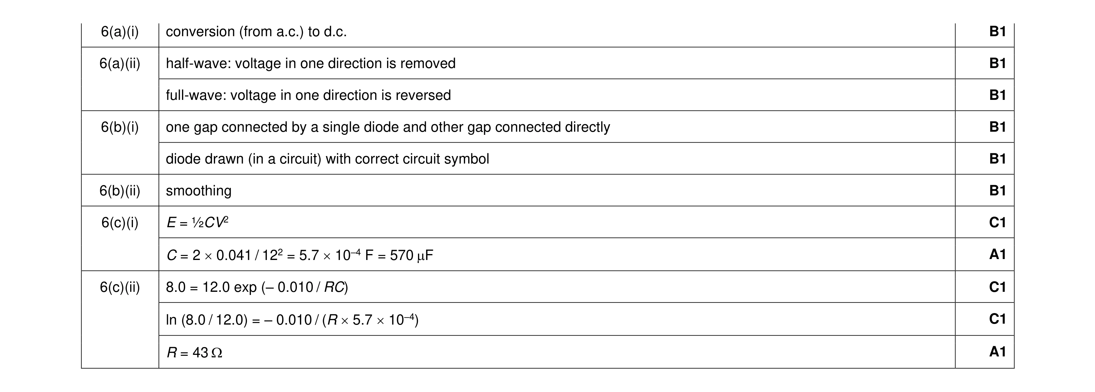 11
11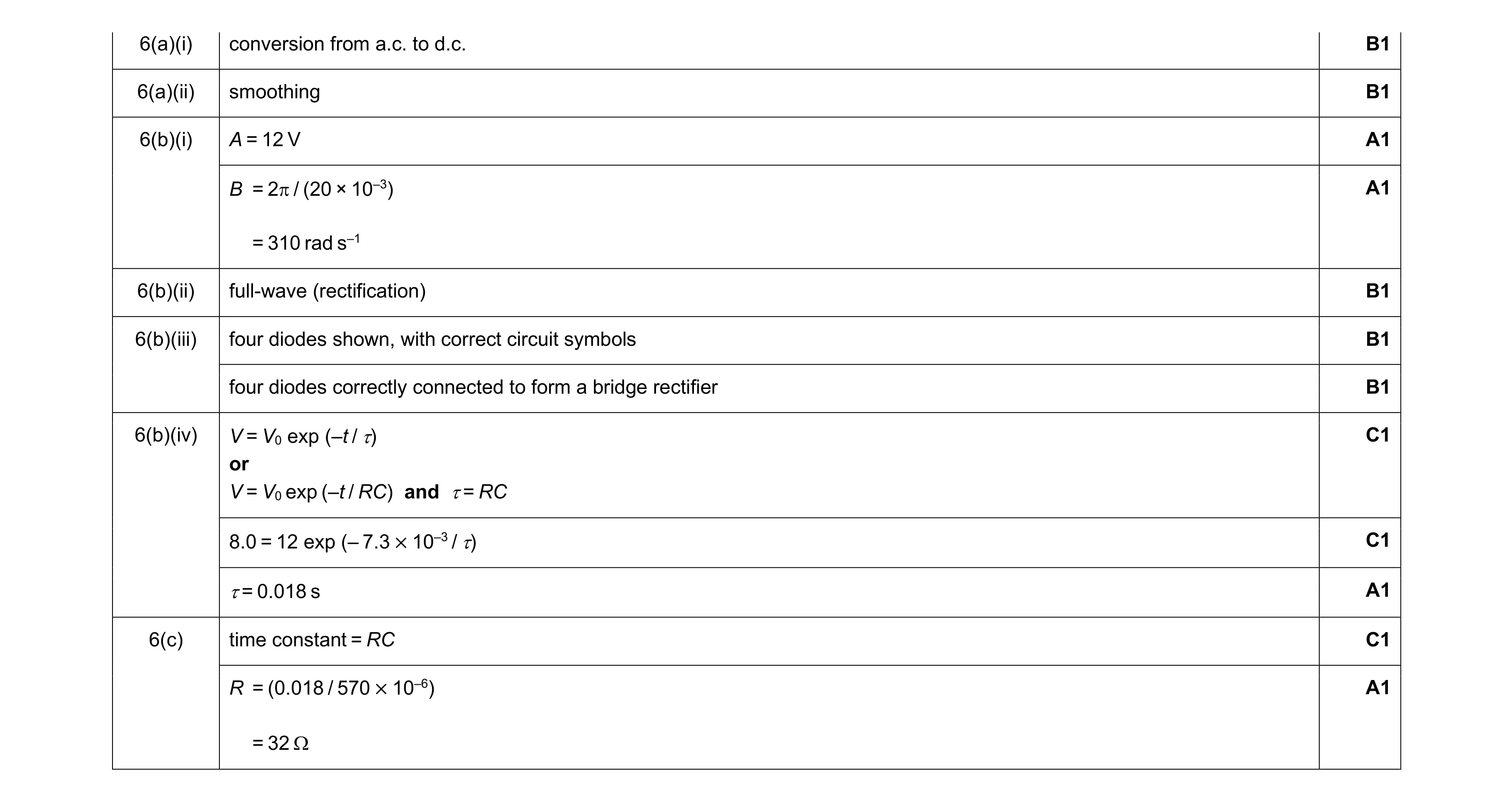 12
12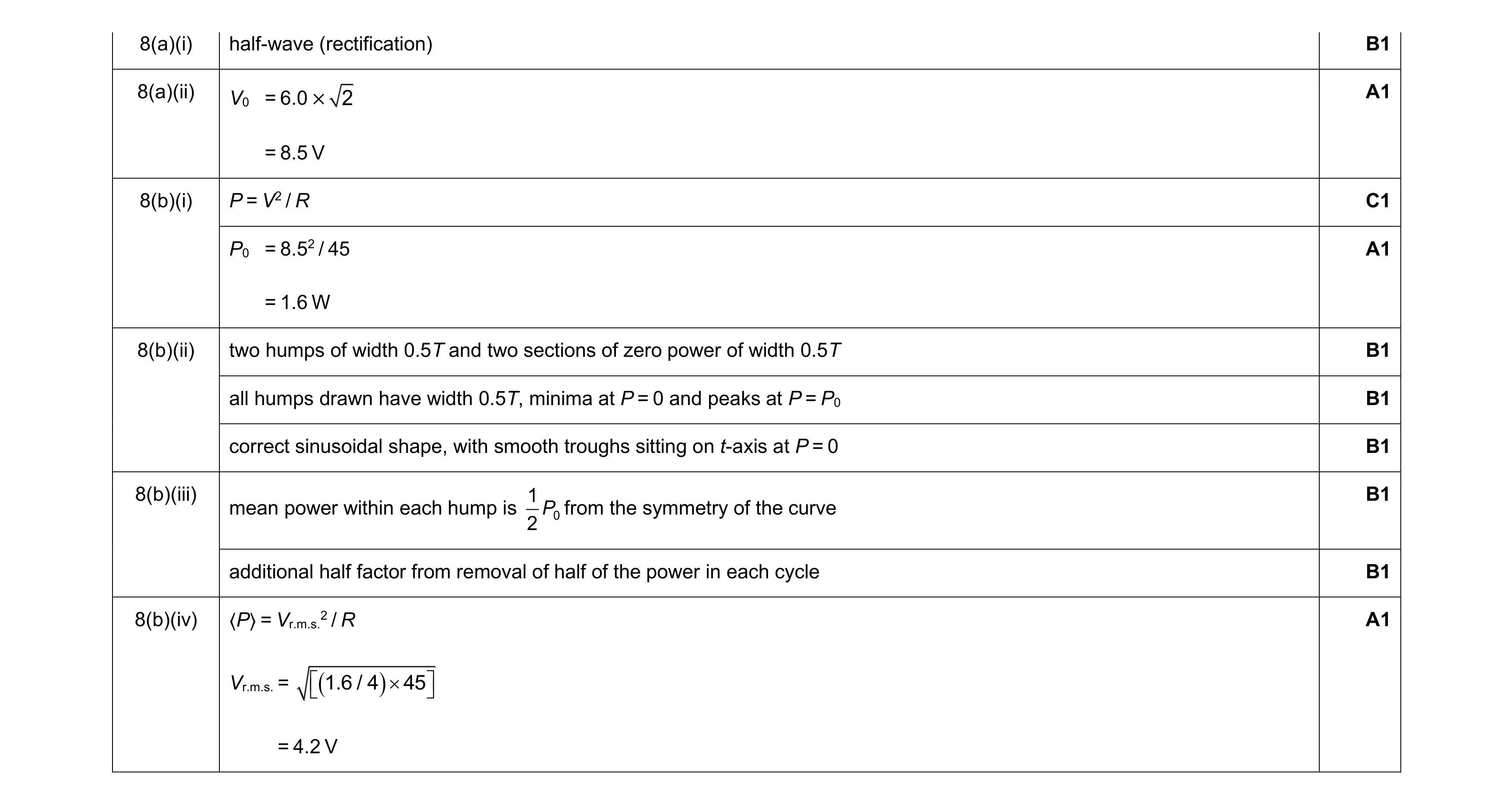 10
10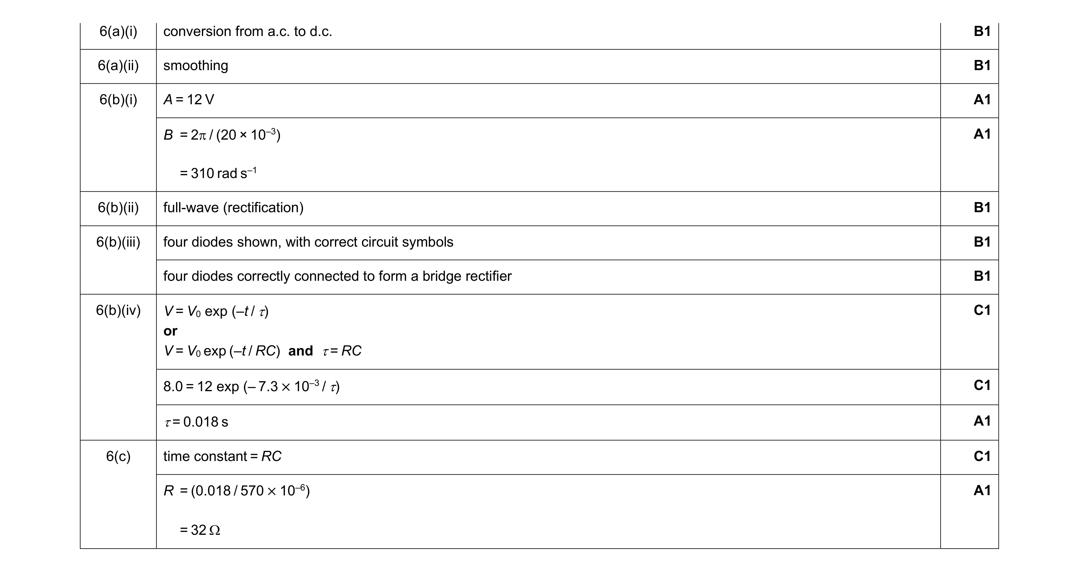 12
12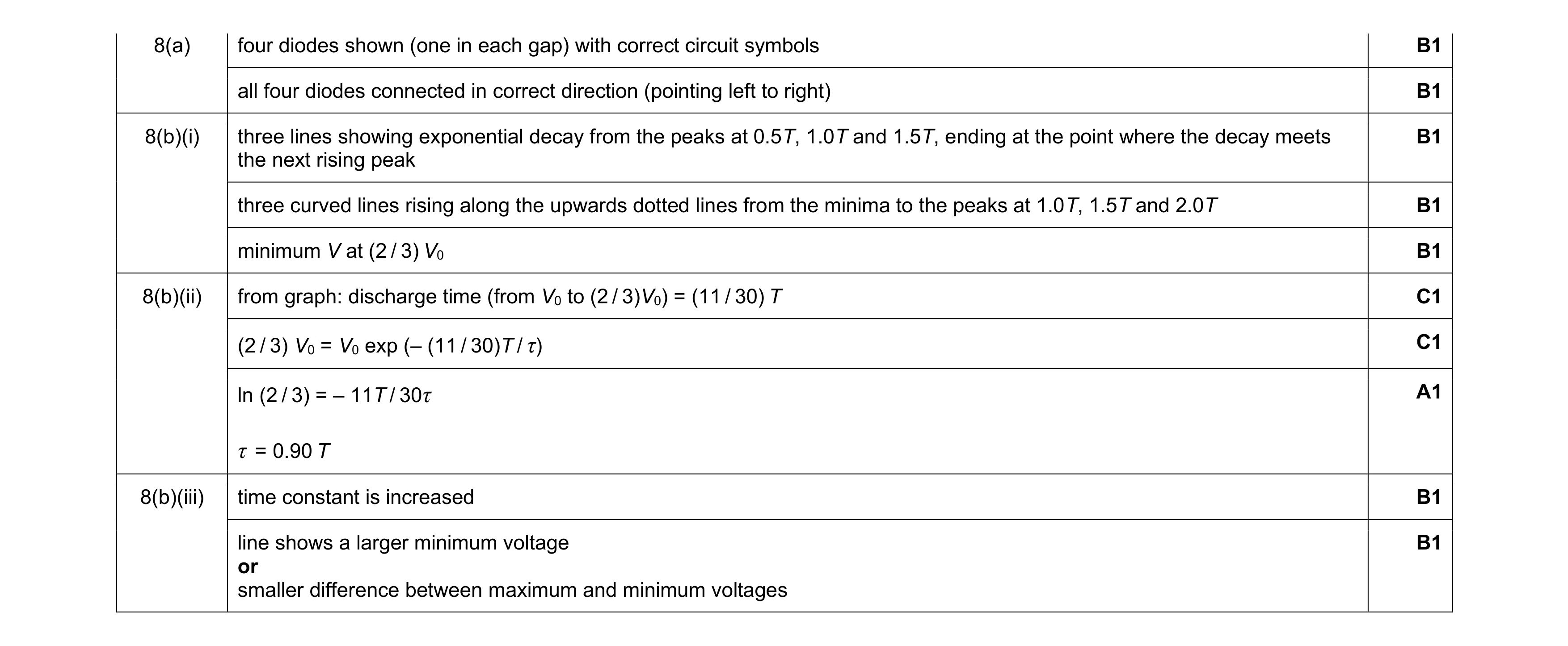 10
10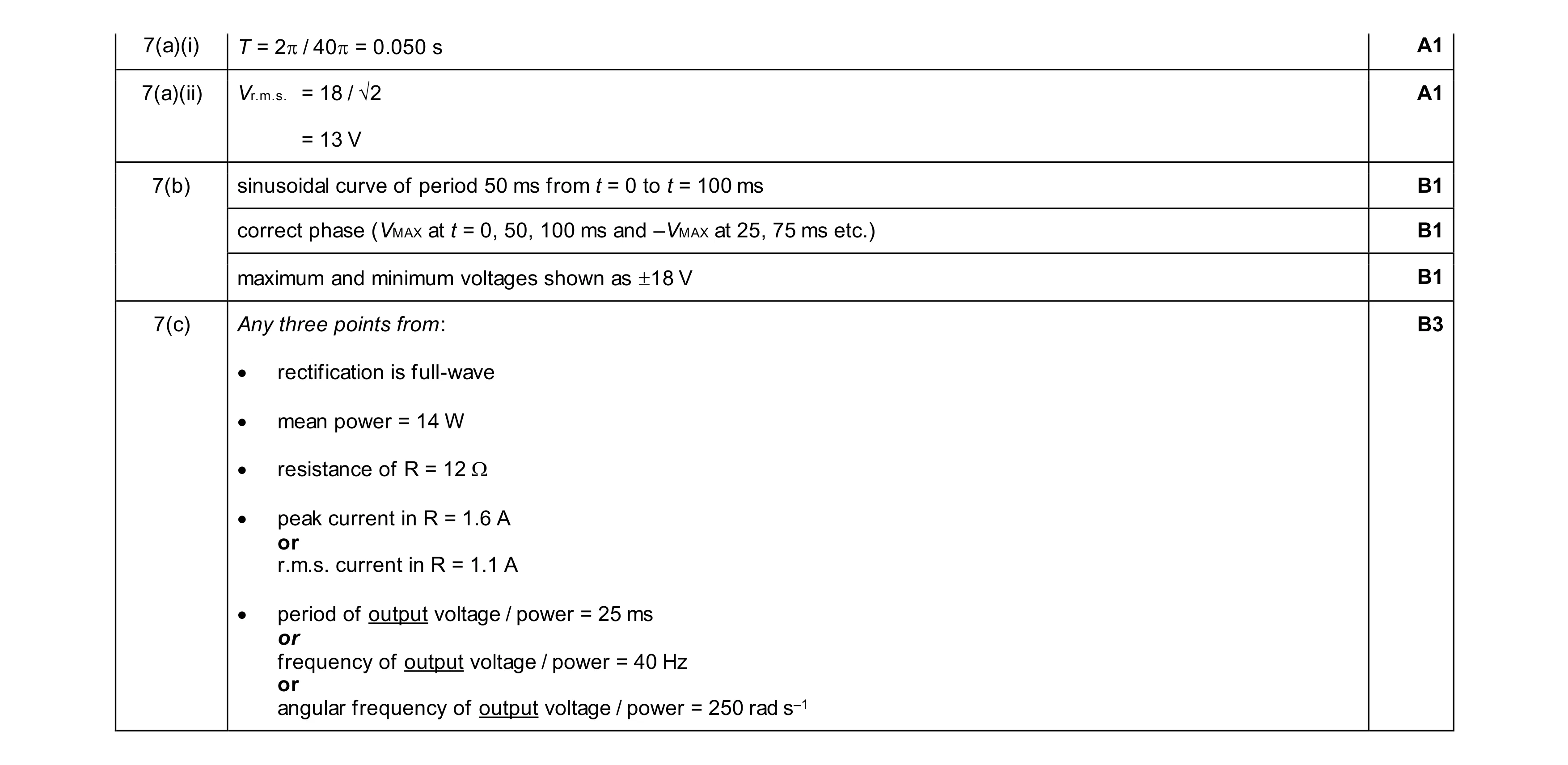 8
8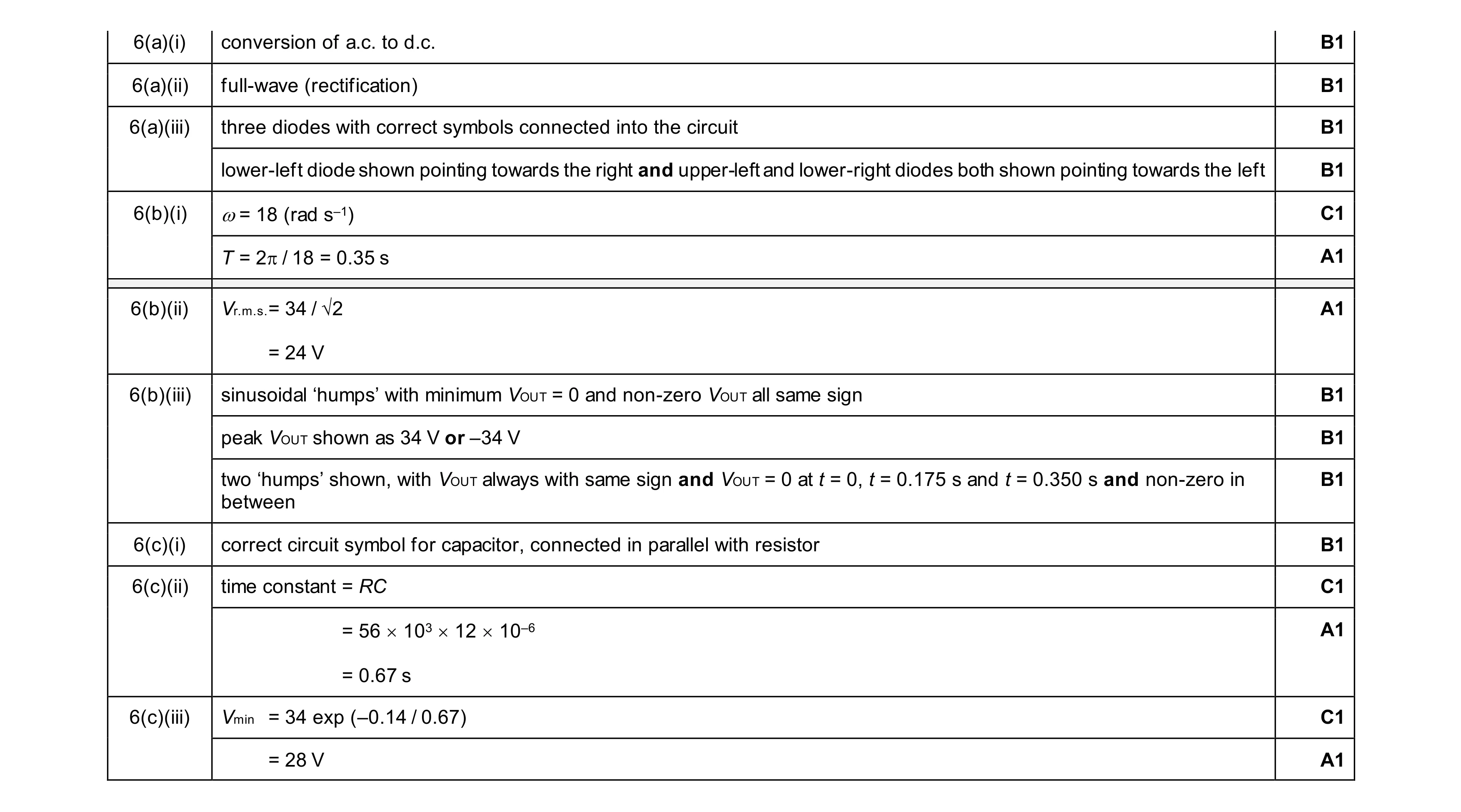 15
15