Questions as text
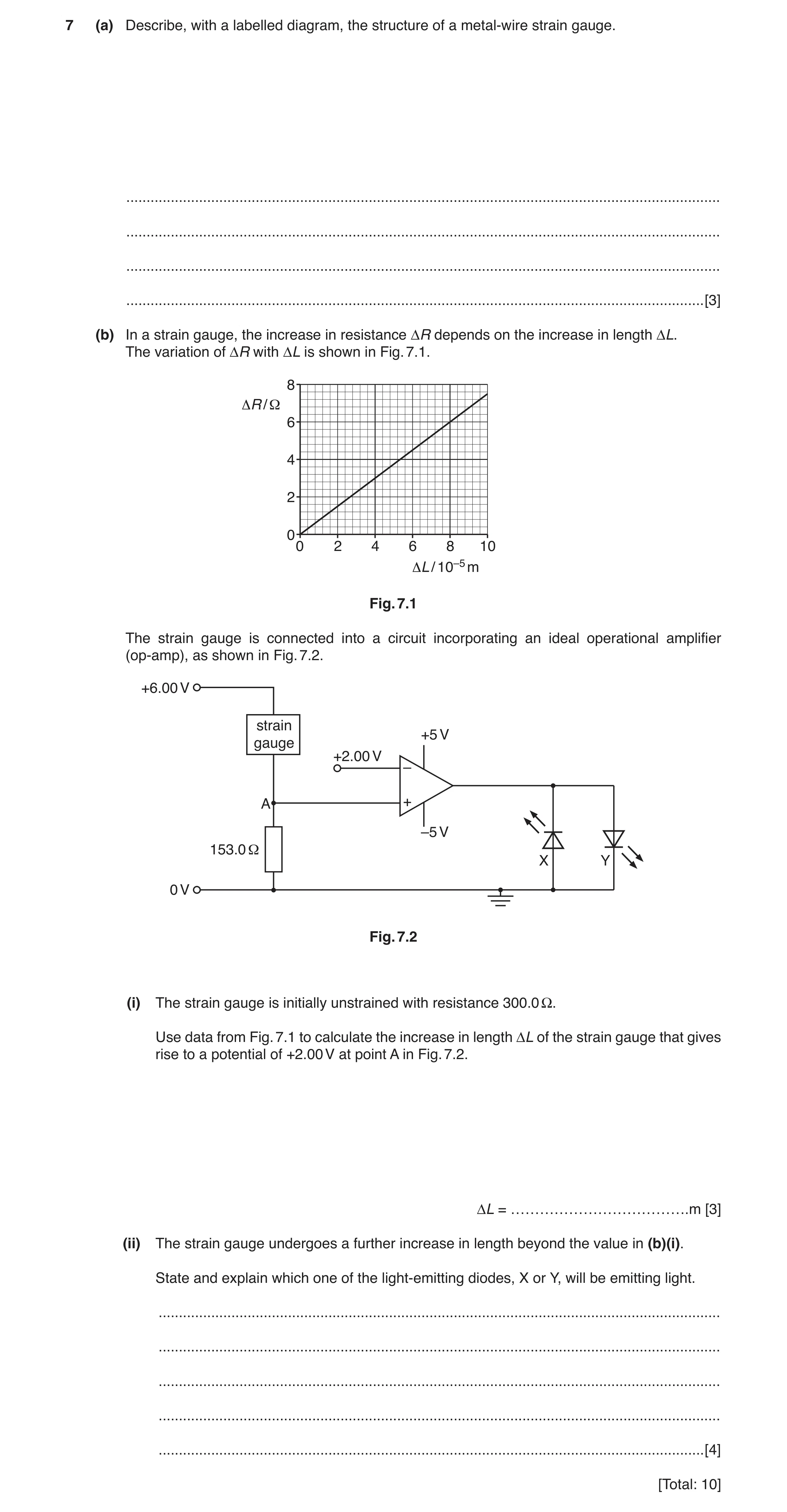
Q1 · Describe, with a labelled diagram, the structure of a metal-wire strain gauge 9702/42 Feb/March 2017
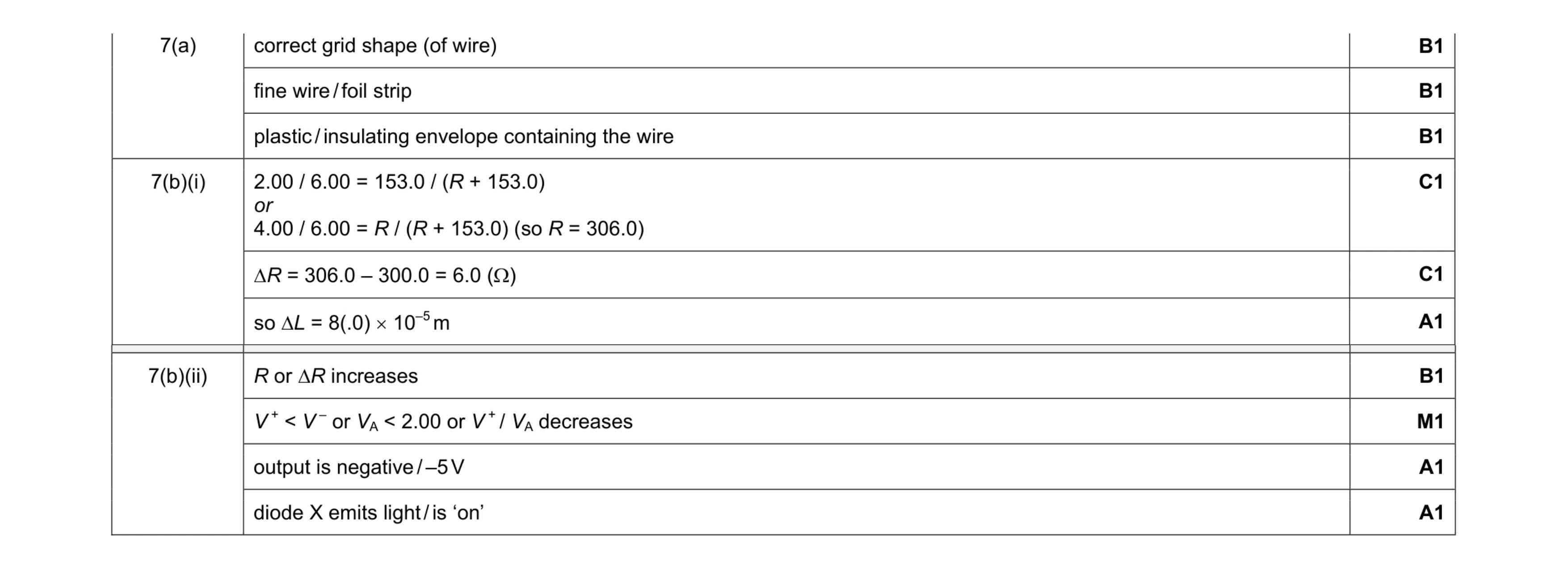
7 (a) Describe, with a labelled diagram, the structure of a metal-wire strain gauge. … … … … [3] (b) In a strain gauge, the increase in resistance ΔR depends on the increase in length ΔL. The variation of ΔR with ΔL is shown in Fig. 7.1. 8 ΔR / Ω 6 4 2 0 0 2 4 6 8 10 ΔL / 10–5 m Fig. 7.1 The strain gauge is connected into a circuit incorporating an ideal operational amplifier (op-amp), as shown in Fig. 7.2. +6.00 V strain +5 V gauge +2.00 V – A + –5 V 153.0 Ω X Y 0 V Fig. 7.2 (i) The strain gauge is initially unstrained with resistance 300.0 Ω. Use data from Fig. 7.1 to calculate the increase in length ΔL of the strain gauge that gives rise to a potential of +2.00 V at point A in Fig. 7.2. ΔL = ……………………………….m [3] (ii) The strain gauge undergoes a further increase in length beyond the value in (b)(i). State and explain which one of the light-emitting diodes, X or Y, will be emitting light. … … … … … [4] [Total: 10]
10 marks
Mark scheme: 7(a) correct grid shape (of wire) B1 fine wire / foil strip B1 plastic / insulating envelope containing the wire B1 7(b)(i) 2.00 / 6.00 = 153.0 / (R + 153.0) or 4.00 / 6.00 = R / (R + 153.0) (so R = 306.0) C1 ∆R = 306.0 – 300.0 = 6.0 (Ω) C1 so ∆L = 8(.0) × 10–5 m A1 Question Answer Marks 7(b)(ii) R or ∆R increases B1 V + < V – or VA < 2.00 or V + / VA decreases M1 output is negative / –5 V A1 diode X emits light / is ‘on’ A1
This question in 9702/42 Feb/March 2017
Q2 · A comparator circuit is designed to switch on a mains lamp when the ambient light level… 9702/41 May/June 2017
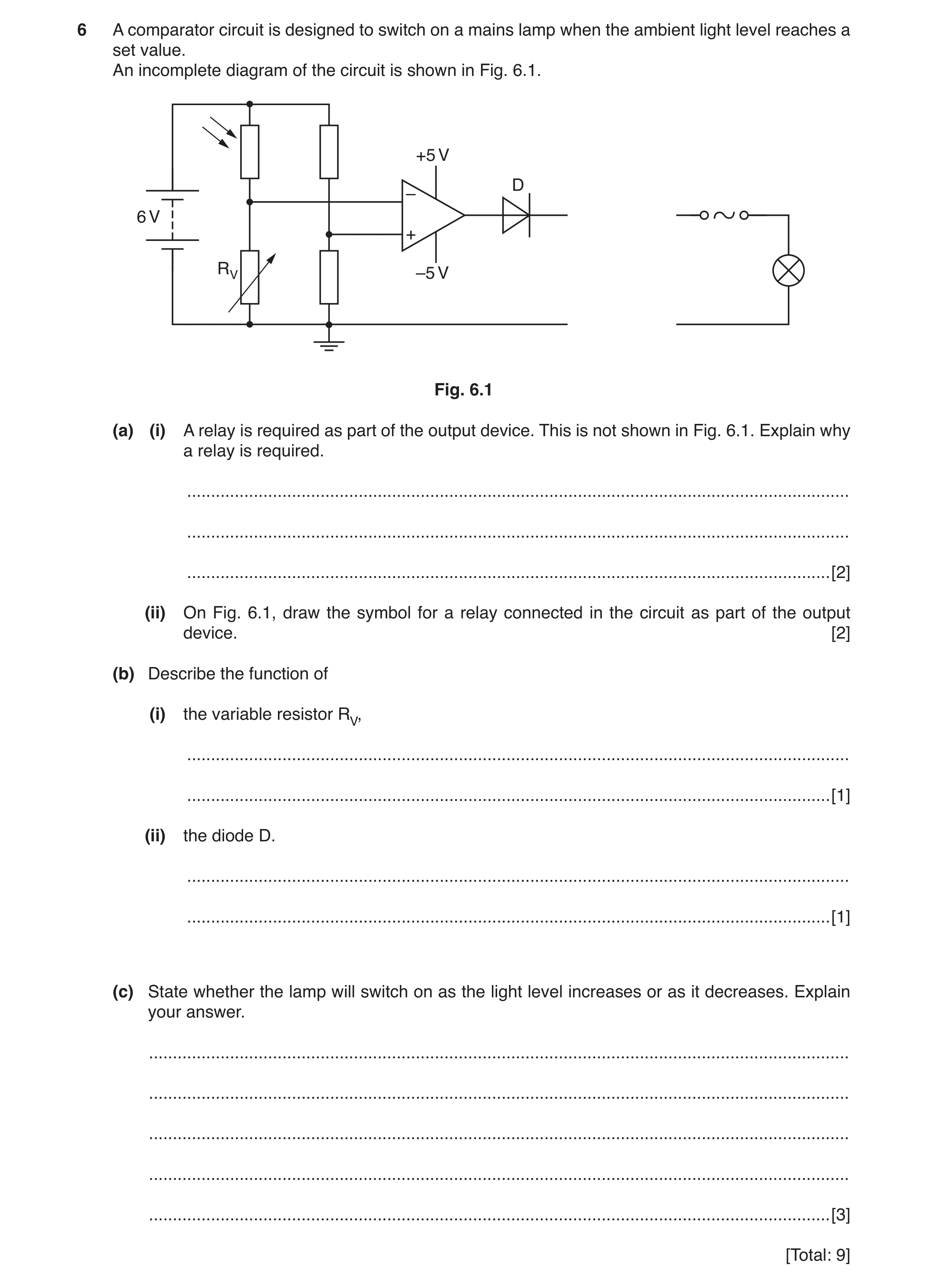
6 A comparator circuit is designed to switch on a mains lamp when the ambient light level reaches a set value. An incomplete diagram of the circuit is shown in Fig. 6.1. +5 V D – 6 V + RV –5 V Fig. 6.1 (a) (i) A relay is required as part of the output device. This is not shown in Fig. 6.1. Explain why a relay is required. … … … [2] (ii) On Fig. 6.1, draw the symbol for a relay connected in the circuit as part of the output device. [2] (b) Describe the function of (i) the variable resistor RV, … … [1] (ii) the diode D. … … [1] (c) State whether the lamp will switch on as the light level increases or as it decreases. Explain your answer. … … … … … [3] [Total: 9]
9 marks
Mark scheme: 6(a)(i) lamp needs ‘high’ power/‘large’ current/‘large’ voltage B1 op-amp can deliver only a small current/small voltage B1 6(a)(ii) correct symbol for relay coil connected between output and earth B1 switch between mains supply and lamp B1 6(b)(i) vary light intensity at which lamp is switched on/off B1 6(b)(ii) so that relay operates for only one current/voltage direction or so that relay/lamp operates for either dark or light conditions B1 6(c) when light level increases, LDR resistance decreases B1 (RLDR low,) so V – > V+, so VOUT negative/–5 V (must be consistent with B1 mark) M1 or when light level decreases, LDR resistance increases (B1) (RLDR high,) so V – < V+, so VOUT is positive/+5 V (must be consistent with B1 mark) (M1) lamp comes on as light level decreases or lamp goes off as light level increases A1
This question in 9702/41 May/June 2017
Q3 · A student designs a circuit incorporating an operational amplifier (op-amp) as shown in… 9702/42 May/June 2017
8 A student designs a circuit incorporating an operational amplifier (op-amp) as shown in Fig. 8.1. +6 V component C X R +5 V – + Y R –5 V B G RV 0 V Fig. 8.1 (a) (i) On Fig. 8.1, draw a circle around the output device. [1] (ii) State the purpose of this circuit. … … … [2] (b) The resistors X and Y each have resistance R. When conducting, the LED labelled B emits blue light and the LED labelled G emits green light. (i) State whether blue light or green light is emitted when the resistance of component C is greater than the resistance RV of the variable resistor. Explain your answer. … … … … … [3] (ii) State and explain what is observed as the resistance of component C is reduced. … … … … … [3] (c) Suggest the function of the variable resistor. … … [1] [Total: 10]
10 marks
Mark scheme: 8(a)(i) circle around both diodes B1 8(a)(ii) indicates (whether) temperature M1 (is) above or below a set value A1 8(b)(i) (when resistance of C > RV,) V– > V+ or V+ < 3 V or p.d. across RV < p.d. across R/Y/3 V or p.d. across C > p.d. across R/ X/3 V M1 op-amp output is negative M1 (only) green A1 8(b)(ii) resistance of C becomes less than RV or V– < V+ B1 green (LED) goes out A1 blue (LED) comes on A1 8(c) changes/determines temperature at which LEDs switch B1
This question in 9702/42 May/June 2017
Q4 · A comparator circuit is designed to switch on a mains lamp when the ambient light level… 9702/43 May/June 2017
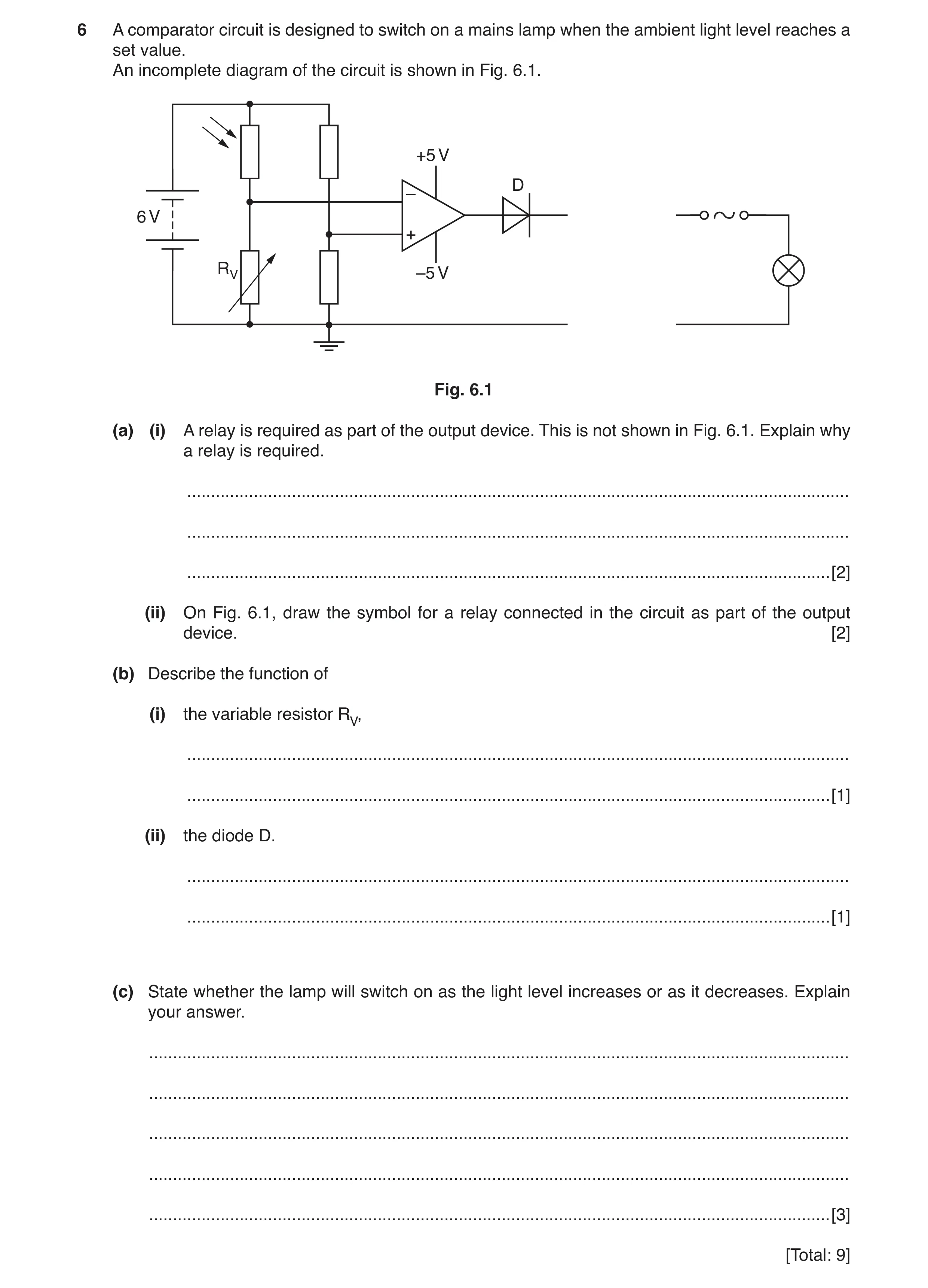
6 A comparator circuit is designed to switch on a mains lamp when the ambient light level reaches a set value. An incomplete diagram of the circuit is shown in Fig. 6.1. +5 V D – 6 V + RV –5 V Fig. 6.1 (a) (i) A relay is required as part of the output device. This is not shown in Fig. 6.1. Explain why a relay is required. … … … [2] (ii) On Fig. 6.1, draw the symbol for a relay connected in the circuit as part of the output device. [2] (b) Describe the function of (i) the variable resistor RV, … … [1] (ii) the diode D. … … [1] (c) State whether the lamp will switch on as the light level increases or as it decreases. Explain your answer. … … … … … [3] [Total: 9]
9 marks
Mark scheme: 6(a)(i) lamp needs ‘high’ power/‘large’ current/‘large’ voltage B1 op-amp can deliver only a small current/small voltage B1 6(a)(ii) correct symbol for relay coil connected between output and earth B1 switch between mains supply and lamp B1 6(b)(i) vary light intensity at which lamp is switched on/off B1 6(b)(ii) so that relay operates for only one current/voltage direction or so that relay/lamp operates for either dark or light conditions B1 6(c) when light level increases, LDR resistance decreases B1 (RLDR low,) so V – > V+, so VOUT negative/–5 V (must be consistent with B1 mark) M1 or when light level decreases, LDR resistance increases (B1) (RLDR high,) so V – < V+, so VOUT is positive/+5 V (must be consistent with B1 mark) (M1) lamp comes on as light level decreases or lamp goes off as light level increases A1
This question in 9702/43 May/June 2017
Q5 · The circuit of an amplifier incorporating an ideal operational amplifier (op-amp) is… 9702/41 Oct/Nov 2017
7 The circuit of an amplifier incorporating an ideal operational amplifier (op-amp) is shown in Fig. 7.1. R2 +9.0 V R1 P – + V IN –9.0 V V OUT Fig. 7.1 (a) By reference to the properties of an ideal op-amp, (i) explain why point P is referred to as a virtual earth, … … … … … [4] (ii) derive an expression, in terms of the resistances R1 and R2, for the gain of the amplifier circuit. [4] R2(b) In the circuit of Fig. 7.1, the ratio is 4.5. R1 The variation with time t of the input potential VIN is shown in Fig. 7.2. 14 12 10 8 6 potential / V 4 2 VINVIN 0 t –2 –4 –6 –8 –10 –12 –14 Fig. 7.2 On Fig. 7.2, show the variation with time t of the output potential VOUT. [3] [Total: 11]
11 marks
Mark scheme: 7(a)(i) gain of amplifier is very large B1 V+ is at earth (potential) B1 for amplifier not to saturate M1 difference between V– and V+ must be very small or V– must be equal to V+ A1 or if V– ≠ V+ then feedback voltage (M1) acts to reduce gap until V– = V+ when stable (A1) 7(a)(ii) input impedance is infinite B1 (so) current in R1 = current in R2 B1 (VIN – 0) / R1 = (0 – VOUT) / R2 B1 (gain =) VOUT / VIN = – R2 / R1 B1 7(b) graph: correct inverted shape (straight diagonal line from (0,0) to a negative potential, then a horizontal line, then a straight diagonal line back to the t-axis at the point where VIN = 0) B1 horizontal line at correct potential of (–)9.0 V B1 both ends of horizontal line occur at correct times (coinciding with when VIN = 2.0 V) B1
This question in 9702/41 Oct/Nov 2017
Q6 · A circuit incorporating an ideal operational amplifier (op-amp) is shown in Fig 9702/42 Oct/Nov 2018
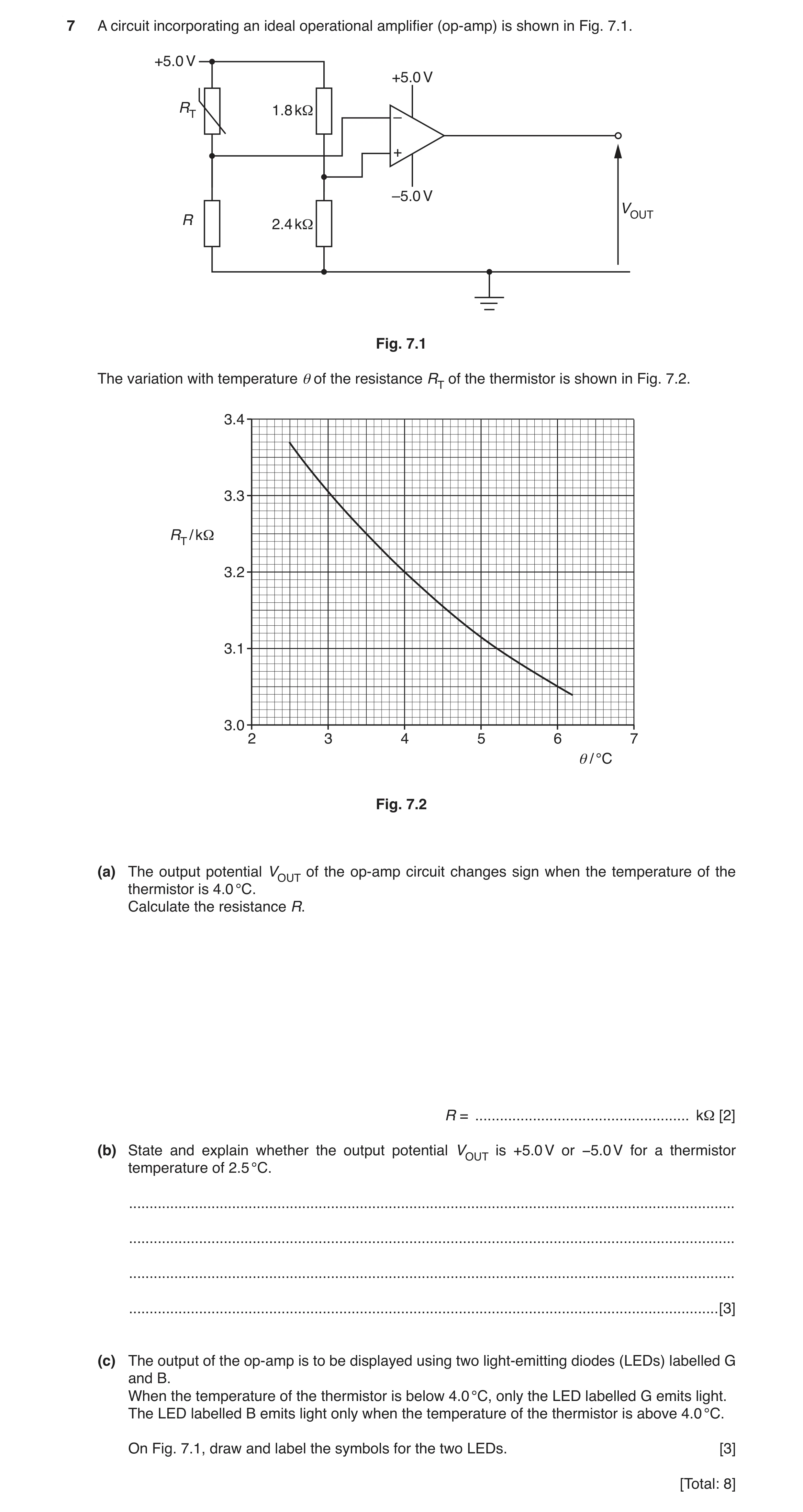
7 A circuit incorporating an ideal operational amplifier (op-amp) is shown in Fig. 7.1. +5.0 V +5.0 V RT 1.8 kΩ – + –5.0 V VOUT R 2.4 kΩ Fig. 7.1 The variation with temperature θ of the resistance RT of the thermistor is shown in Fig. 7.2. 3.4 3.3 Ω RT / k 3.2 3.1 3.0 2 3 4 5 6 7 θ / °C Fig. 7.2 (a) The output potential VOUT of the op-amp circuit changes sign when the temperature of the thermistor is 4.0 °C. Calculate the resistance R. R = … kΩ [2] (b) State and explain whether the output potential VOUT is +5.0 V or −5.0 V for a thermistor temperature of 2.5 °C. … … … … [3] (c) The output of the op-amp is to be displayed using two light-emitting diodes (LEDs) labelled G and B. When the temperature of the thermistor is below 4.0 °C, only the LED labelled G emits light. The LED labelled B emits light only when the temperature of the thermistor is above 4.0 °C. On Fig. 7.1, draw and label the symbols for the two LEDs. [3] [Total: 8]
8 marks
Mark scheme: 7(a) R / RT = 2.4 / 1.8 or at 4.0 °C, RT = 3.2 kΩ C1 hence R / 3.2 = 2.4 / 1.8 R = 4.3 kΩ A1 7(b) RT = 3.37 kΩ or RT is greater (than 3.2 kΩ) B1 V+ > V– M1 hence output is +5.0 V A1 Question Answer Marks 7(c) correct LED symbol B1 two diodes shown connected, in parallel and with opposite polarities, between VOUT and earth M1 diodes labelled to show correct polarities consistent with (b) (G pointing from VOUT to earth and B pointing from earth to VOUT if (b) correct) A1
This question in 9702/42 Oct/Nov 2018
Q7 · Use band theory to explain why the resistance of an intrinsic semiconductor decreases as… 9702/42 May/June 2019
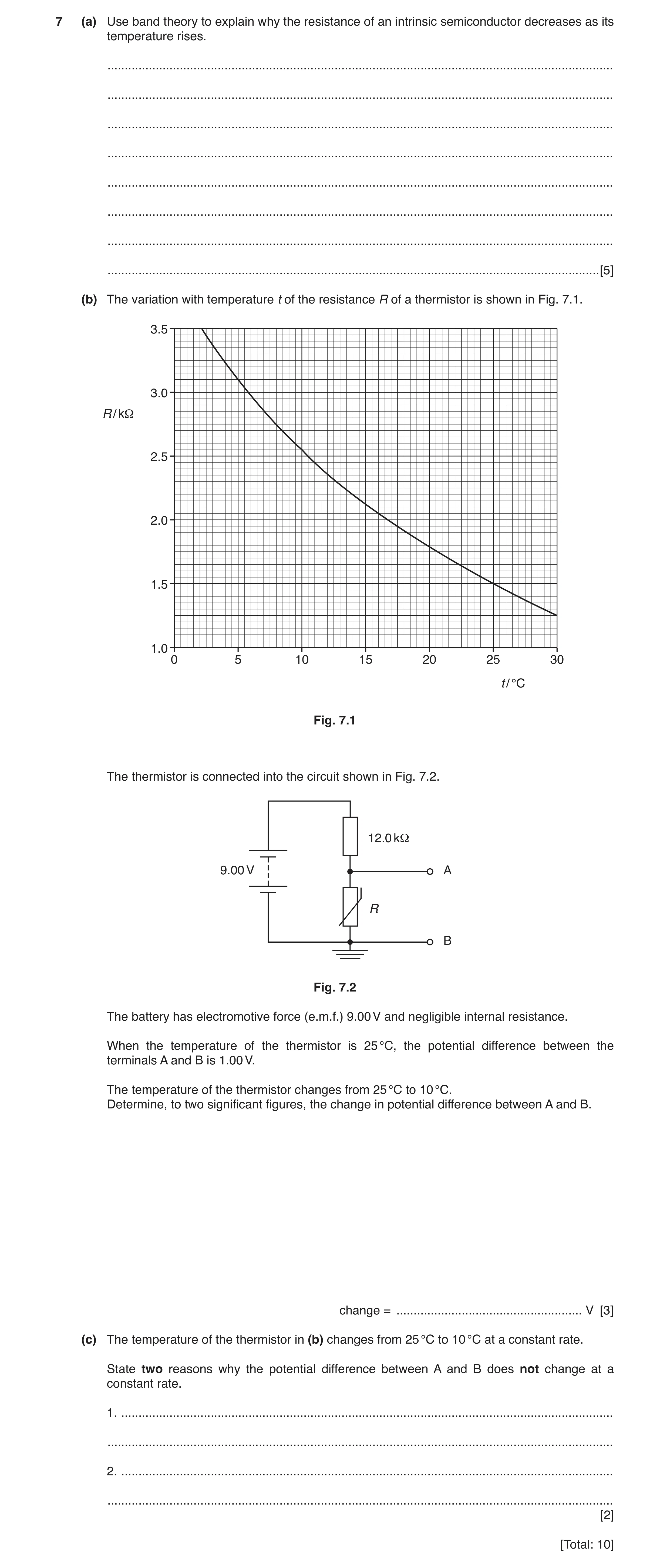
7 (a) Use band theory to explain why the resistance of an intrinsic semiconductor decreases as its temperature rises. … … … … … … … … [5] (b) The variation with temperature t of the resistance R of a thermistor is shown in Fig. 7.1. 3.5 3.0 R / kΩ 2.5 2.0 1.5 1.0 0 5 10 15 20 25 30 t / °C Fig. 7.1 The thermistor is connected into the circuit shown in Fig. 7.2. 12.0 kΩ 9.00 V A R B Fig. 7.2 The battery has electromotive force (e.m.f.) 9.00 V and negligible internal resistance. When the temperature of the thermistor is 25 °C, the potential difference between the terminals A and B is 1.00 V. The temperature of the thermistor changes from 25 °C to 10 °C. Determine, to two significant figures, the change in potential difference between A and B. change = … V [3] (c) The temperature of the thermistor in (b) changes from 25 °C to 10 °C at a constant rate. State two reasons why the potential difference between A and B does not change at a constant rate. 1. … … 2. … … [2] [Total: 10]
10 marks
Mark scheme: 7(a) Any five from: • (as temperature rises) energy of electrons increases • electrons (have enough energy to) cross forbidden band • electrons enter conduction band • leaving holes in valence band • both holes and electrons act as charge carriers • more charge carriers results in lower resistance • increased lattice vibrations outweighed by increase in (number of) charge carriers B5 7(b) (at 10 °C resistance is) 2.55 kΩ C1 new potential difference = 9.00 × 2.55 / (2.55 + 12.0) = 1.58 V C1 change in p.d. = 0.58 V A1 7(c) change of resistance with temperature is not linear B1 change in potential with resistance is not linear or potential divider equation is non-linear B1
This question in 9702/42 May/June 2019
Q8 · The upper electron energy bands in an intrinsic semiconductor material are illustrated in… 9702/42 Oct/Nov 2019
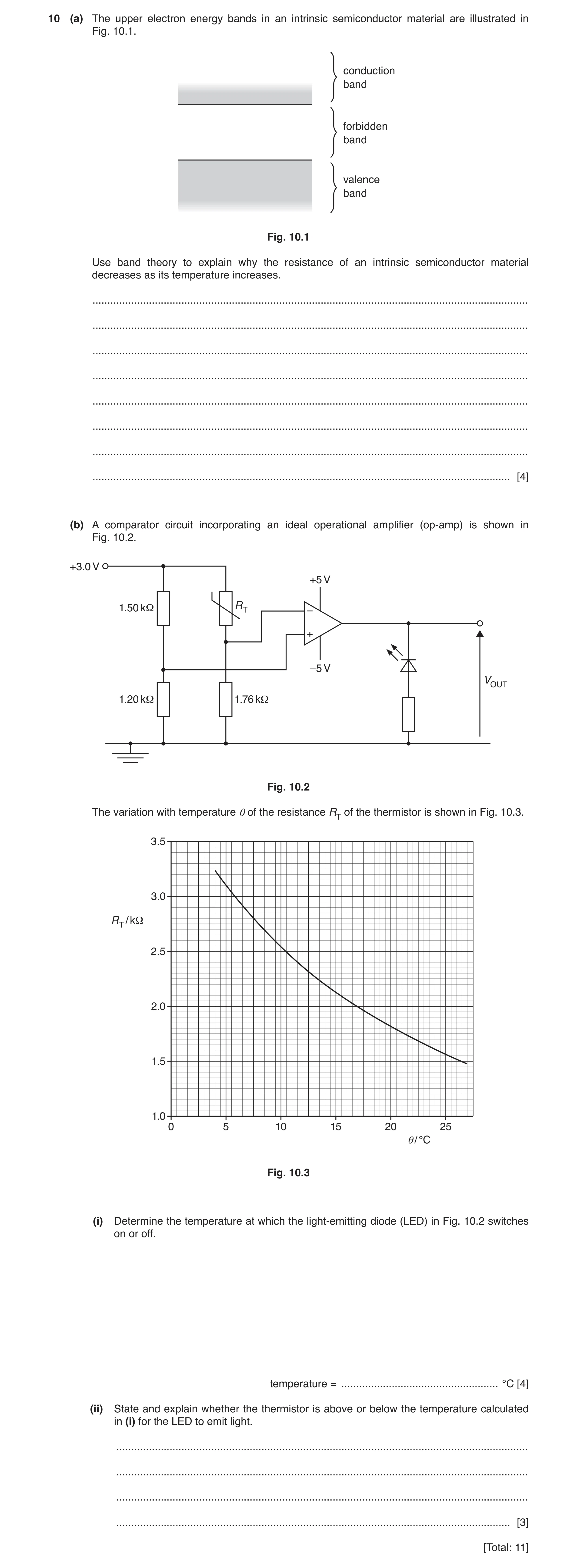
10 (a) The upper electron energy bands in an intrinsic semiconductor material are illustrated in Fig. 10.1. conduction band forbidden band valence band Fig. 10.1 Use band theory to explain why the resistance of an intrinsic semiconductor material decreases as its temperature increases. … … … … … … … … [4] (b) A comparator circuit incorporating an ideal operational amplifier (op-amp) is shown in Fig. 10.2. +3.0 V +5 V 1.50 kΩ RT –5 V VOUT 1.20 kΩ 1.76 kΩ Fig. 10.2 The variation with temperature θ of the resistance RT of the thermistor is shown in Fig. 10.3. 3.5 3.0 RT / kΩ 2.5 2.0 1.5 1.0 0 5 10 15 20 25 θ/ °C Fig. 10.3 (i) Determine the temperature at which the light-emitting diode (LED) in Fig. 10.2 switches on or off. temperature = … °C [4] (ii) State and explain whether the thermistor is above or below the temperature calculated in (i) for the LED to emit light. … … … … [3] [Total: 11]
11 marks
Mark scheme: 10(a) (as temperature rises) electrons in valence band gain energy B1 electrons jump to conduction band B1 holes are left in the valence band B1 increased number (density) of charge carriers causes lower resistance B1 10(b)(i) V– = V+ C1 1.50 / 1.20 = RT / 1.76 C1 RT = 2.2 (kΩ) C1 temperature = 14 °C A1 10(b)(ii) (For LED to conduct,) VOUT must be negative B1 V– > V+ B1 RT must be lower so temperature must be above (b)(i) value B1
This question in 9702/42 Oct/Nov 2019
Question 9 9702/42 Feb/March 2020
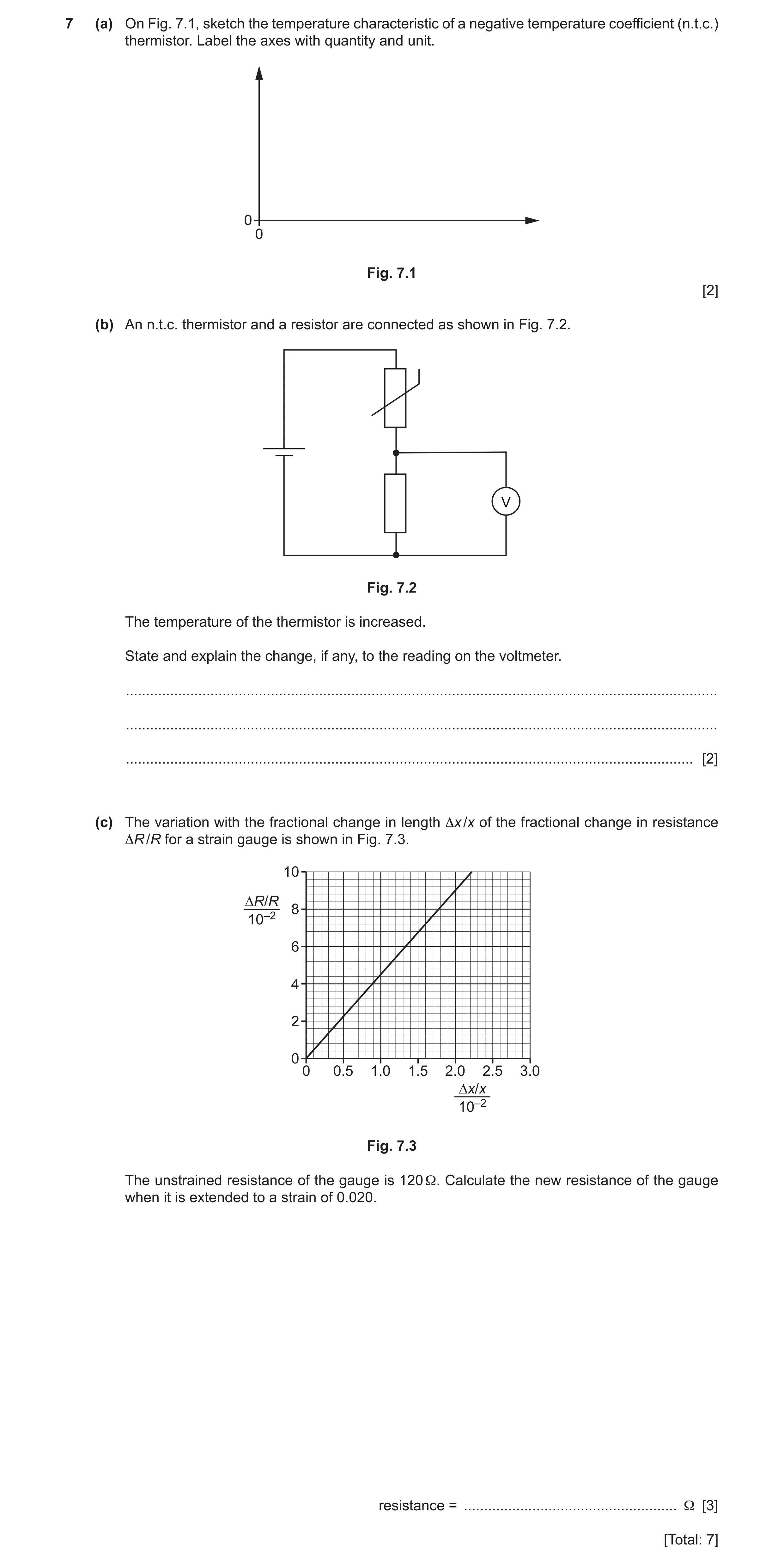
7 (a) On Fig. 7.1, sketch the temperature characteristic of a negative temperature coefficient (n.t.c.) thermistor. Label the axes with quantity and unit. 0 0 Fig. 7.1 [2] (b) An n.t.c. thermistor and a resistor are connected as shown in Fig. 7.2. V Fig. 7.2 The temperature of the thermistor is increased. State and explain the change, if any, to the reading on the voltmeter. … … … [2] (c) The variation with the fractional change in length Δx /x of the fractional change in resistance ΔR /R for a strain gauge is shown in Fig. 7.3. 10 ∆R/R 8 10–2 6 4 2 0 0 0.5 1.0 1.5 2.0 2.5 3.0 ∆x/x 10–2 Fig. 7.3 The unstrained resistance of the gauge is 120 Ω. Calculate the new resistance of the gauge when it is extended to a strain of 0.020. resistance = … Ω [3] [Total: 7]
7 marks
Mark scheme: 7(a) axes labelled with resistance and temperature M0 concave curve not touching temperature axis A1 line with negative gradient throughout A1 7(b) resistance of thermistor decreases B1 total circuit resistance decreases so voltmeter reading increases or current increases so voltmeter reading increases or greater proportion of resistance in fixed resistor so voltmeter reading increases or p.d. across thermistor decreases so voltmeter reading increases B1 7(c) (0.020 strain means) ΔR / R = 0.090 C1 ΔR = 0.090 × 120 = 10.8 Ω C1 resistance = 120 + 10.8 = 130 Ω A1
This question in 9702/42 Feb/March 2020
Q10 · The output of a microphone is processed using a non-inverting amplifier 9702/41 May/June 2020
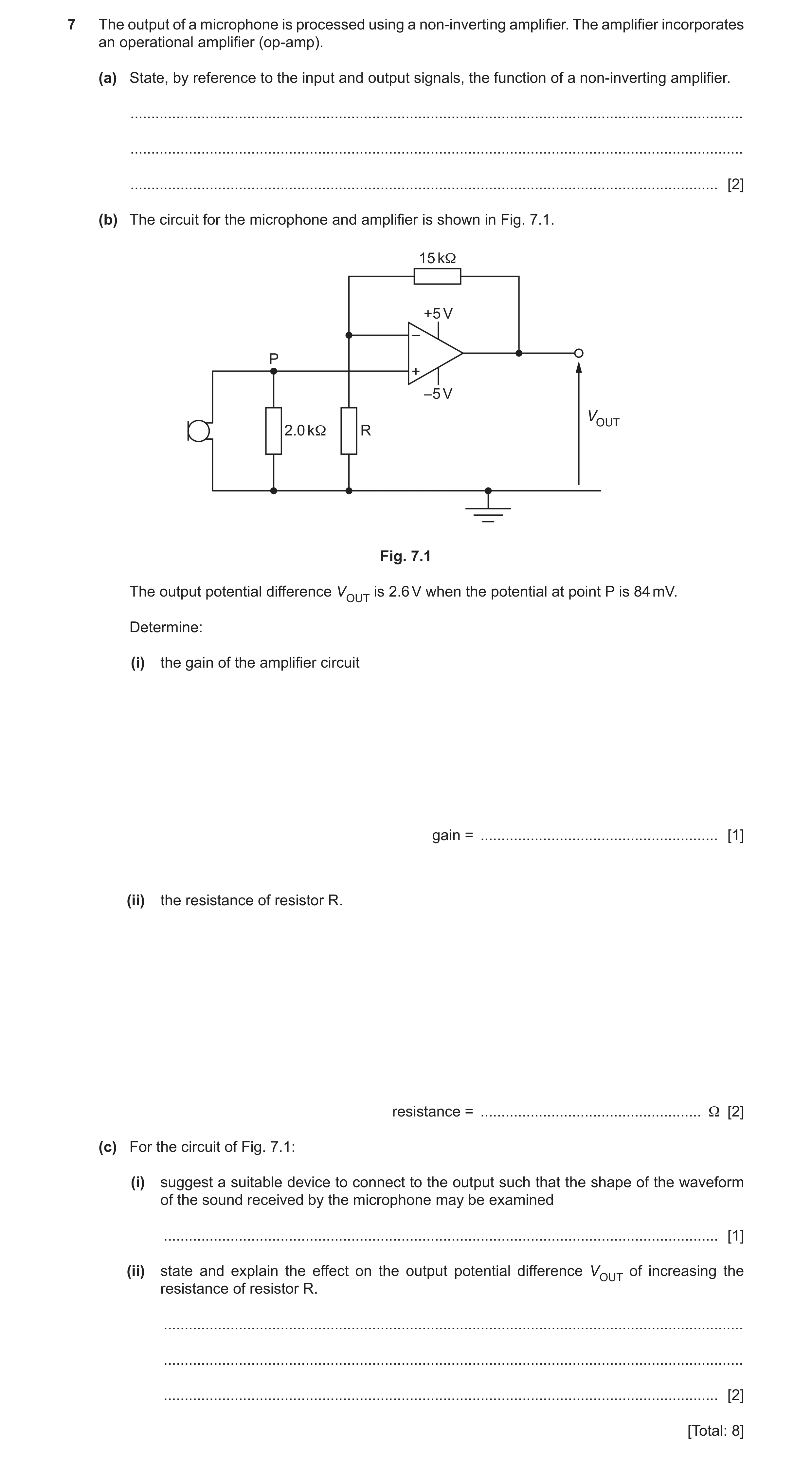
7 The output of a microphone is processed using a non-inverting amplifier. The amplifier incorporates an operational amplifier (op-amp). (a) State, by reference to the input and output signals, the function of a non-inverting amplifier. … … … [2] (b) The circuit for the microphone and amplifier is shown in Fig. 7.1. 15 kΩ +5 V – P + –5 V VOUT 2.0 kΩ R Fig. 7.1 The output potential difference VOUT is 2.6 V when the potential at point P is 84 mV. Determine: (i) the gain of the amplifier circuit gain = … [1] (ii) the resistance of resistor R. resistance = … Ω [2] (c) For the circuit of Fig. 7.1: (i) suggest a suitable device to connect to the output such that the shape of the waveform of the sound received by the microphone may be examined … [1] (ii) state and explain the effect on the output potential difference VOUT of increasing the resistance of resistor R. … … … [2] [Total: 8]
8 marks
Mark scheme: 7(a) output signal proportional to input signal B1 output signal has same sign/polarity as input signal B1 7(b)(i) gain = VOUT / VIN = 2.6 / 0.084 = 31 A1 7(b)(ii) 31 = 1 + (15 × 103) / R C1 R = 500 Ω A1 7(c)(i) e.g. cathode-ray oscilloscope/CRO B1 7(c)(ii) gain is reduced B1 (so) VOUT is smaller B1
This question in 9702/41 May/June 2020
Q11 · The output of a microphone is processed using a non-inverting amplifier 9702/43 May/June 2020
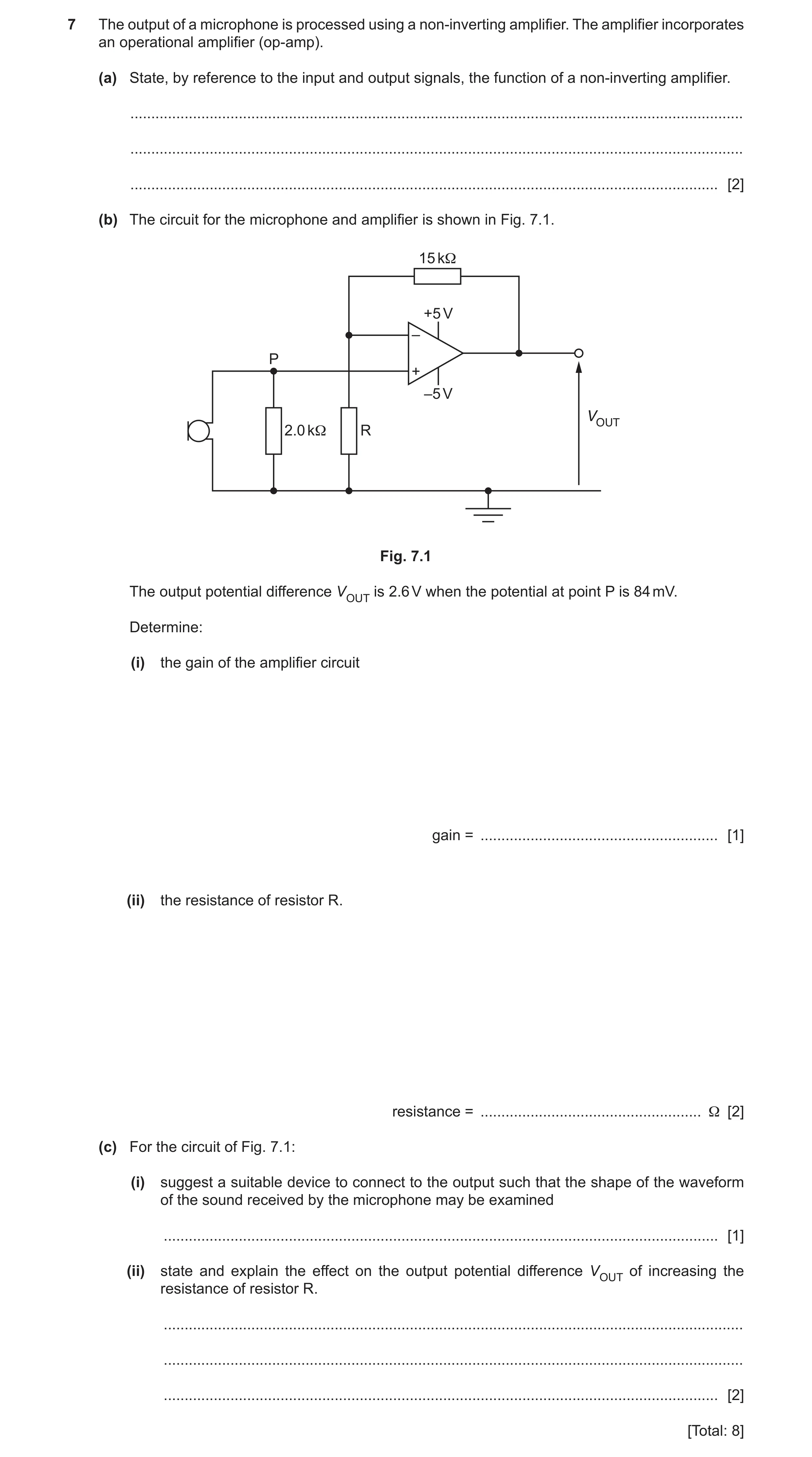
7 The output of a microphone is processed using a non-inverting amplifier. The amplifier incorporates an operational amplifier (op-amp). (a) State, by reference to the input and output signals, the function of a non-inverting amplifier. … … … [2] (b) The circuit for the microphone and amplifier is shown in Fig. 7.1. 15 kΩ +5 V – P + –5 V VOUT 2.0 kΩ R Fig. 7.1 The output potential difference VOUT is 2.6 V when the potential at point P is 84 mV. Determine: (i) the gain of the amplifier circuit gain = … [1] (ii) the resistance of resistor R. resistance = … Ω [2] (c) For the circuit of Fig. 7.1: (i) suggest a suitable device to connect to the output such that the shape of the waveform of the sound received by the microphone may be examined … [1] (ii) state and explain the effect on the output potential difference VOUT of increasing the resistance of resistor R. … … … [2] [Total: 8]
8 marks
Mark scheme: 7(a) output signal proportional to input signal B1 output signal has same sign/polarity as input signal B1 7(b)(i) gain = VOUT / VIN = 2.6 / 0.084 = 31 A1 7(b)(ii) 31 = 1 + (15 × 103) / R C1 R = 500 Ω A1 7(c)(i) e.g. cathode-ray oscilloscope/CRO B1 7(c)(ii) gain is reduced B1 (so) VOUT is smaller B1
This question in 9702/43 May/June 2020
Q12 · An ideal operational amplifier (op-amp) is to be used in a comparator circuit 9702/41 Oct/Nov 2020
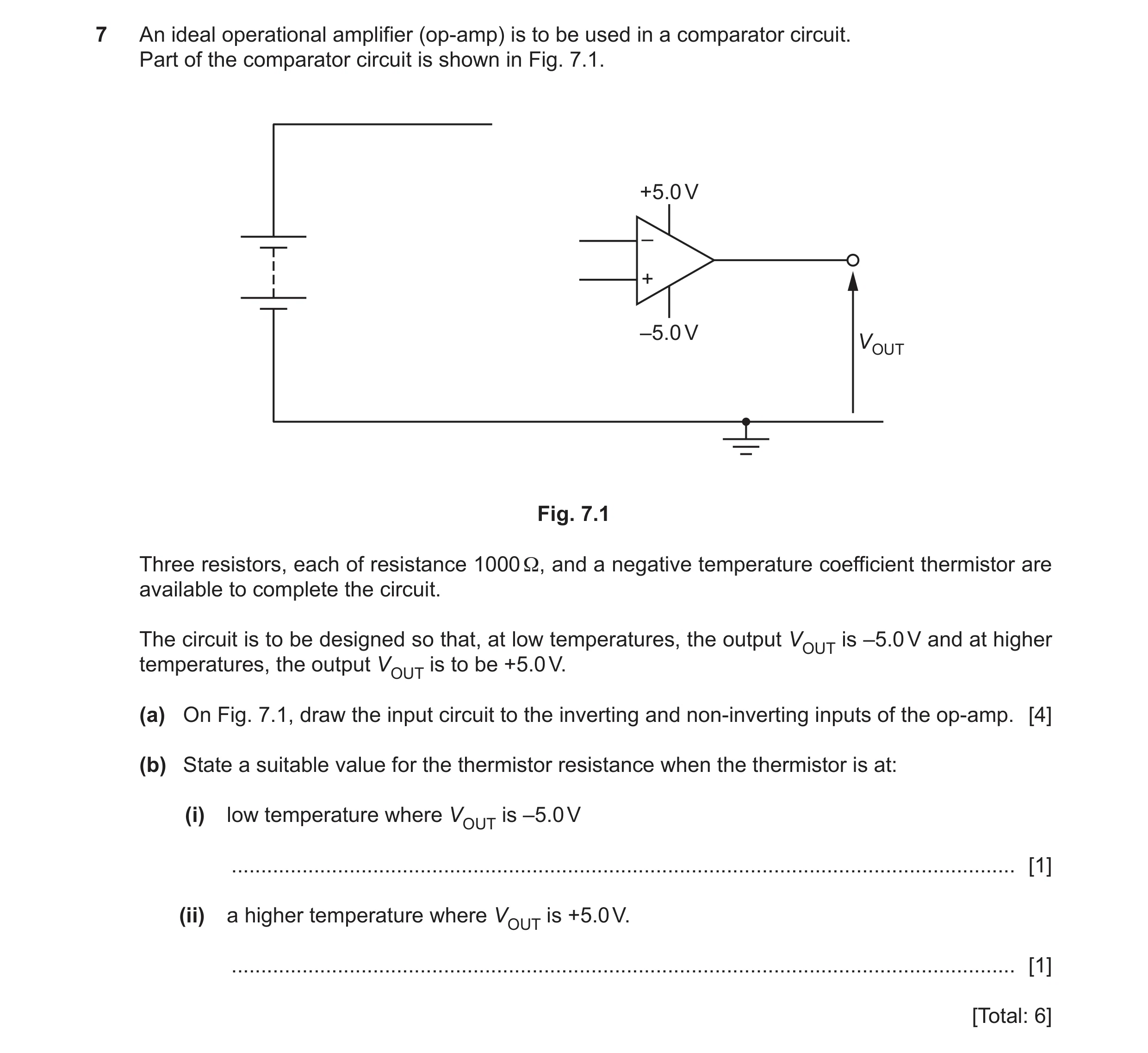
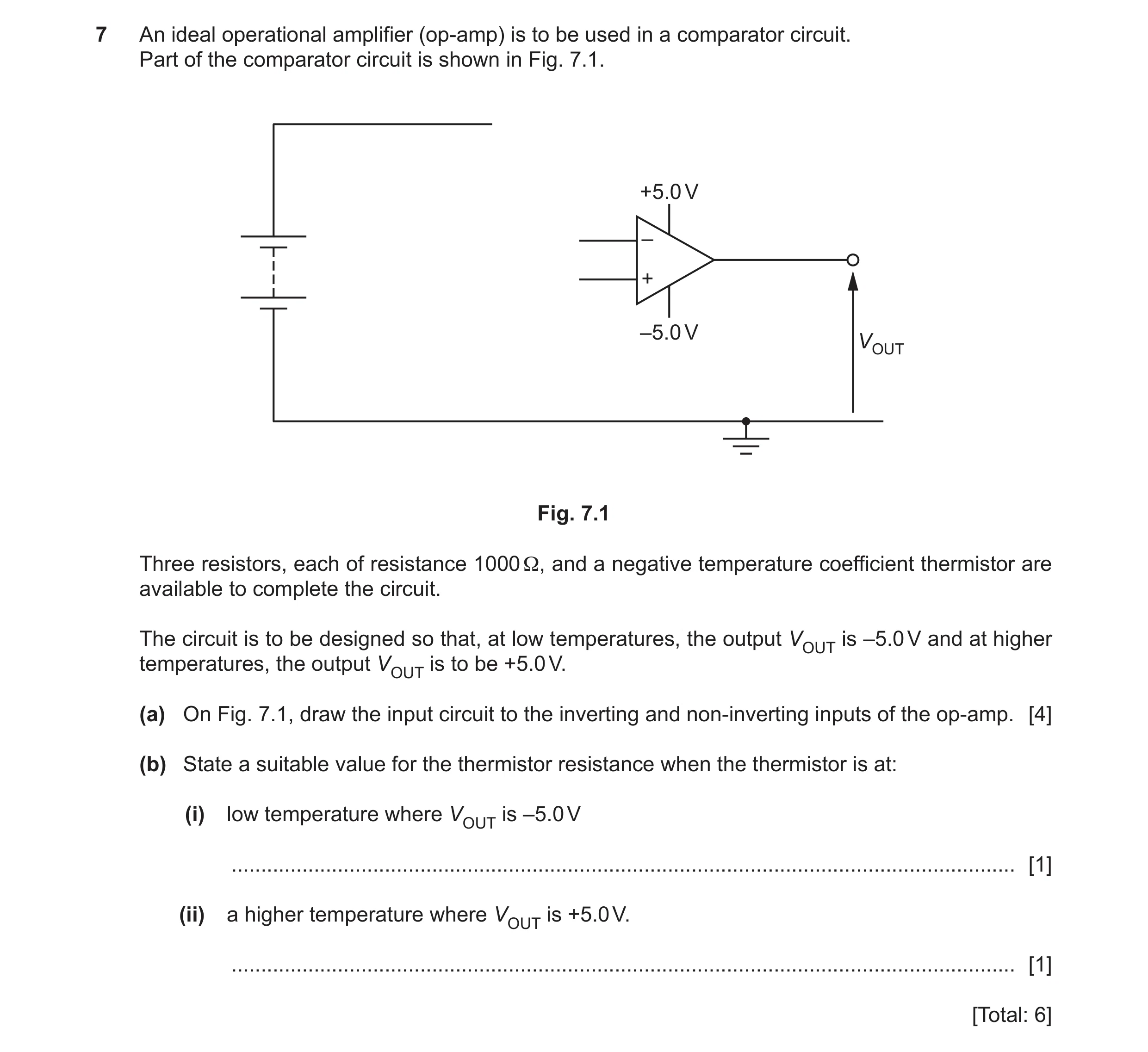
7 An ideal operational amplifier (op-amp) is to be used in a comparator circuit. Part of the comparator circuit is shown in Fig. 7.1. +5.0 V – + –5.0 V VOUT Fig. 7.1 Three resistors, each of resistance 1000 Ω, and a negative temperature coefficient thermistor are available to complete the circuit. The circuit is to be designed so that, at low temperatures, the output VOUT is –5.0 V and at higher temperatures, the output VOUT is to be +5.0 V. (a) On Fig. 7.1, draw the input circuit to the inverting and non-inverting inputs of the op-amp. [4] (b) State a suitable value for the thermistor resistance when the thermistor is at: (i) low temperature where VOUT is –5.0 V … [1] (ii) a higher temperature where VOUT is +5.0 V. … [1] [Total: 6]
6 marks
Mark scheme: 7(a) two resistors connected in series between earth and positive of battery and no extra connections B1 one resistor and thermistor connected in series between earth and positive of battery and no extra connections B1 midpoints of the two potential dividers connected, one each, to the op-amp input terminals B1 thermistor in correct place in potential divider circuit (either the upper part of the potential divider leading to V+ or the lower part of the potential divider leading to V–) B1 7(b)(i) value greater than 1000 Ω A1 7(b)(ii) non-zero value less than 1000 Ω A1
This question in 9702/41 Oct/Nov 2020
Q13 · An ideal operational amplifier (op-amp) is to be used in a comparator circuit 9702/43 Oct/Nov 2020
7 An ideal operational amplifier (op-amp) is to be used in a comparator circuit. Part of the comparator circuit is shown in Fig. 7.1. +5.0 V – + –5.0 V VOUT Fig. 7.1 Three resistors, each of resistance 1000 Ω, and a negative temperature coefficient thermistor are available to complete the circuit. The circuit is to be designed so that, at low temperatures, the output VOUT is –5.0 V and at higher temperatures, the output VOUT is to be +5.0 V. (a) On Fig. 7.1, draw the input circuit to the inverting and non-inverting inputs of the op-amp. [4] (b) State a suitable value for the thermistor resistance when the thermistor is at: (i) low temperature where VOUT is –5.0 V … [1] (ii) a higher temperature where VOUT is +5.0 V. … [1] [Total: 6]
6 marks
Mark scheme: 7(a) two resistors connected in series between earth and positive of battery and no extra connections B1 one resistor and thermistor connected in series between earth and positive of battery and no extra connections B1 midpoints of the two potential dividers connected, one each, to the op-amp input terminals B1 thermistor in correct place in potential divider circuit (either the upper part of the potential divider leading to V+ or the lower part of the potential divider leading to V–) B1 7(b)(i) value greater than 1000 Ω A1 7(b)(ii) non-zero value less than 1000 Ω A1
This question in 9702/43 Oct/Nov 2020
Q14 · The variation with temperature of the resistance of a thermistor is shown in Fig 9702/41 May/June 2021
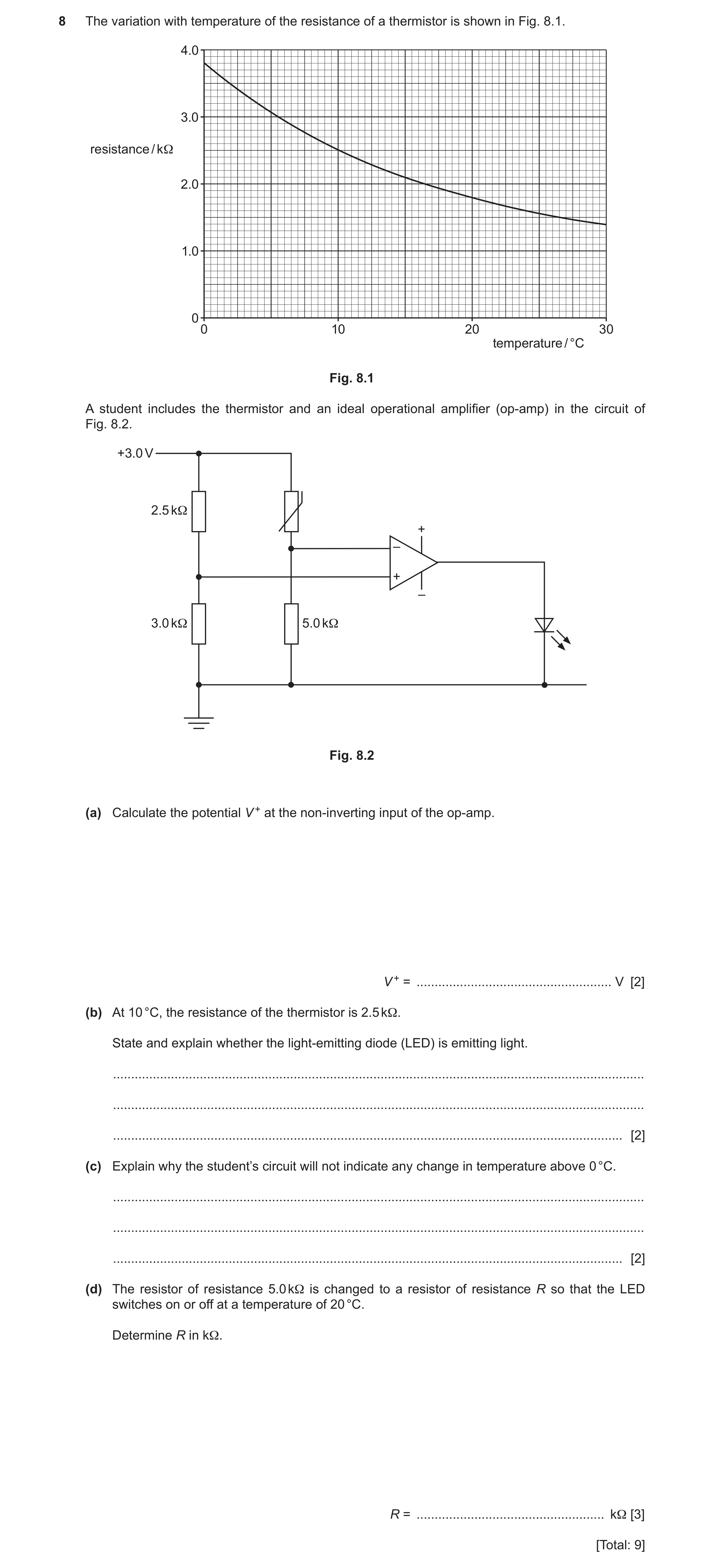
8 The variation with temperature of the resistance of a thermistor is shown in Fig. 8.1. 4.0 3.0 resistance / kΩ 2.0 1.0 0 0 10 20 30 temperature / °C Fig. 8.1 A student includes the thermistor and an ideal operational amplifier (op-amp) in the circuit of Fig. 8.2. +3.0 V 2.5 kΩ + – + – 3.0 kΩ 5.0 kΩ Fig. 8.2 (a) Calculate the potential V + at the non-inverting input of the op-amp. V + = … V [2] (b) At 10 °C, the resistance of the thermistor is 2.5 kΩ. State and explain whether the light-emitting diode (LED) is emitting light. … … … [2] (c) Explain why the student’s circuit will not indicate any change in temperature above 0 °C. … … … [2] (d) The resistor of resistance 5.0 kΩ is changed to a resistor of resistance R so that the LED switches on or off at a temperature of 20 °C. Determine R in kΩ. R = … kΩ [3] [Total: 9]
9 marks
Mark scheme: 8(a) V+ = 3.0 × 3.0 / (2.5 + 3.0) = 1.6 V A1 8(b) V – is +2.0 V or V – > V + B1 output is negative so (LED) does not emit light B1 8(c) at 0 °C, V – = 1.7 V or for all temperatures above 0 °C, resistance of thermistor < 4.2 kΩ B1 V – always greater than V + (so no switching) B1 8(d) (at 20 °C,) RT = 1.8 kΩ C1 2.5 / 3.0 = 1.8 / R or [R / (R + 1.8)] × 3.0 = 1.6 C1 R = 2.2 kΩ A1
This question in 9702/41 May/June 2021
Q15 · The variation with temperature of the resistance of a thermistor is shown in Fig 9702/43 May/June 2021
8 The variation with temperature of the resistance of a thermistor is shown in Fig. 8.1. 4.0 3.0 resistance / kΩ 2.0 1.0 0 0 10 20 30 temperature / °C Fig. 8.1 A student includes the thermistor and an ideal operational amplifier (op-amp) in the circuit of Fig. 8.2. +3.0 V 2.5 kΩ + – + – 3.0 kΩ 5.0 kΩ Fig. 8.2 (a) Calculate the potential V + at the non-inverting input of the op-amp. V + = … V [2] (b) At 10 °C, the resistance of the thermistor is 2.5 kΩ. State and explain whether the light-emitting diode (LED) is emitting light. … … … [2] (c) Explain why the student’s circuit will not indicate any change in temperature above 0 °C. … … … [2] (d) The resistor of resistance 5.0 kΩ is changed to a resistor of resistance R so that the LED switches on or off at a temperature of 20 °C. Determine R in kΩ. R = … kΩ [3] [Total: 9]
9 marks
Mark scheme: 8(a) V+ = 3.0 × 3.0 / (2.5 + 3.0) = 1.6 V A1 8(b) V – is +2.0 V or V – > V + B1 output is negative so (LED) does not emit light B1 8(c) at 0 °C, V – = 1.7 V or for all temperatures above 0 °C, resistance of thermistor < 4.2 kΩ B1 V – always greater than V + (so no switching) B1 8(d) (at 20 °C,) RT = 1.8 kΩ C1 2.5 / 3.0 = 1.8 / R or [R / (R + 1.8)] × 3.0 = 1.6 C1 R = 2.2 kΩ A1
This question in 9702/43 May/June 2021
 3 / 23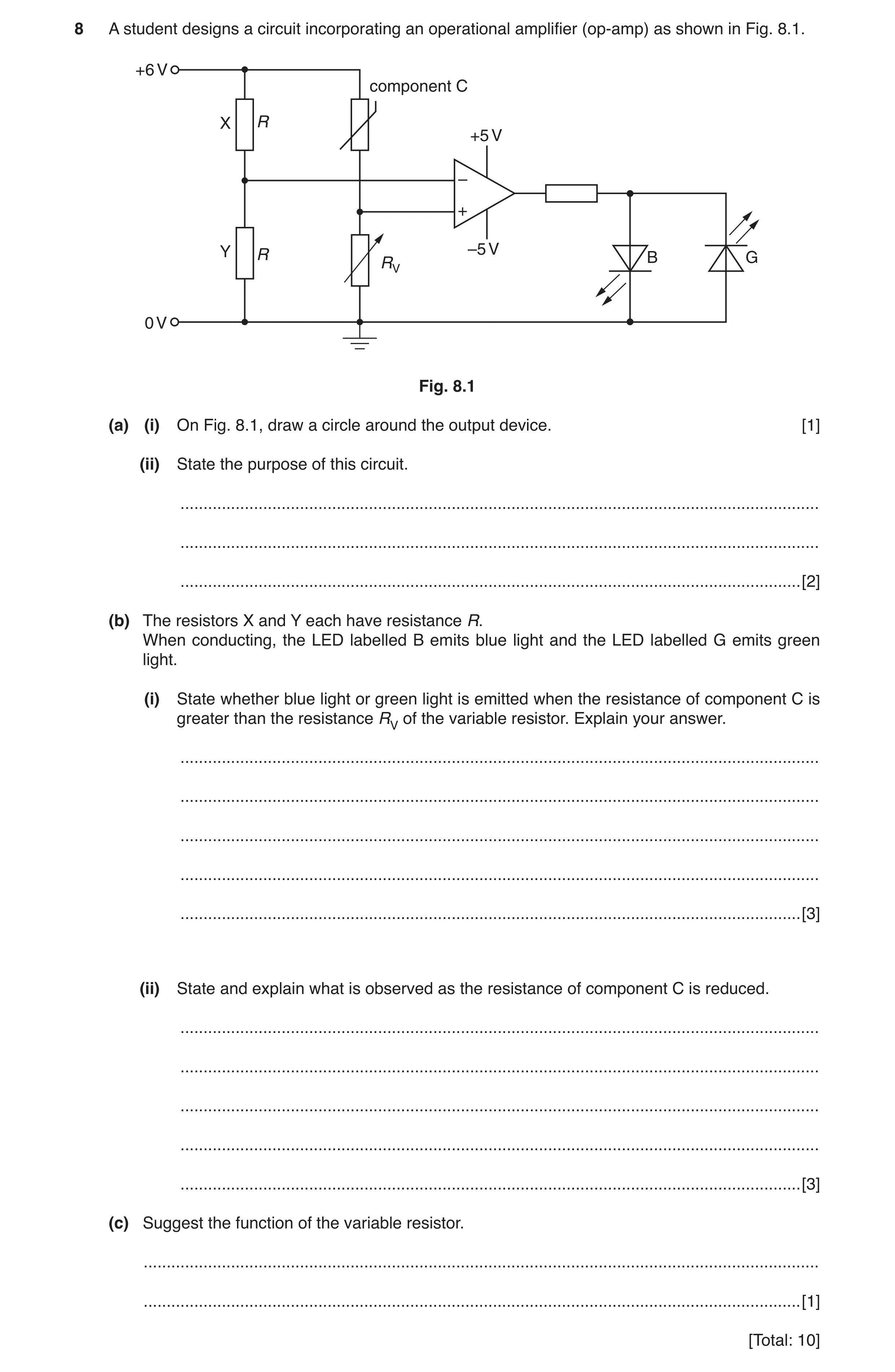
 6 / 23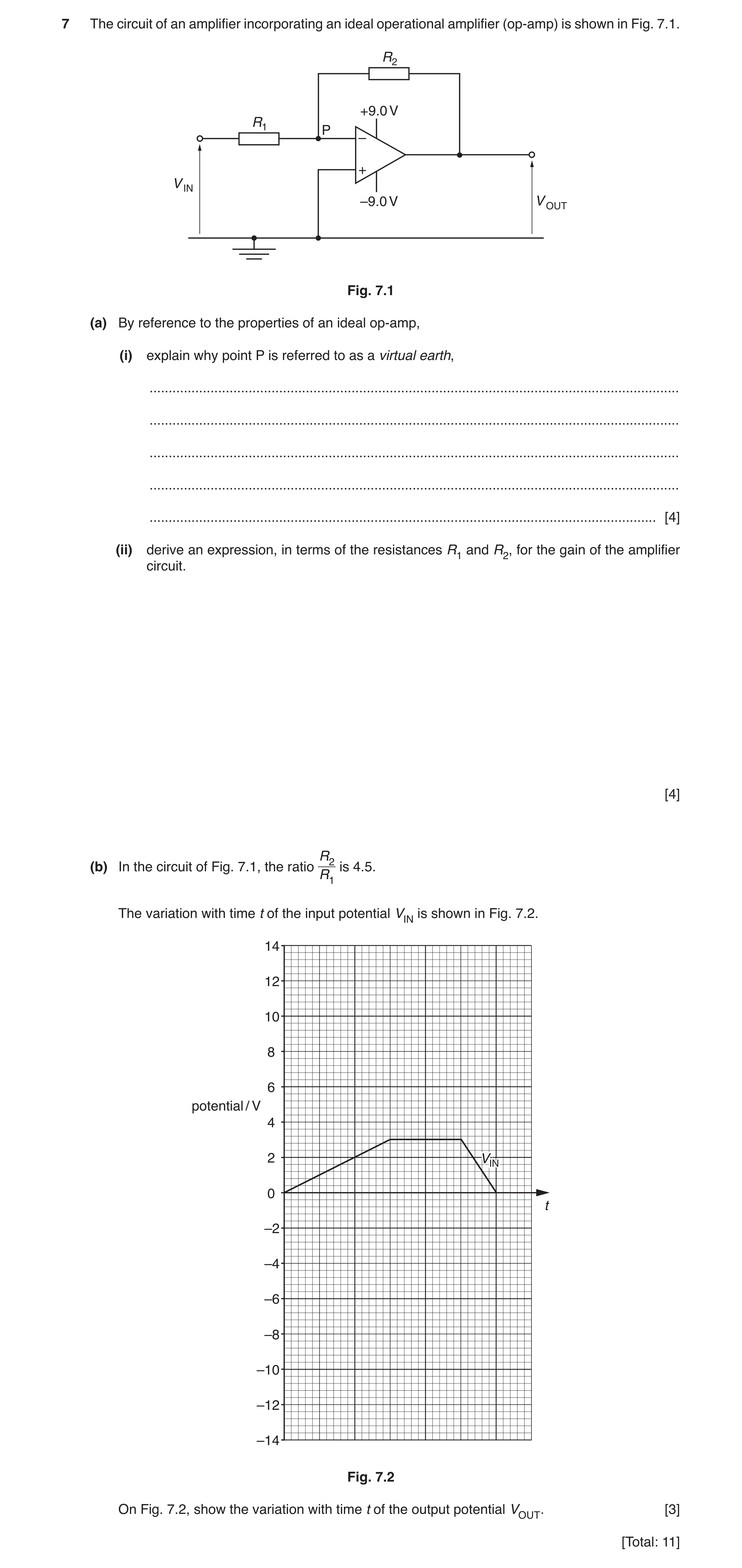
 18 / 23
 19 / 23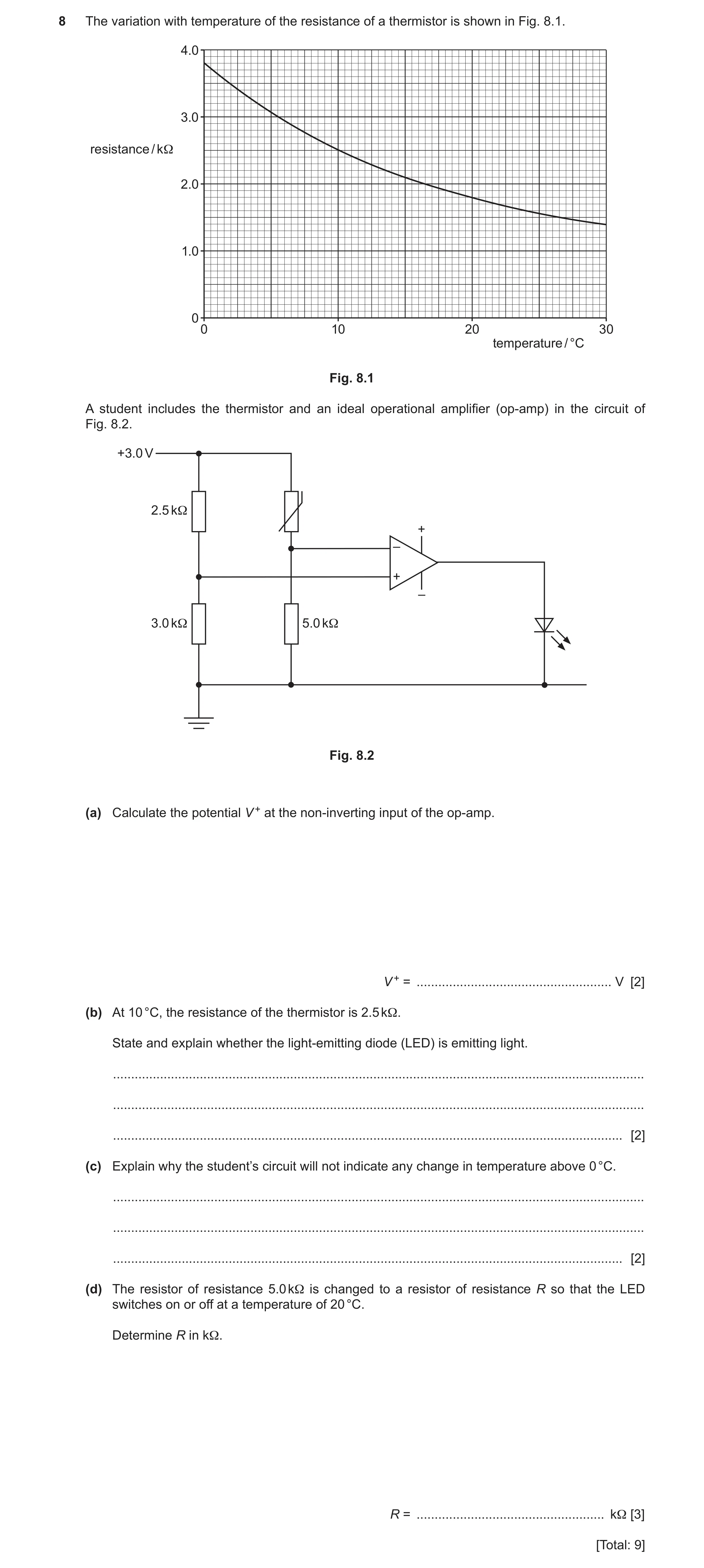
 10
10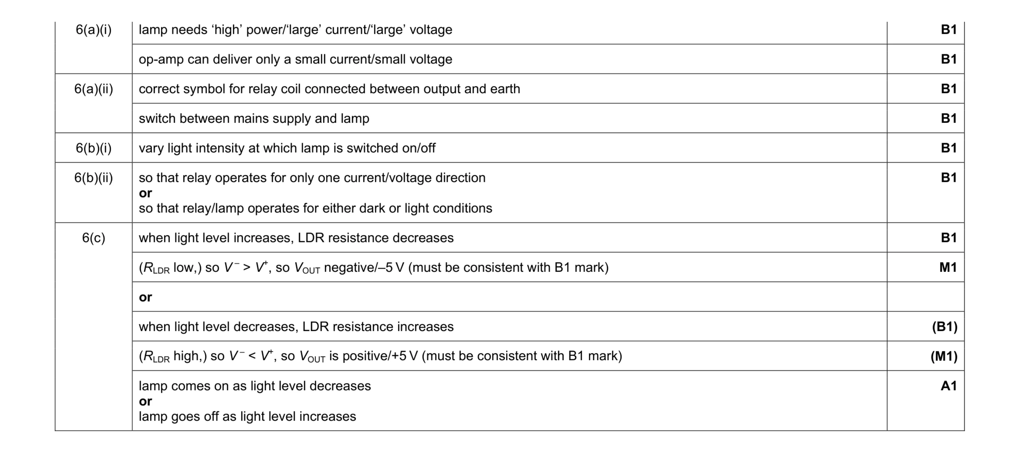 9
9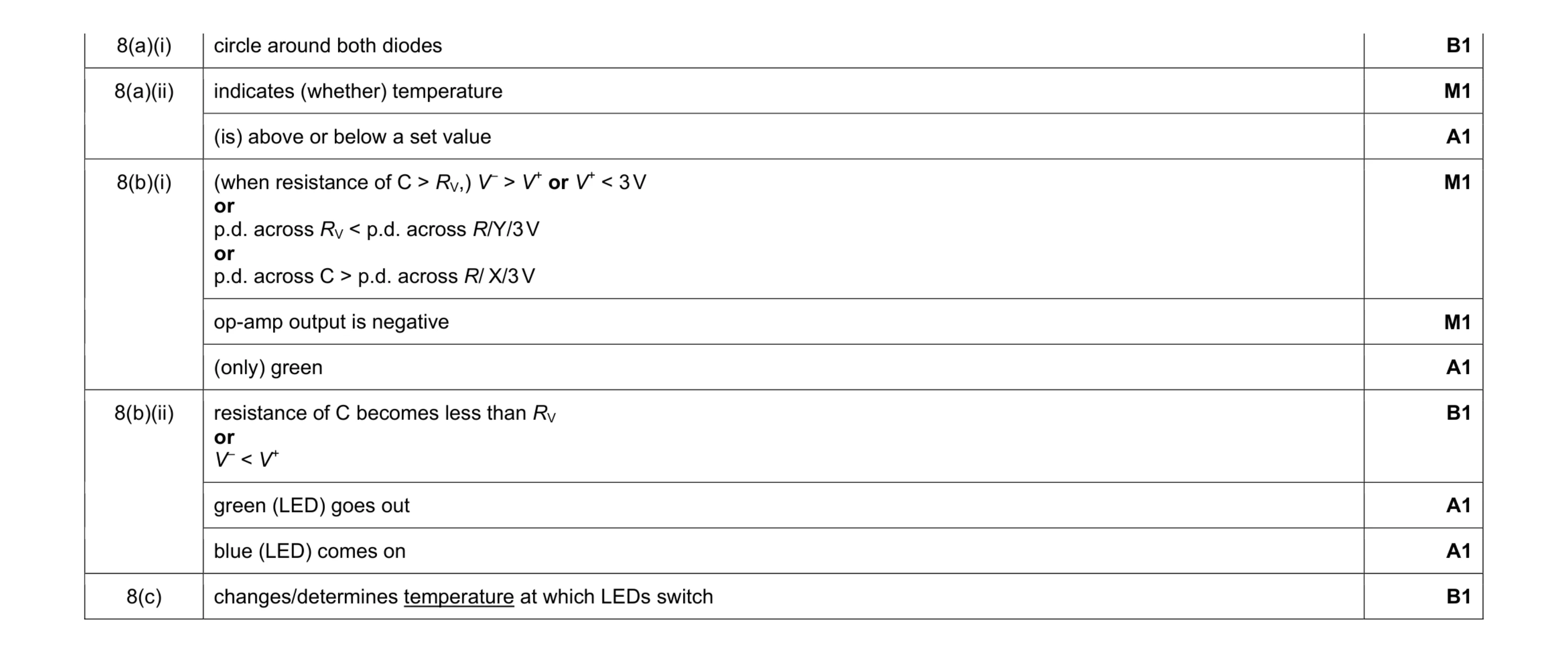 10
10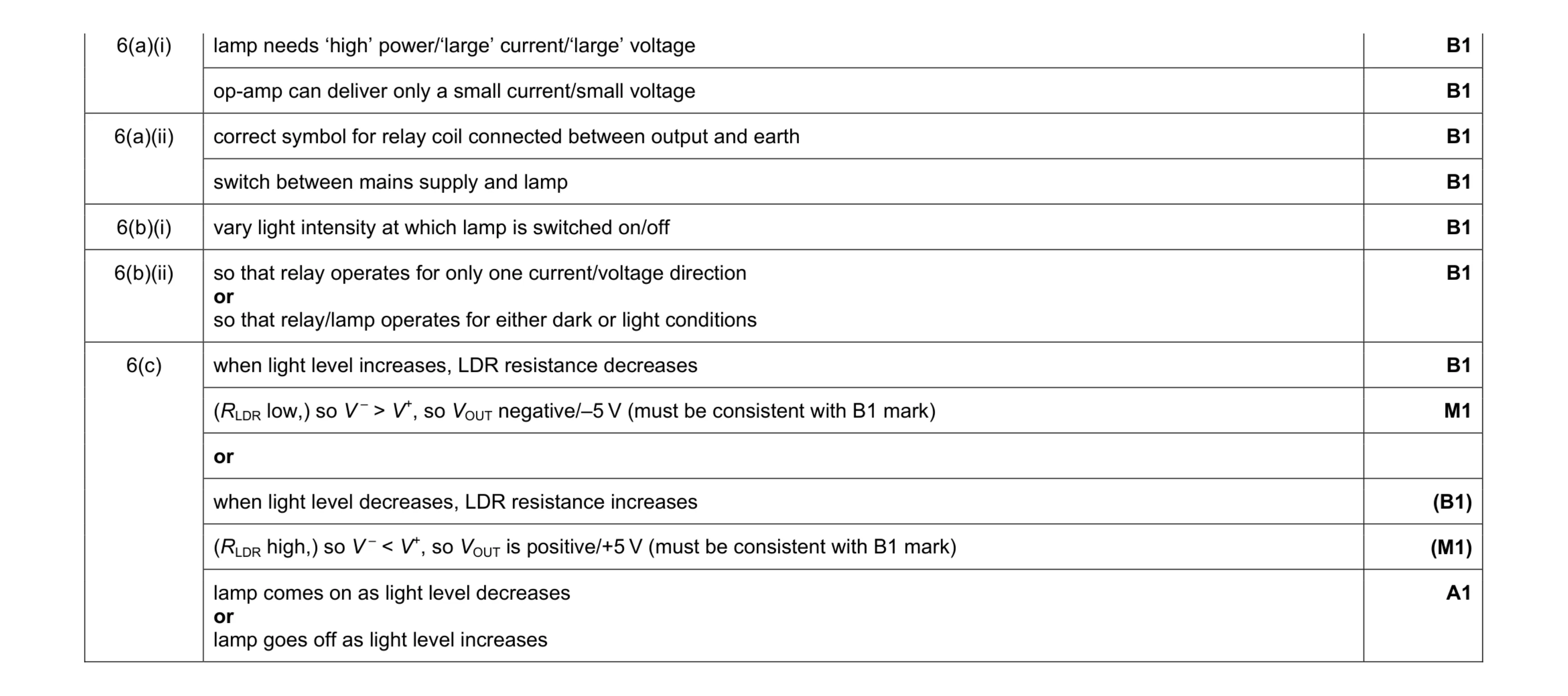 9
9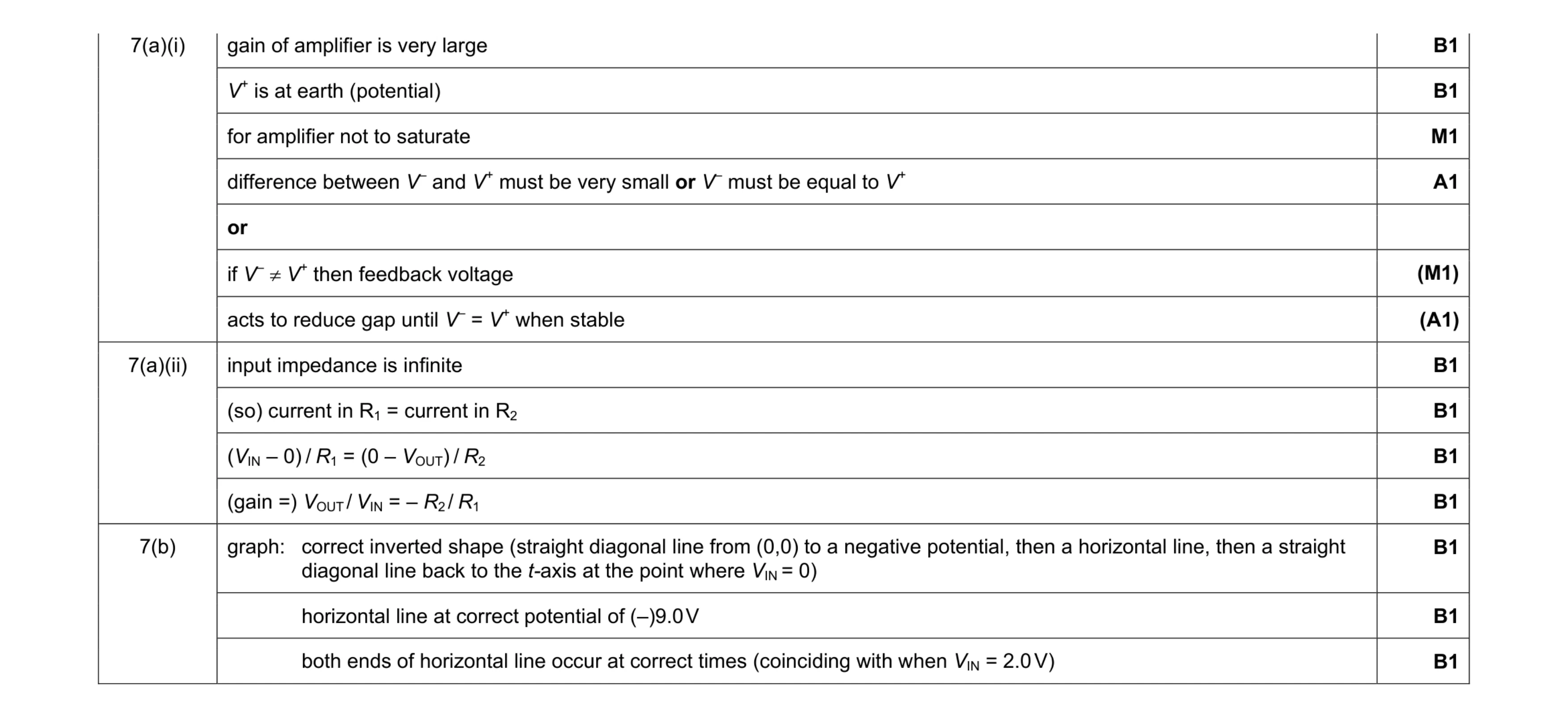 11
11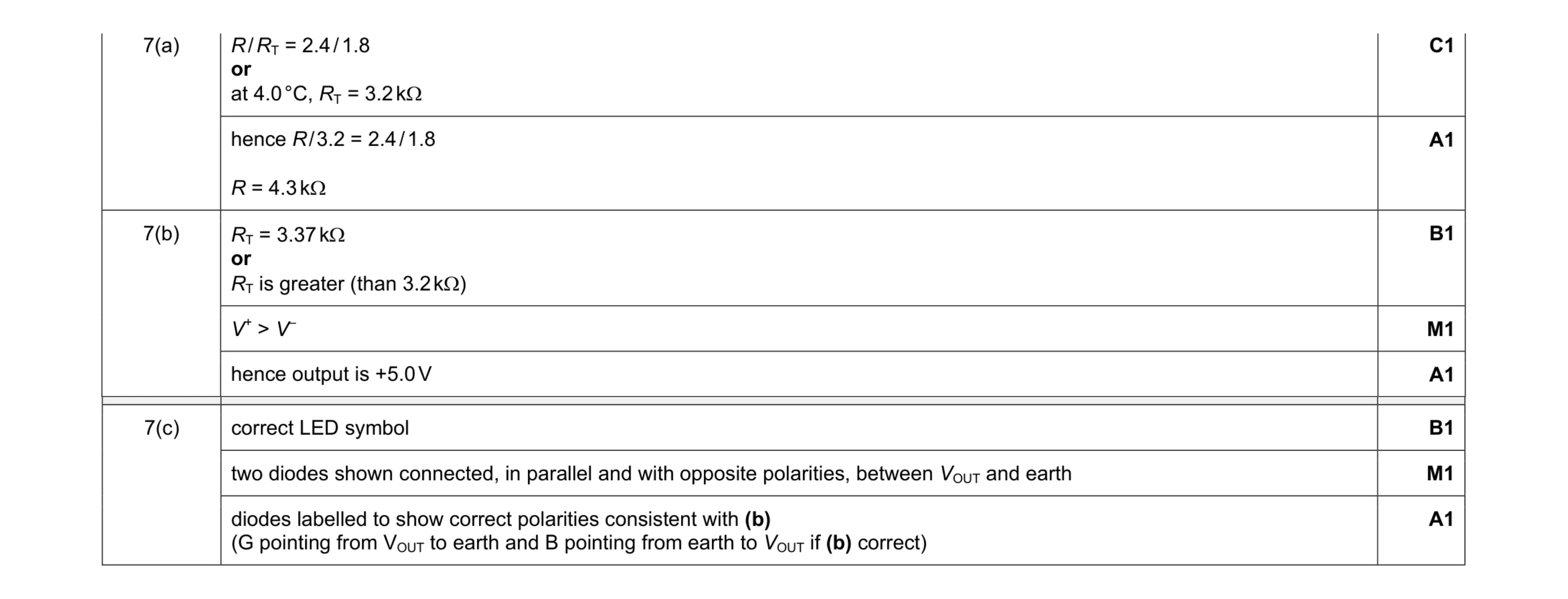 8
8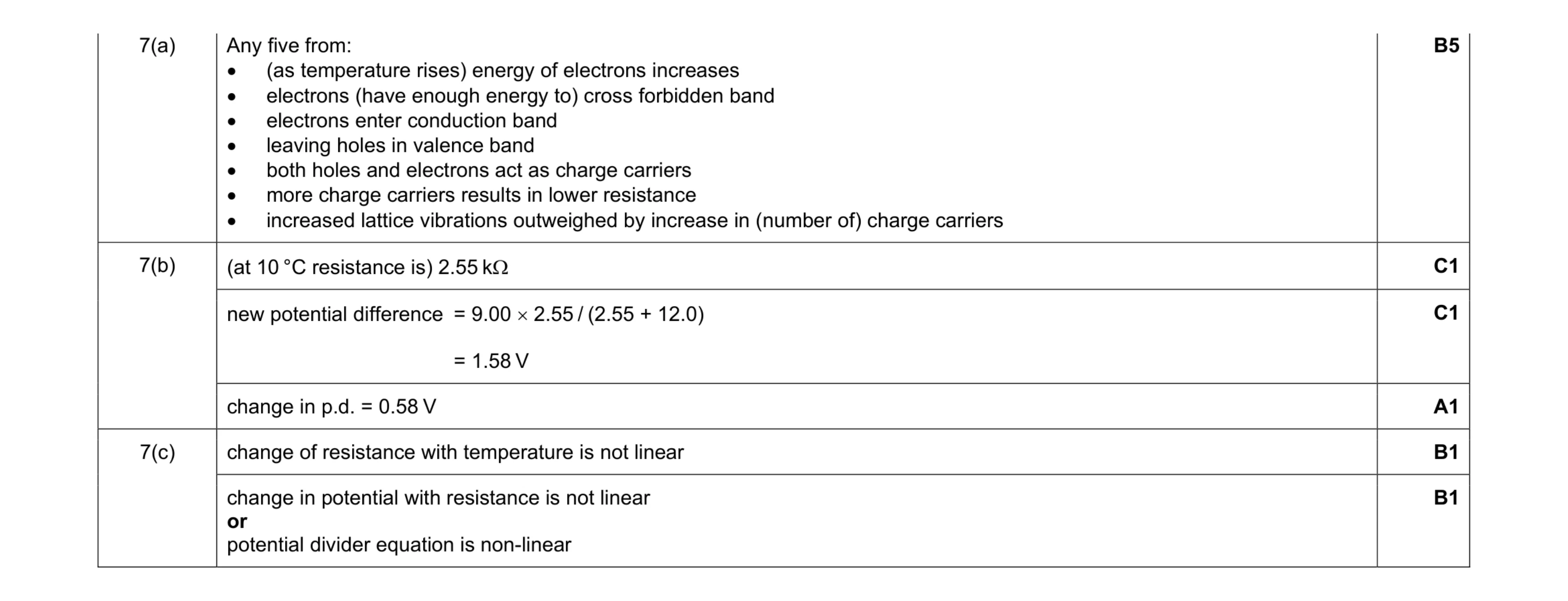 10
10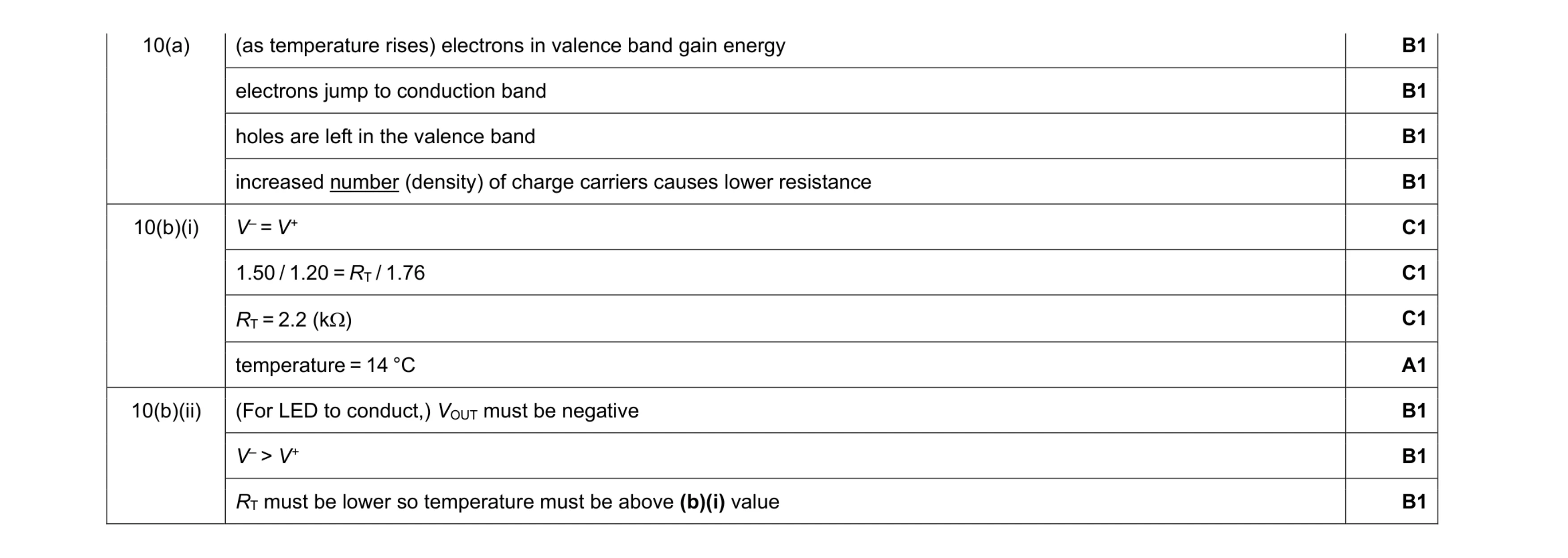 11
11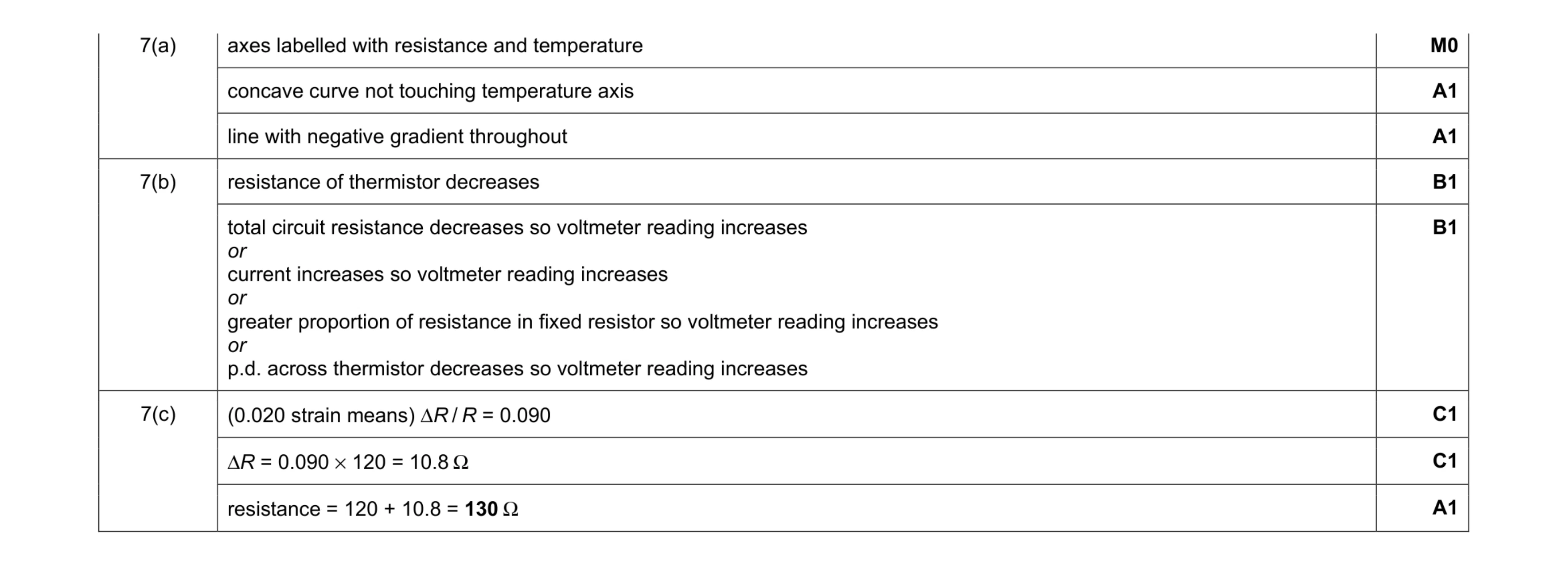 7
7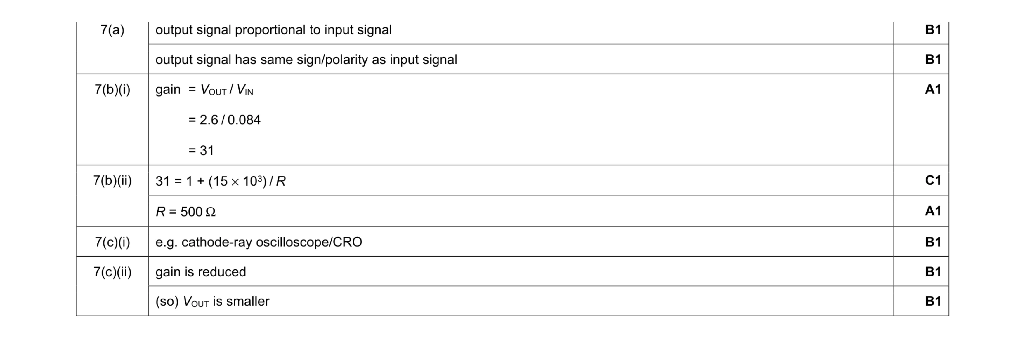 8
8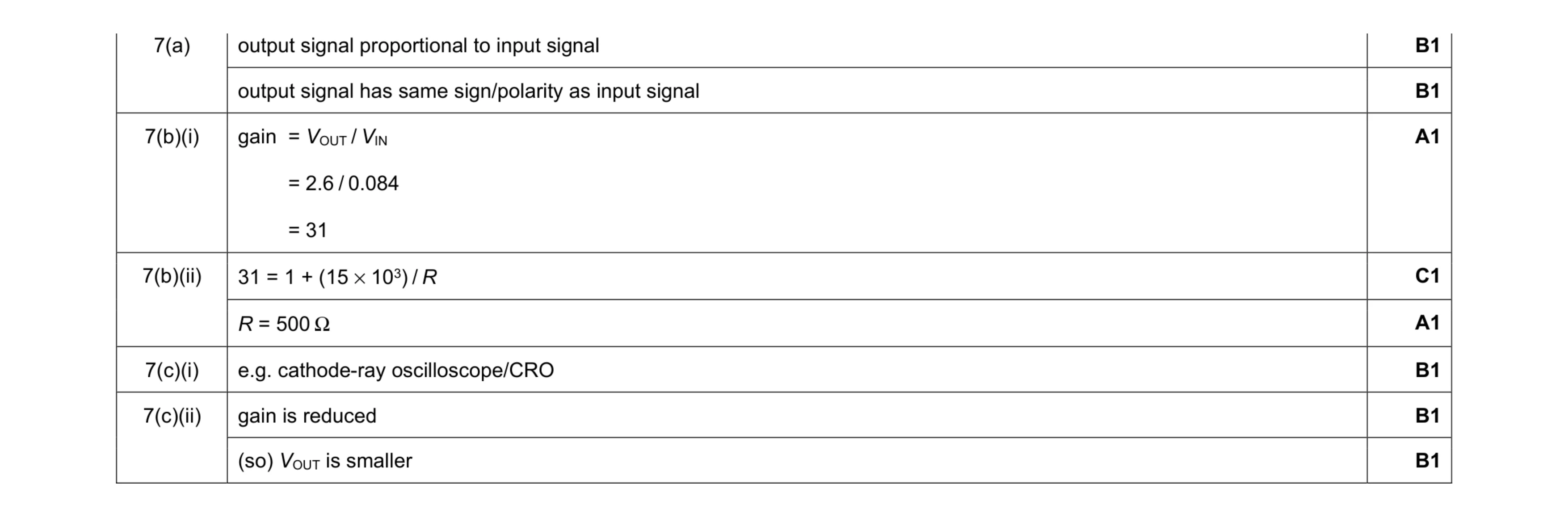 8
8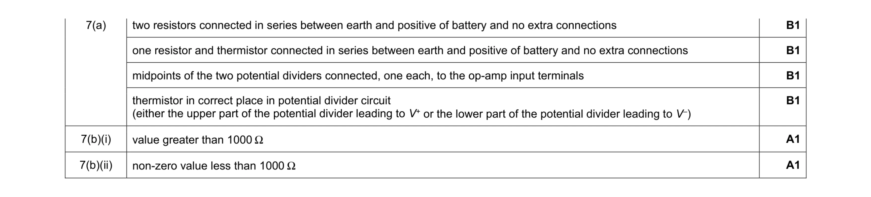 6
6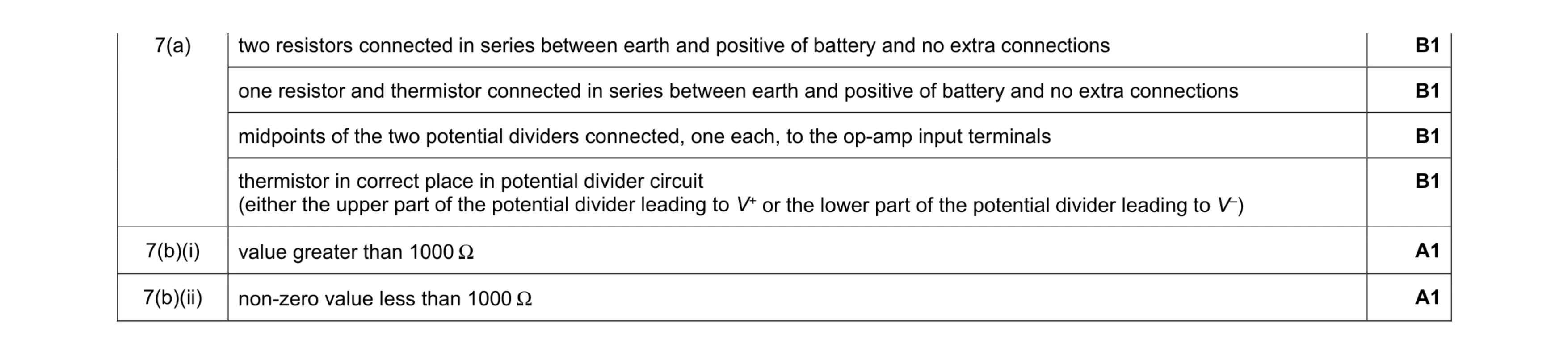 6
6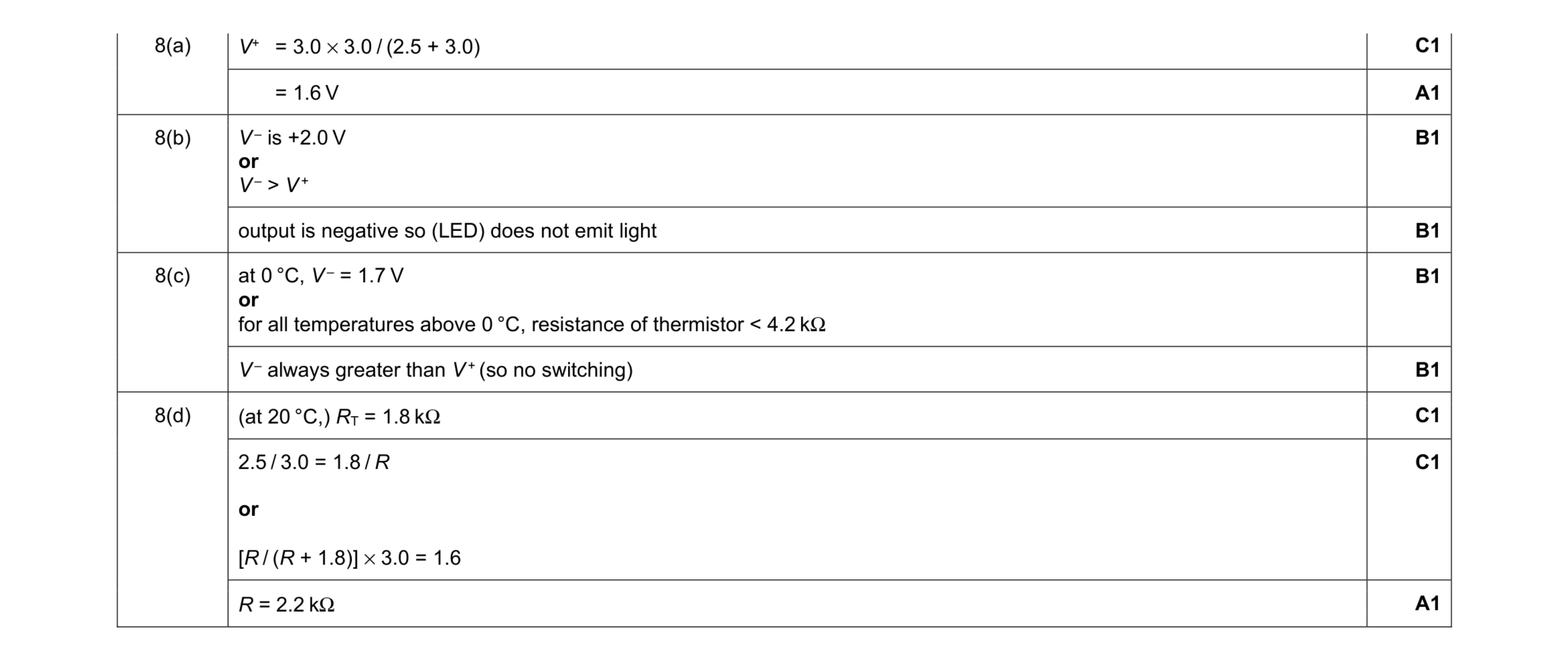 9
9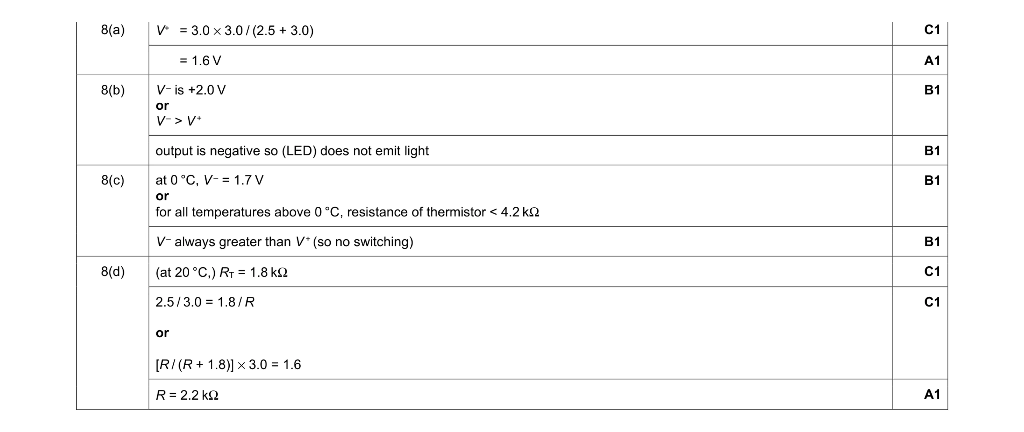 9
9