Questions as text
Q1 · The electrical resistance of a thermistor is to be used to measure temperatures in the… 9702/41 May/June 2006
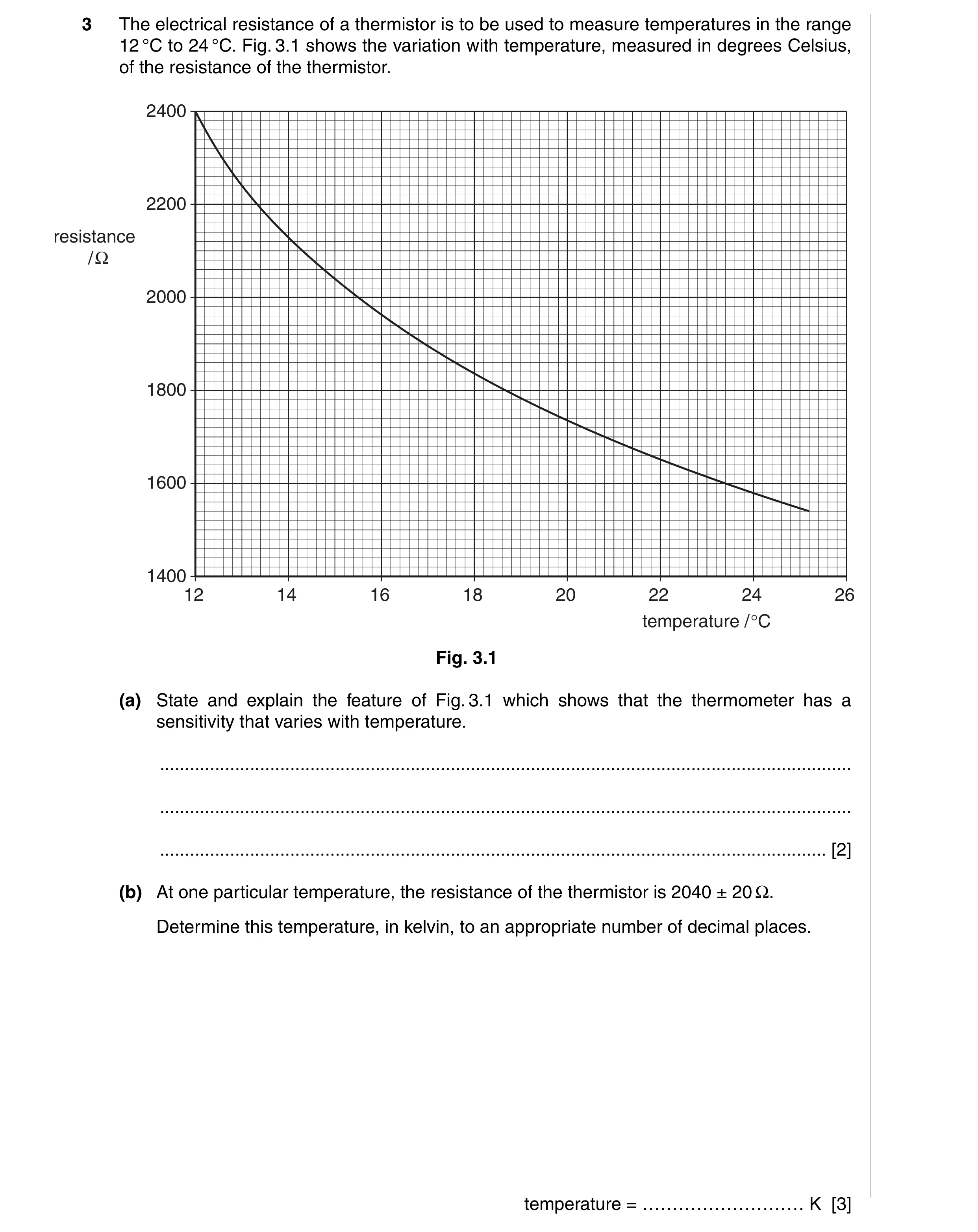
3 The electrical resistance of a thermistor is to be used to measure temperatures in the range 12 °C to 24 °C. Fig. 3.1 shows the variation with temperature, measured in degrees Celsius, of the resistance of the thermistor. 2400 2200 resistance / 2000 1800 1600 1400 12 14 16 18 20 22 24 26 temperature / Fig. 3.1 (a) State and explain the feature of Fig. 3.1 which shows that the thermometer has a sensitivity that varies with temperature. … … … [2] (b) At one particular temperature, the resistance of the thermistor is 2040 ± 20 Ω. Determine this temperature, in kelvin, to an appropriate number of decimal places. temperature = ……………………… K [3]
5 marks
Mark scheme: 3 (a) gradient of graph is (a measure of) the sensitivity M1 the gradient varies with temperature A1 [2] (b) 2040 ± 20 Ω corresponds to 15.0 ± 0.2 °C C1 T / K = T / °C + 273.15 (allow 273.2) C1 temperature is 288.2 K A1 [3]
This question in 9702/41 May/June 2006
Q2 · A student designs an electronic sensor to monitor whether the temperature in a… 9702/43 Oct/Nov 2012
9 A student designs an electronic sensor to monitor whether the temperature in a refrigerator is above or below a particular value. The circuit is shown in Fig. 9.1. A D +5 V – + –5 V B C sensing processing output device unit device Fig. 9.1 (a) Name the components used in the output device. … [1] (b) An operational amplifier (op-amp) is used as the processing unit. Describe the function of this processing unit. … … … [2] (c) State the function of (i) the resistors C and D, … … [1] (ii) the resistor B. … … [1] (d) The output device of the circuit in Fig. 9.1 is changed so that the new output device may For be used to switch on a high-voltage circuit. Examiner’s Use (i) State the component that is used in the new output device. … … [1] (ii) Draw on Fig. 9.2 to show how the component in (i), together with a diode, are connected so that the high voltage may be switched on when the output of the op-amp is negative. +5 V – + –5 V connections to high-voltage circuit output device Fig. 9.2 [2]
8 marks
Mark scheme: 9 (a) light-emitting diode (allow LED) B1 [1] (b) gives a high or a low output / +5 V or –5 V output M1 dependent on which of the inputs is at a higher potential A1 [2] (c) (i) provides a reference/constant potential B1 [1] (ii) determines temperature of ‘switch-over’ B1 [1] (d) (i) relay A1 [1] (ii) relay connected correctly for op-amp output and high-voltage circuit B1 diode with correct polarity in output from op-amp B1 [2]
This question in 9702/43 Oct/Nov 2012
Q3 · The volume of fuel in the fuel tank of a car is monitored using a sensing device 9702/42 May/June 2013
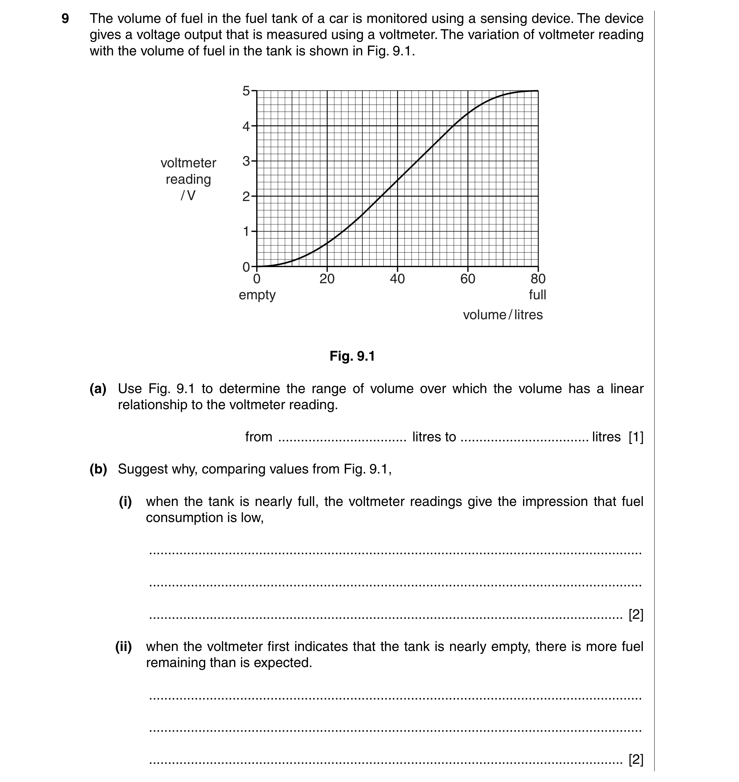
9 The volume of fuel in the fuel tank of a car is monitored using a sensing device. The device gives a voltage output that is measured using a voltmeter. The variation of voltmeter reading with the volume of fuel in the tank is shown in Fig. 9.1. 5 4 voltmeter 3 reading / V 2 1 0 0 20 40 60 80 empty full volume / litres Fig. 9.1 (a) Use Fig. 9.1 to determine the range of volume over which the volume has a linear relationship to the voltmeter reading. from … litres to … litres [1] (b) Suggest why, comparing values from Fig. 9.1, (i) when the tank is nearly full, the voltmeter readings give the impression that fuel consumption is low, … … … [2] (ii) when the voltmeter first indicates that the tank is nearly empty, there is more fuel remaining than is expected. … … … [2]
5 marks
Mark scheme: 9 (a) 30 litres → 54 litres (allow ± 4 litres on both limits) A1 [1] (b) (i) only 0.1 V change in reading for 10 litre consumption (or similar numbers) B1 above about 60 litres gradient is small compared to the gradient at about 40 litres B1 [2] (ii) voltmeter reading (nearly) zero when fuel is left C1 voltmeter reads only about 0.1 V when 10 litres of fuel left in tank A1 [2] (“voltmeter reads zero when about 4 litres of fuel left in tank” scores 2 marks)
This question in 9702/42 May/June 2013
Q4 · Suggest electrical sensing devices, one in each case, that may be used to monitor changes… 9702/43 May/June 2013
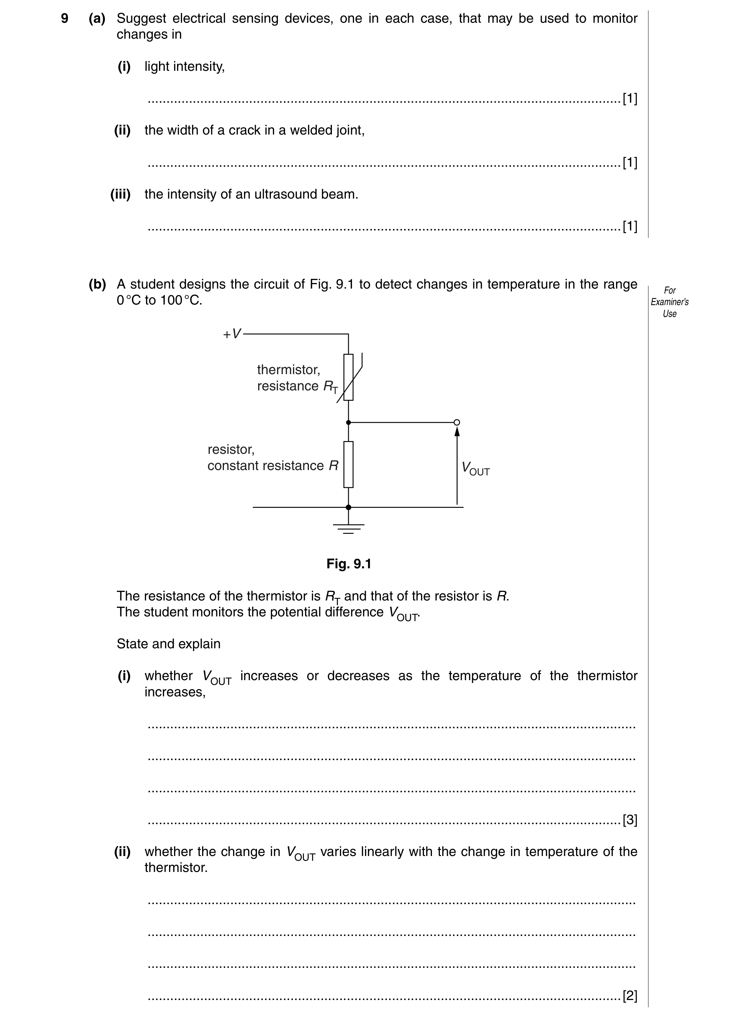
9 (a) Suggest electrical sensing devices, one in each case, that may be used to monitor changes in (i) light intensity, … [1] (ii) the width of a crack in a welded joint, … [1] (iii) the intensity of an ultrasound beam. … [1] (b) A student designs the circuit of Fig. 9.1 to detect changes in temperature in the range For 0 °C to 100 °C. Examiner’s Use +V thermistor, resistance RT resistor, constant resistance R VOUT Fig. 9.1 The resistance of the thermistor is RT and that of the resistor is R. The student monitors the potential difference VOUT. State and explain (i) whether VOUT increases or decreases as the temperature of the thermistor increases, … … … … [3] (ii) whether the change in VOUT varies linearly with the change in temperature of the thermistor. … … … … [2]
8 marks
Mark scheme: 9 (a) (i) light-dependent resistor/LDR B1 [1] (ii) strain gauge B1 [1] (iii) quartz/piezo-electric crystal B1 [1] (b) (i) resistance of thermistor decreases as temperature increses M1 etiher VOUT = V × R / (R + RT) or current increases and VOUT = I R A1 VOUT increases A1 [3] (ii) either change in RT with temperature is non-linear or VOUT is not proportional to RT/ change in VOUT with RT is non-linear M1 so change is non-linear A1 [2]
This question in 9702/43 May/June 2013
Q5 · An electronic sensor may be represented by the block diagram of Fig 9702/41 Oct/Nov 2013
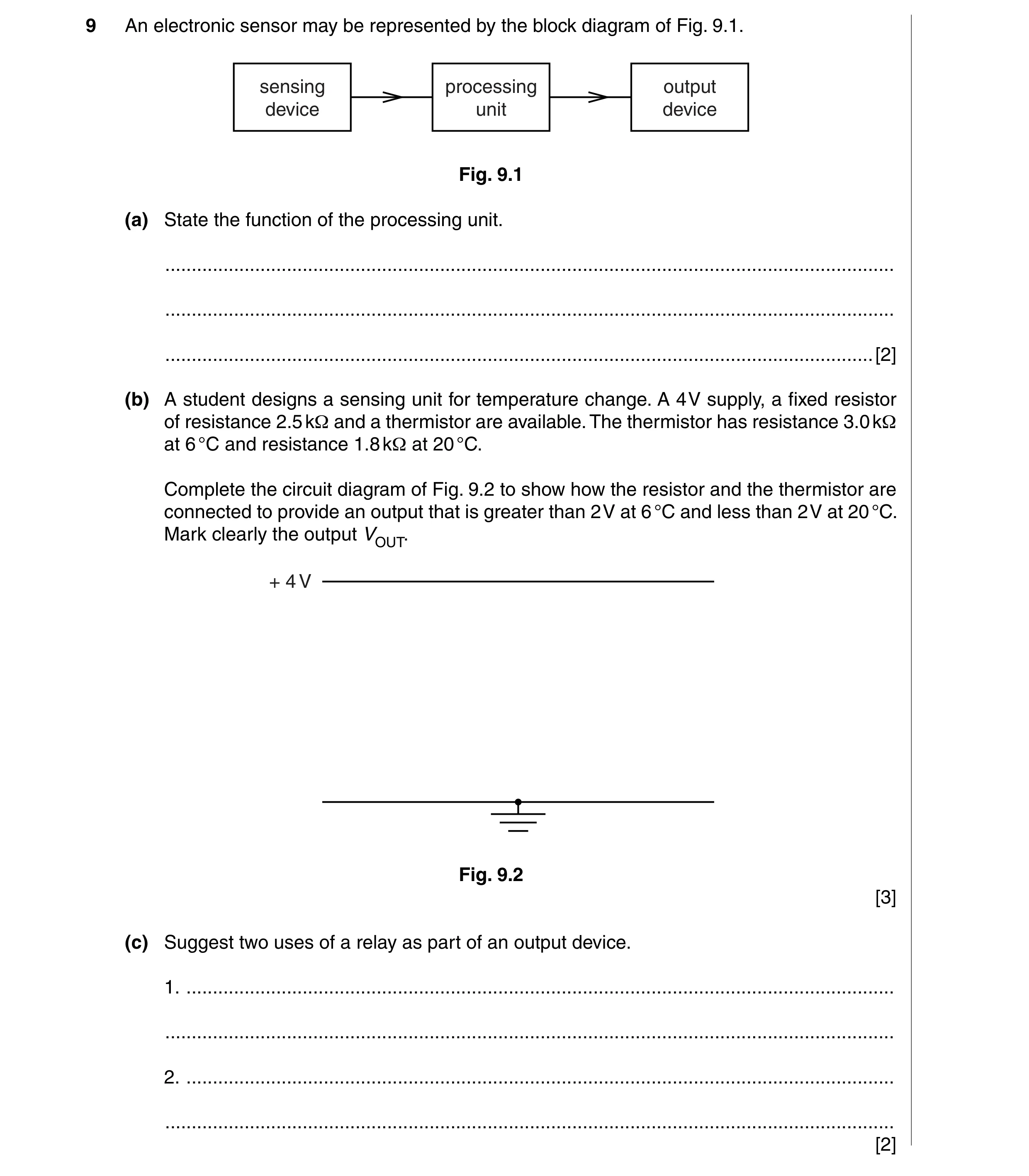
9 An electronic sensor may be represented by the block diagram of Fig. 9.1. sensing processing output device unit device Fig. 9.1 (a) State the function of the processing unit. … … … [2] (b) A student designs a sensing unit for temperature change. A 4 V supply, a fixed resistor of resistance 2.5 kΩ and a thermistor are available. The thermistor has resistance 3.0 kΩ at 6 °C and resistance 1.8 kΩ at 20 °C. Complete the circuit diagram of Fig. 9.2 to show how the resistor and the thermistor are connected to provide an output that is greater than 2 V at 6 °C and less than 2 V at 20 °C. Mark clearly the output VOUT. + 4 V Fig. 9.2 [3] (c) Suggest two uses of a relay as part of an output device. 1. … … 2. … … [2]
7 marks
Mark scheme: 9 (a) operates on / takes signal from sensing device B1 (so that) it gives an voltage output B1 [2] (b) thermistor and resistor in series between +4 V line and earth M1 VOUT shown clearly across either thermistor or resistor A1 VOUT shown clearly across thermistor A1 [3] (c) e.g. remote switching e.g. switching large current by means of a small current e.g. isolating circuit from high voltage e.g. switching high voltage by means of a small voltage/current (any two sensible suggestions, 1 each to max. 2) B2 [2]
This question in 9702/41 Oct/Nov 2013
Q6 · An electronic sensor may be represented by the block diagram of Fig 9702/42 Oct/Nov 2013
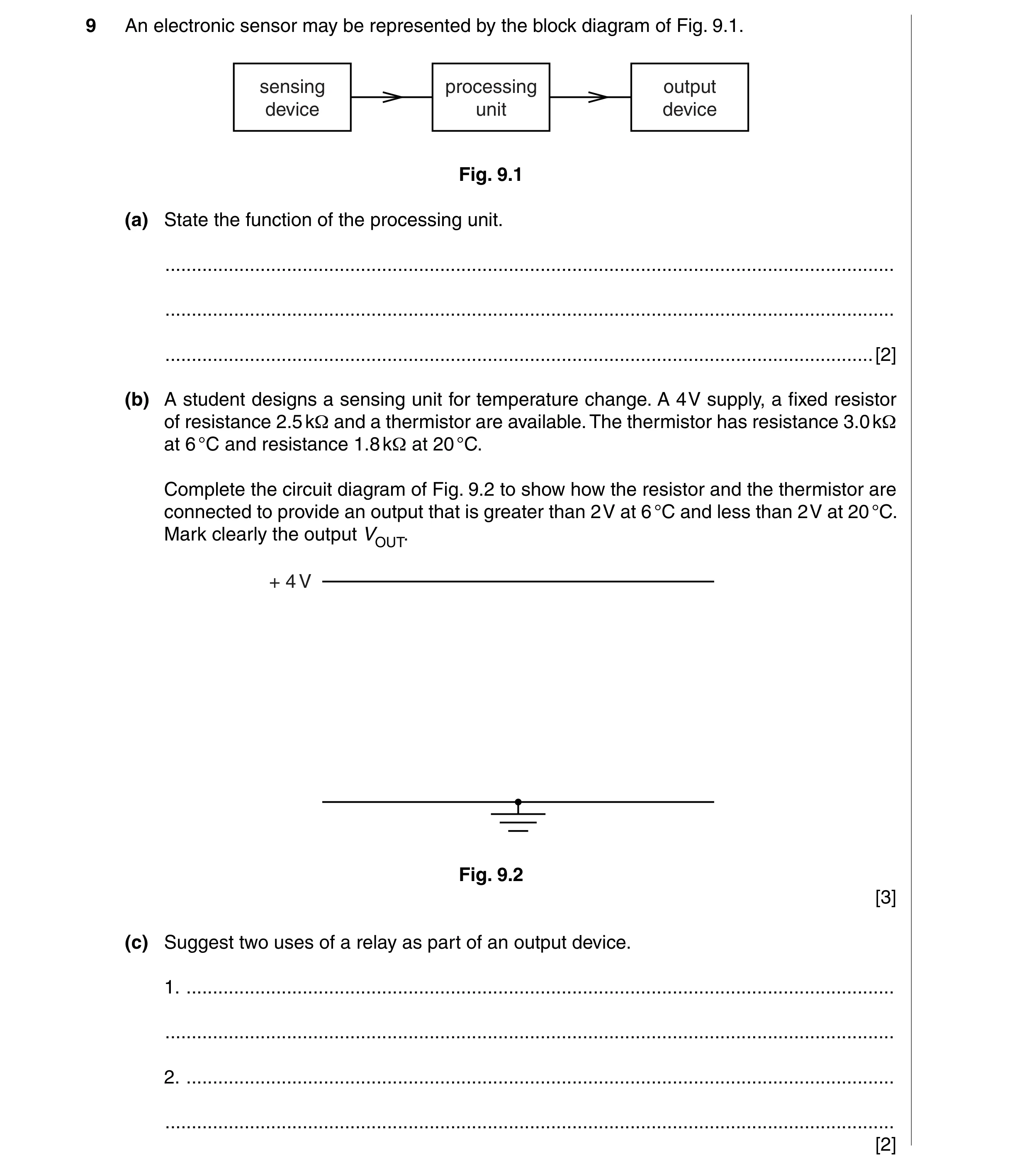
9 An electronic sensor may be represented by the block diagram of Fig. 9.1. sensing processing output device unit device Fig. 9.1 (a) State the function of the processing unit. … … … [2] (b) A student designs a sensing unit for temperature change. A 4 V supply, a fixed resistor of resistance 2.5 kΩ and a thermistor are available. The thermistor has resistance 3.0 kΩ at 6 °C and resistance 1.8 kΩ at 20 °C. Complete the circuit diagram of Fig. 9.2 to show how the resistor and the thermistor are connected to provide an output that is greater than 2 V at 6 °C and less than 2 V at 20 °C. Mark clearly the output VOUT. + 4 V Fig. 9.2 [3] (c) Suggest two uses of a relay as part of an output device. 1. … … 2. … … [2]
7 marks
Mark scheme: 9 (a) operates on / takes signal from sensing device B1 (so that) it gives an voltage output B1 [2] (b) thermistor and resistor in series between +4 V line and earth M1 VOUT shown clearly across either thermistor or resistor A1 VOUT shown clearly across thermistor A1 [3] (c) e.g. remote switching e.g. switching large current by means of a small current e.g. isolating circuit from high voltage e.g. switching high voltage by means of a small voltage/current (any two sensible suggestions, 1 each to max. 2) B2 [2]
This question in 9702/42 Oct/Nov 2013
Q7 · The mean value of an alternating current is zero 9702/42 Oct/Nov 2014
7 (a) The mean value of an alternating current is zero. Explain (i) why an alternating current gives rise to a heating effect in a resistor, … … … [2] (ii) by reference to heating effect, what is meant by the root-mean-square (r.m.s.) value of an alternating current. … … … … [2] (b) A simple iron-cored transformer is illustrated in Fig. 7.1. primary secondary coil coil iron core Fig. 7.1 (i) State Faraday’s law of electromagnetic induction. … … … [2] (ii) Use Faraday’s law to explain why the current in the primary coil is not in phase with the e.m.f. induced in the secondary coil. … … … … … [3]
9 marks
Mark scheme: 7 (a) (i) either heating effect in a resistor ∝ (current)2 B1 square of value of an alternating current is always positive B1 so heating effect A0 or current moves in opposite directions in resistor during half-cycles (B1) heating effect is independent of direction (B1) [2] (ii) that value of the direct current M1 producing the same heating effect (as the alternating current) in a resistor A1 [2] (b) (i) induced e.m.f. proportional to the rate M1 of change of (magnetic) flux (linkage) A1 [2] (ii) flux in core is in phase with current in the primary coil B1 (induced) e.m.f. in secondary because coil cuts the flux B1 flux and rate of change of flux are not in phase B1 [3]
This question in 9702/42 Oct/Nov 2014
Q8 · In many distribution systems for electrical energy, the energy is transmitted using… 9702/43 May/June 2015
7 In many distribution systems for electrical energy, the energy is transmitted using alternating current at high voltages. Suggest and explain an advantage, one in each case, for the use of (a) alternating voltages, … … … … [2] (b) high voltages. … … … … [2]
4 marks
Mark scheme: 7 (a) can change (output) voltage efficiently or to suit different consumers/appliances B1 by using transformers B1 [2] (b) for same power, current is smaller B1 less heating in cables/wires or thinner cables possible or less voltage loss in cables B1 [2]
This question in 9702/43 May/June 2015
Q9 · The variation with time t of the voltage level of part of an analogue signal is shown in… 9702/41 May/June 2016
5 The variation with time t of the voltage level of part of an analogue signal is shown in Fig. 5.1. 16 14 voltage level 12 10 8 6 4 2 0 0 0.25 0.50 0.75 1.00 1.25 1.50 time t / ms Fig. 5.1 The signal is sampled at 0.25 ms intervals. Each sample is converted into a four-bit digital number. Fig. 5.2 lists various times t at which the voltage level is sampled. The digital number for time t = 0 is shown. time t / ms 0 0.25 0.50 0.75 1.00 1.25 1.50 digital number 1011 Fig. 5.2 (a) (i) On Fig. 5.2, underline the most significant bit (MSB) for the digital number at time t = 0. [1] (ii) Complete Fig. 5.2 for the times shown. [2] (b) After transmission of the digital numbers, the signal is passed through a digital-to-analogue converter (DAC). On Fig. 5.3, plot the transmitted analogue signal from the DAC. 16 14 voltage level 12 10 8 6 4 2 0 0 0.25 0.50 0.75 1.00 1.25 1.50 time t / ms Fig. 5.3 [3] (c) The transmitted signal in (b) has less detail than the original signal in Fig. 5.1. Suggest and explain two means by which the level of detail in the transmitted signal could be increased. 1. … … … 2. … … … [4] [Total: 10]
10 marks
Mark scheme: 5 (a) (i) 1011 A1 [1] (ii) 0 0.25 0.50 0.75 1.00 1.25 1.50 1011 0110 1000 1110 0101 0011 0001 All 6 correct, 2 marks. 5 correct, 1 mark. A2 [2] (b) sketch: 6 horizontal steps of width 0.25 ms shown M1 steps at correct heights and all steps shown A1 steps shown in correct time intervals A1 [3] (c) increase sampling frequency/rate M1 so that step width/depth is reduced A1 increase number of bits (in each number) M1 so that step height is reduced A1 [4]
This question in 9702/41 May/June 2016
Q10 · The digital transmission of speech may be represented using the block diagram of Fig 9702/42 Feb/March 2018
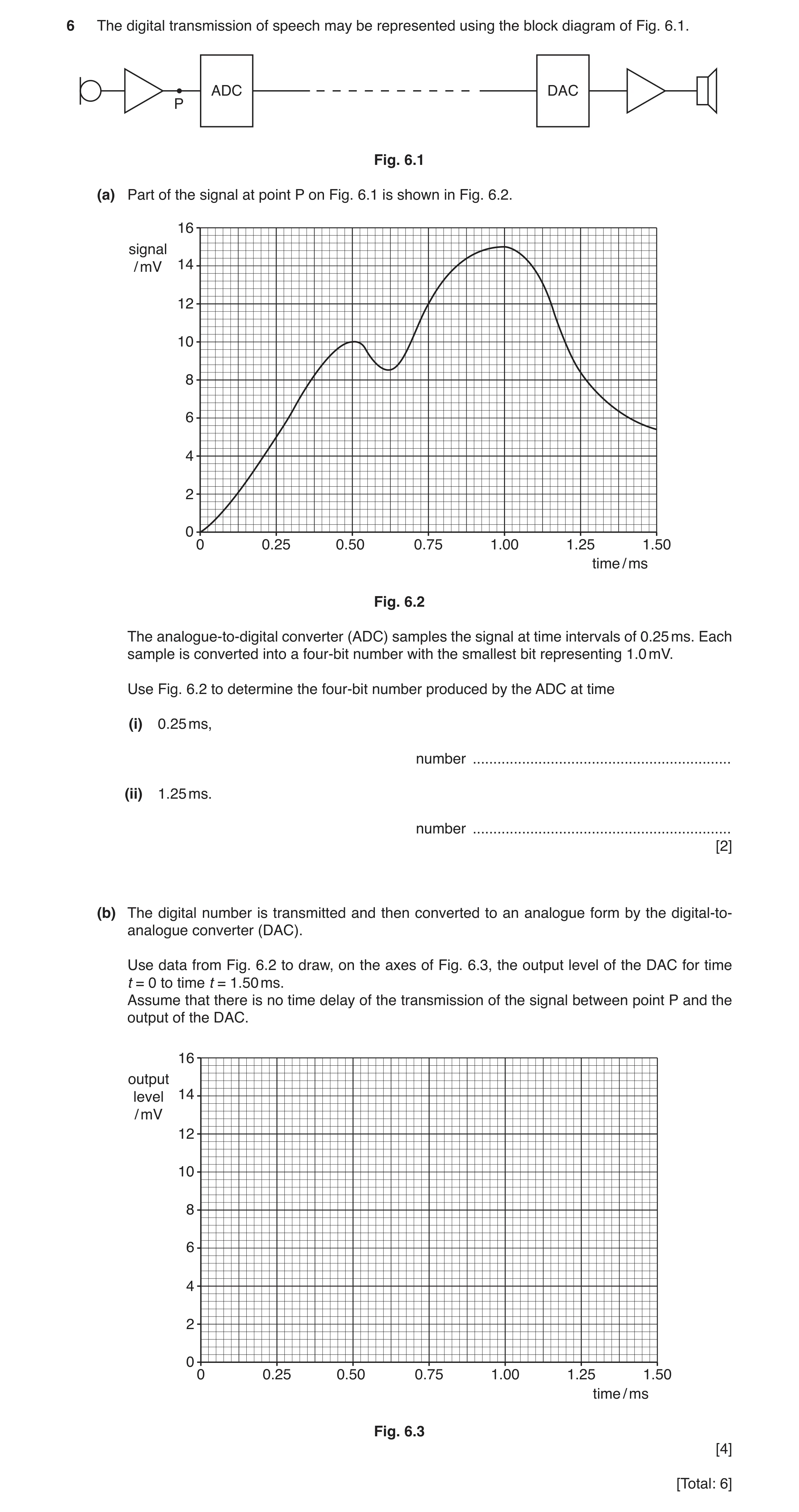
6 The digital transmission of speech may be represented using the block diagram of Fig. 6.1. ADC DAC P Fig. 6.1 (a) Part of the signal at point P on Fig. 6.1 is shown in Fig. 6.2. 16 signal / mV 14 12 10 8 6 4 2 0 0 0.25 0.50 0.75 1.00 1.25 1.50 time / ms Fig. 6.2 The analogue-to-digital converter (ADC) samples the signal at time intervals of 0.25 ms. Each sample is converted into a four-bit number with the smallest bit representing 1.0 mV. Use Fig. 6.2 to determine the four-bit number produced by the ADC at time (i) 0.25 ms, number … (ii) 1.25 ms. number … [2] (b) The digital number is transmitted and then converted to an analogue form by the digital-to- analogue converter (DAC). Use data from Fig. 6.2 to draw, on the axes of Fig. 6.3, the output level of the DAC for time t = 0 to time t = 1.50 ms. Assume that there is no time delay of the transmission of the signal between point P and the output of the DAC. 16 output level 14 / mV 12 10 8 6 4 2 0 0 0.25 0.50 0.75 1.00 1.25 1.50 time / ms Fig. 6.3 [4] [Total: 6]
6 marks
Mark scheme: 6(a)(i) 0101 A1 6(a)(ii) 1000 A1 6(b) sketch: series of steps B1 changes every 0.25 ms B1 correct heights 0, 5, 10, 12, 15, 8 at correct times Two marks for all levels correct One mark if one mistake B2
This question in 9702/42 Feb/March 2018
 1 / 13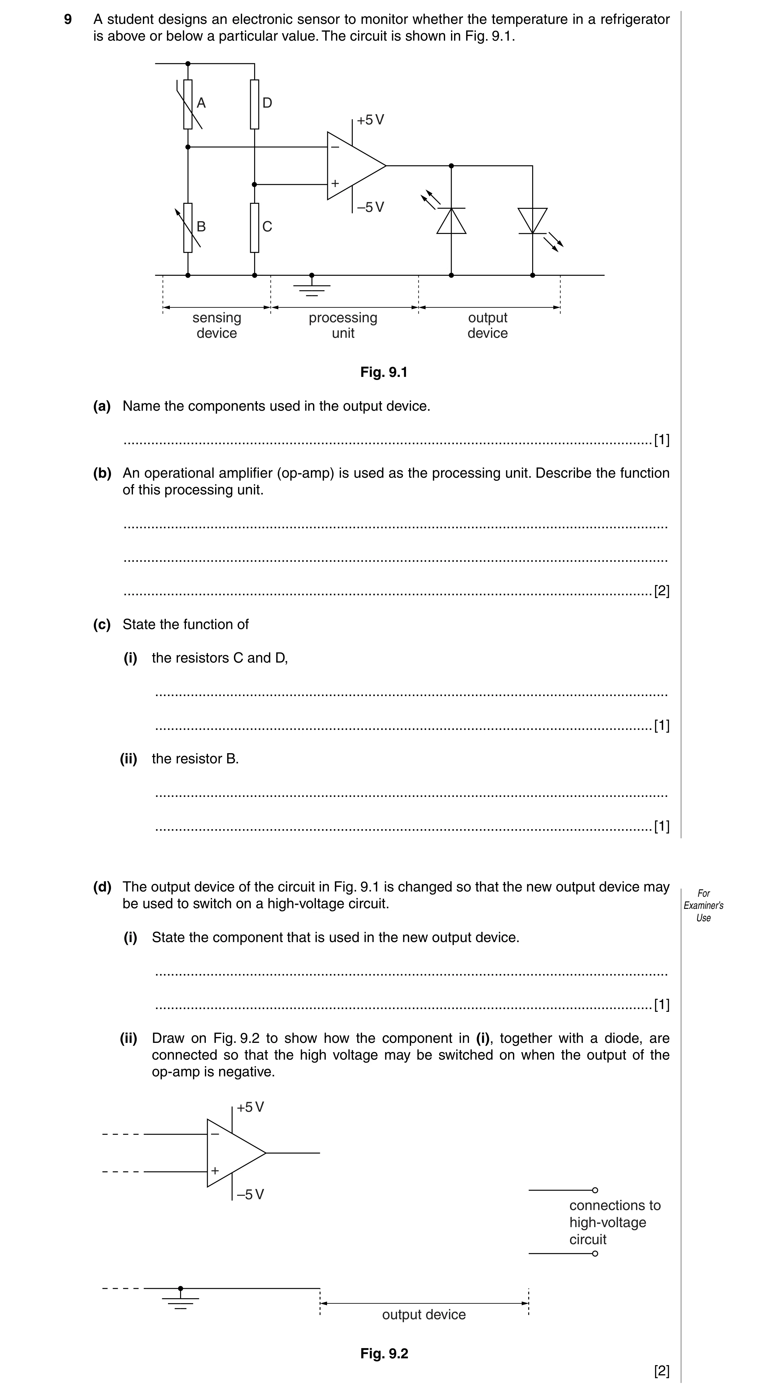
 4 / 13
 5 / 13
 6 / 13
 7 / 13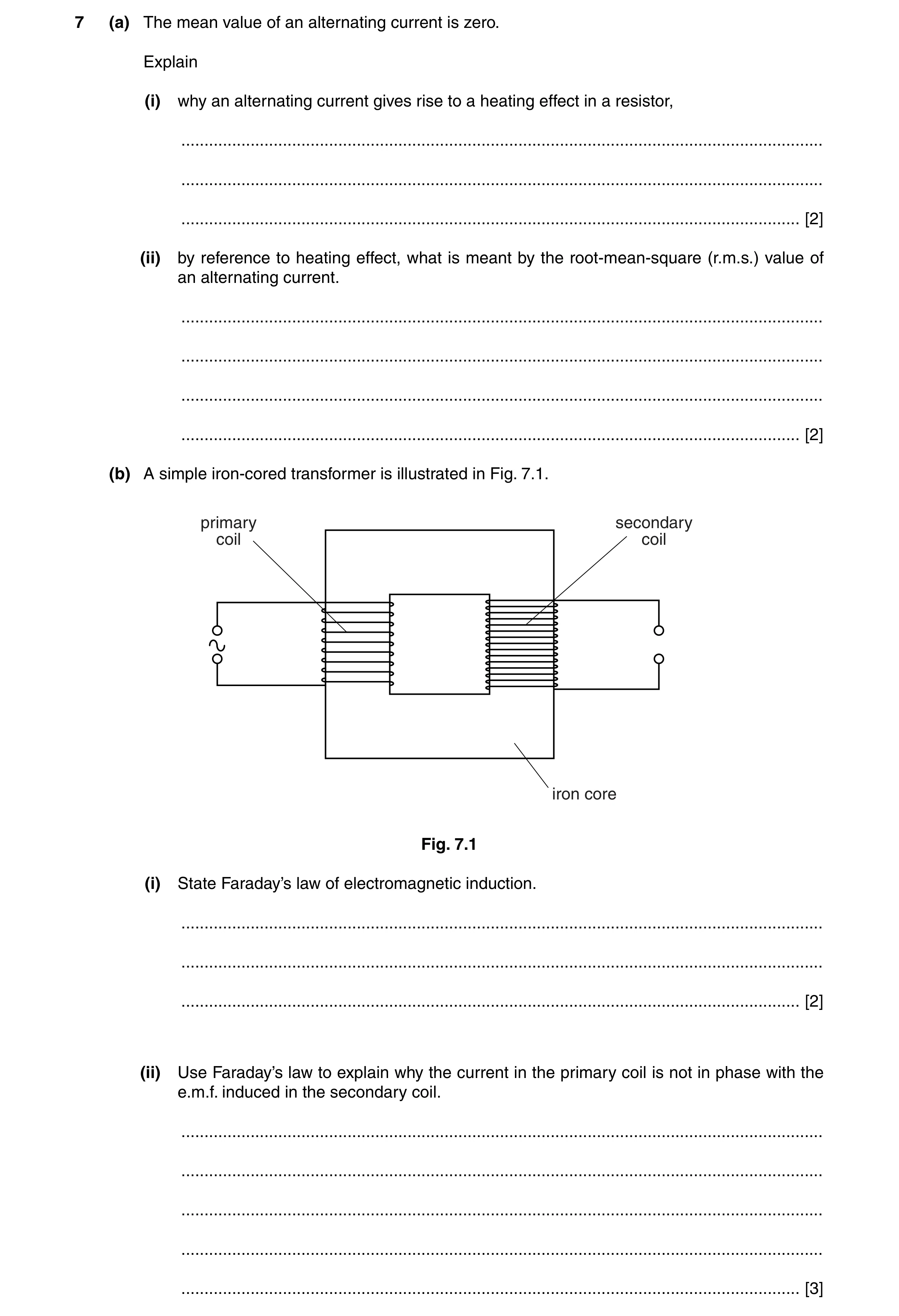
 9 / 13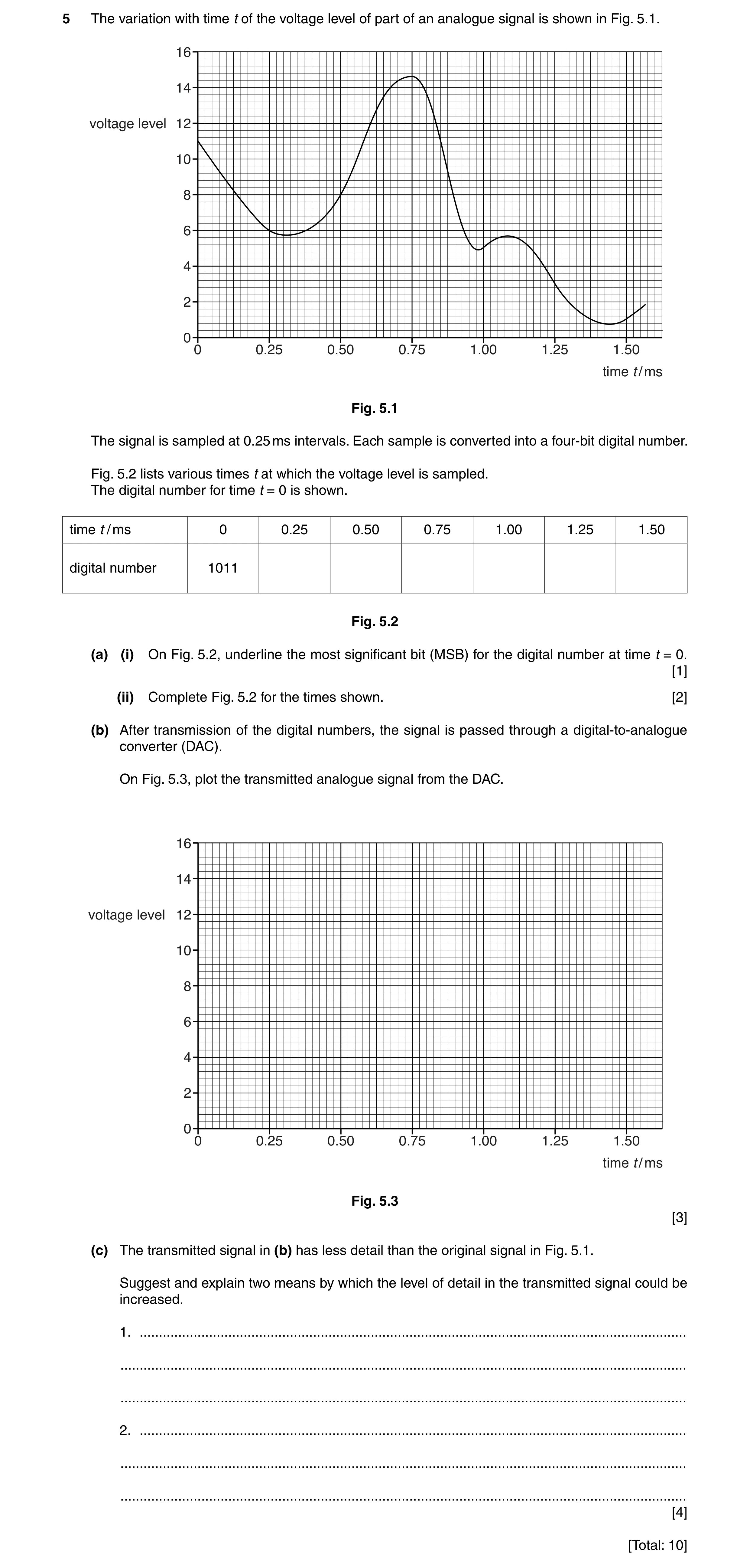
 5
5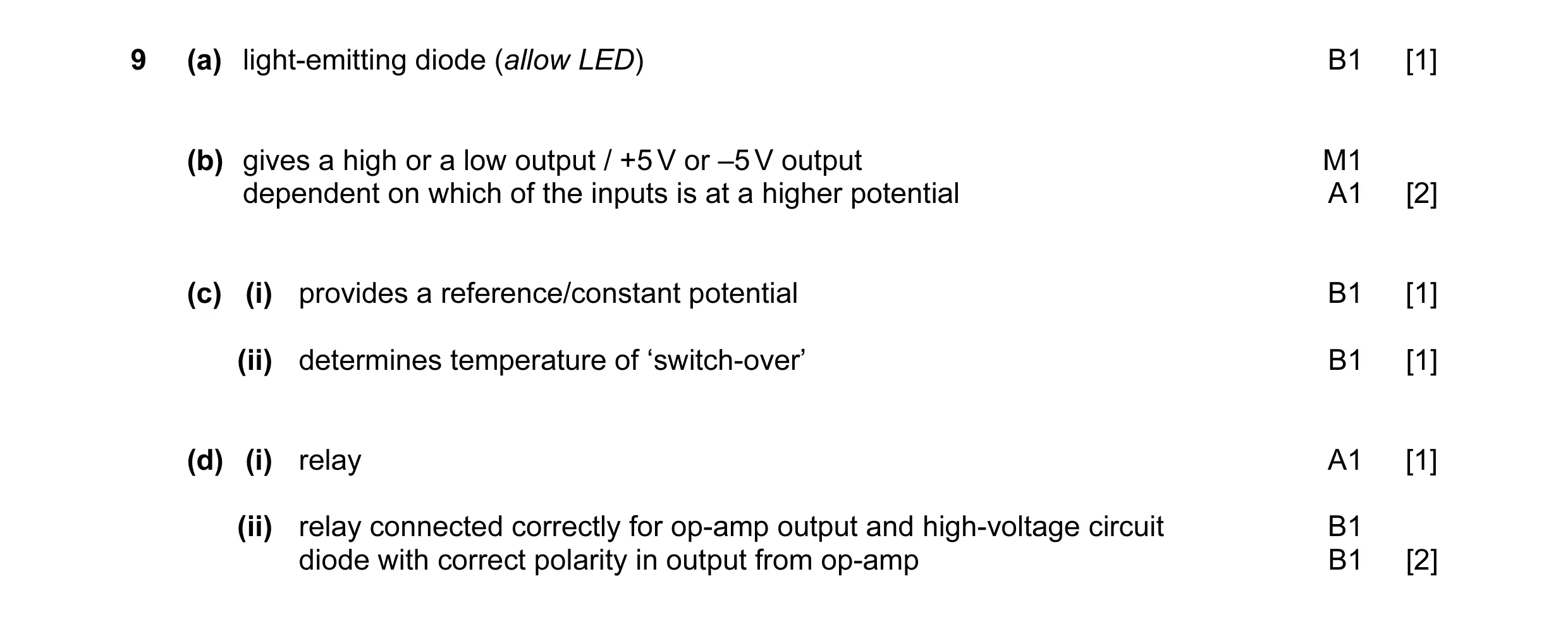 8
8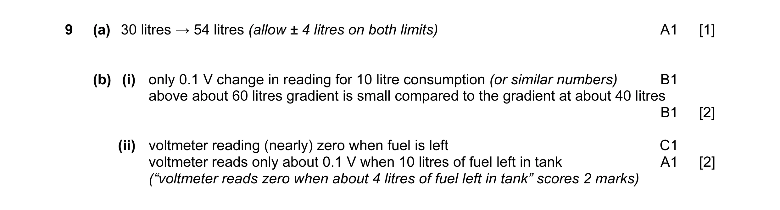 5
5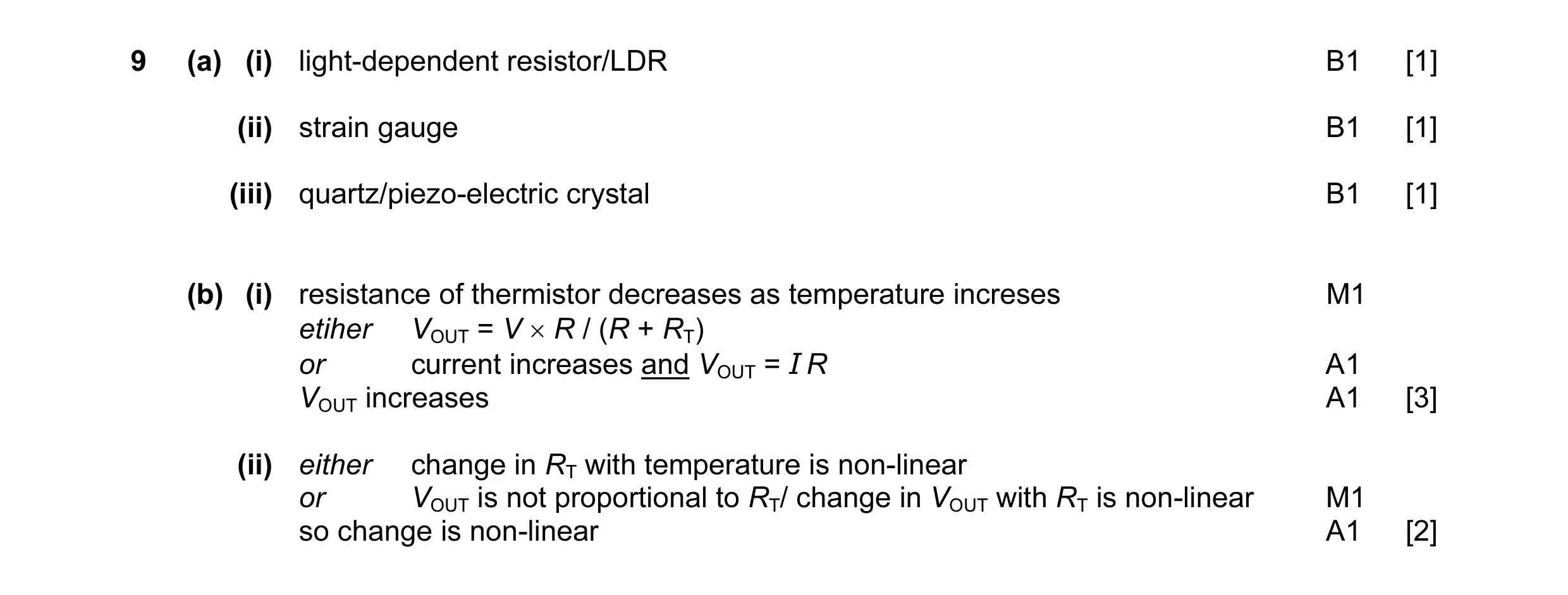 8
8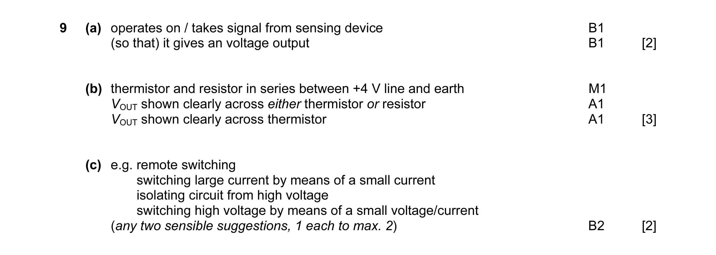 7
7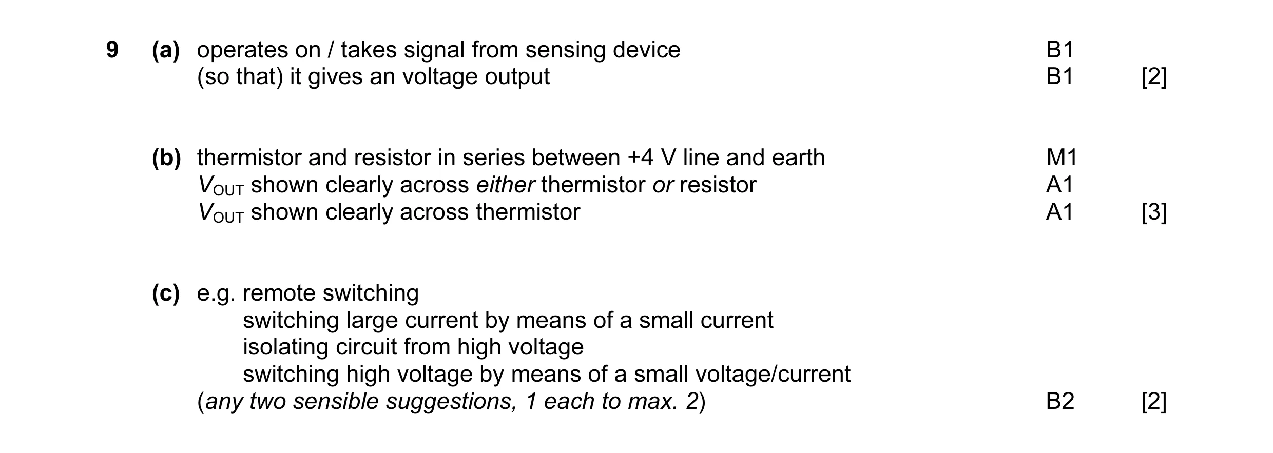 7
7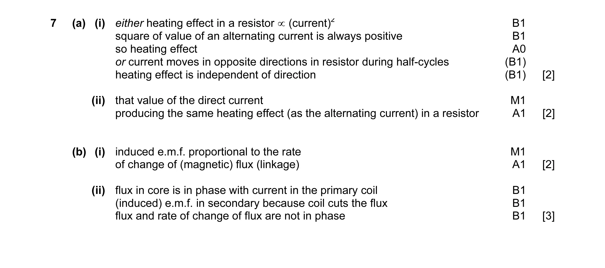 9
9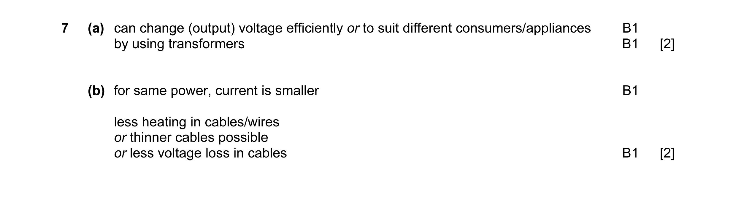 4
4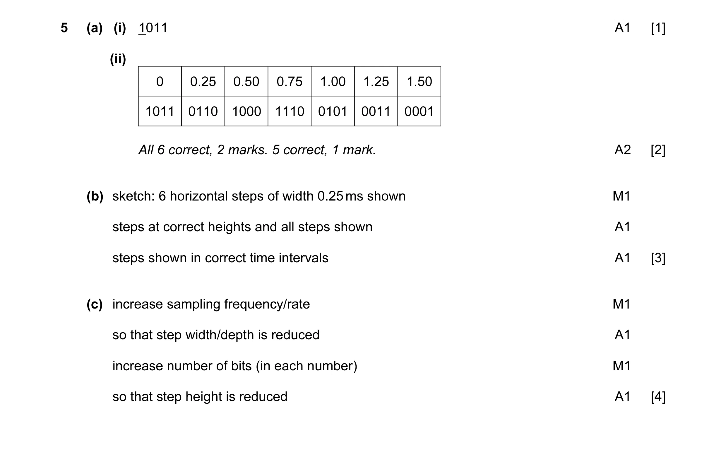 10
10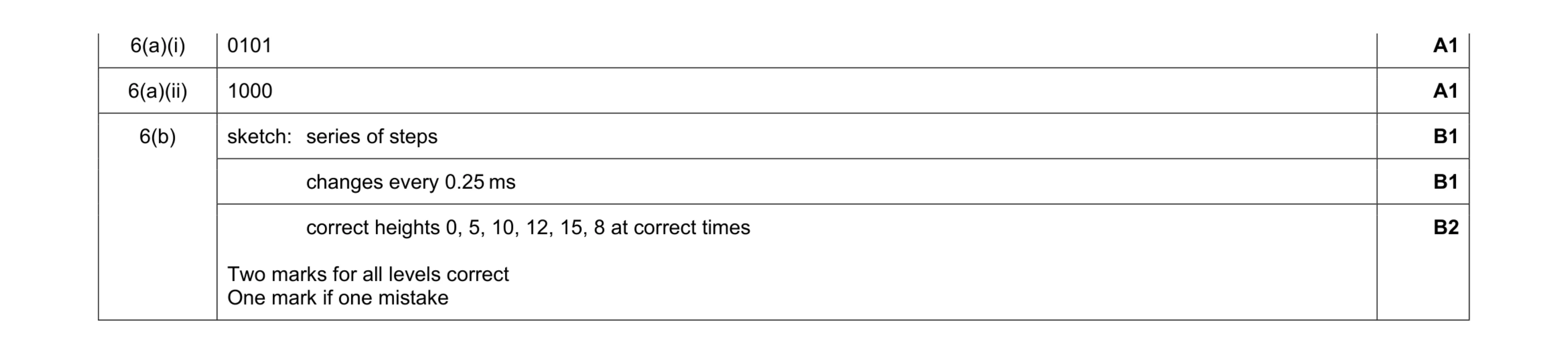 6
6